EP1362286B1 - Datenverarbeitung mittels eines zusatzprozessors - Google Patents
Datenverarbeitung mittels eines zusatzprozessors Download PDFInfo
- Publication number
- EP1362286B1 EP1362286B1 EP01273773.0A EP01273773A EP1362286B1 EP 1362286 B1 EP1362286 B1 EP 1362286B1 EP 01273773 A EP01273773 A EP 01273773A EP 1362286 B1 EP1362286 B1 EP 1362286B1
- Authority
- EP
- European Patent Office
- Prior art keywords
- coprocessor
- data
- main processor
- data words
- register
- Prior art date
- Legal status (The legal status is an assumption and is not a legal conclusion. Google has not performed a legal analysis and makes no representation as to the accuracy of the status listed.)
- Expired - Lifetime
Links
Images


Classifications
-
- G—PHYSICS
- G06—COMPUTING OR CALCULATING; COUNTING
- G06F—ELECTRIC DIGITAL DATA PROCESSING
- G06F13/00—Interconnection of, or transfer of information or other signals between, memories, input/output devices or central processing units
- G06F13/14—Handling requests for interconnection or transfer
-
- G—PHYSICS
- G06—COMPUTING OR CALCULATING; COUNTING
- G06F—ELECTRIC DIGITAL DATA PROCESSING
- G06F13/00—Interconnection of, or transfer of information or other signals between, memories, input/output devices or central processing units
- G06F13/38—Information transfer, e.g. on bus
- G06F13/42—Bus transfer protocol, e.g. handshake; Synchronisation
- G06F13/4204—Bus transfer protocol, e.g. handshake; Synchronisation on a parallel bus
- G06F13/4208—Bus transfer protocol, e.g. handshake; Synchronisation on a parallel bus being a system bus, e.g. VME bus, Futurebus, Multibus
- G06F13/4217—Bus transfer protocol, e.g. handshake; Synchronisation on a parallel bus being a system bus, e.g. VME bus, Futurebus, Multibus with synchronous protocol
Definitions
- This invention relates to data processing systems. More particularly, this invention relates to data processing systems incorporating both a main processor and a coprocessor.
- Coprocessors are often used to provide additional functionality within a data processing system that is not required in the basic system, but may be useful in certain circumstances when the additional overhead of providing a suitable coprocessor is justified.
- Particularly demanding data processing environment are those that involve digital signal processing, such as video image manipulation.
- the volumes of data that require processing in such applications can be high. This presents a challenge to provide data processing systems able to cope with the volume of processing necessary whilst simultaneously having a relatively low cost and low power consumption.
- Such special purpose circuitry can have an architecture specifically adapted to perform a relatively restricted range of processing operations, but at a relatively high speed.
- multiple data channels may be provided to stream data into and out of the relevant circuit portions in parallel. Whilst such an arrangement may be able to cope with the high data processing volumes required, it generally has the disadvantage of being inflexible. This inflexibility may mean that a relatively minor change in the algorithm it is desired to execute could require expensive corresponding hardware changes. This contrasts with a general purpose processor which is generally designed from the outset to be able to execute an enormous variety of different algorithms.
- EP 0 377 990 describes a data processing system which includes the means to access multi-word floating point data on either even or odd memory address boundaries.
- the present invention provides data processing apparatus comprising:
- the invention recognises that within a system containing a general purpose main processor, a coprocessor may be provided with very specific functions in mind.
- considerable advantages in terms of speed and code density may be achieved by providing that the coprocessor load instructions also trigger data processing operations to be performed upon operands within the loaded data words to generate result data words.
- a coprocessor has a highly specific role within the system, it has been found that in combination with a general purpose main processor, such a combination is able to provide an advantageous increase in the processing throughput whilst maintaining the ability of a general purpose processor to accommodate different algorithms and circumstances.
- Particularly preferred embodiments of the invention are ones in which a coprocessor memory is provided within the coprocessor to store locally data words to be used as operands in combination with the loaded data words.
- a coprocessor memory is provided within the coprocessor to store locally data words to be used as operands in combination with the loaded data words.
- the performance of the system is improved in embodiments in which loaded data words to be retrieved from a memory coupled to the main processor are passed to the coprocessor without being stored within registers of the main processor.
- the main processor can provide the role of an address generator and memory access mechanism for the coprocessor.
- main processor includes a register operable to store an address value pointing to the data words to be loaded into the coprocessor. This gives control of the address pointer to the main processor thereby yielding an improved degree of flexibility in the type of algorithm that may be supported.
- the data words to be loaded and manipulated could have a variety of widths.
- the data words could be 32-bit data words containing four 8-bit operands each representing an 8-bit pixel value.
- the data words and operands could take a wide variety of different sizes, such as 16-bits, 64-bits, 128-bits, or the like.
- preferred embodiments may use a register value within the coprocessor to store an alignment value specifying the alignment between the data operands and the data words and to which the coprocessor may be responsive to control how many data words are loaded for each coprocessor load instruction.
- the coprocessor could perform a wide variety of processing operations upon the operands within the loaded data words depending upon the particular system, the invention is particularly useful in systems where it is desired to perform of sum of absolute differences between a plurality of operand values.
- Performing a sum of absolute differences for a large quantity of data often represents a significant portion of the processing load required by a general purpose processor in carrying out operations such as pixel block matching during image processing.
- Offloading the bulk of the low level calculation of the sum of absolute differences to a coprocessor allows a significant increase in performance to be achieved whilst retaining the flexibility of the general purpose processor to employ the special purpose sum of absolute differences calculations as part of a wide variety of different algorithms.
- an accumulate register may advantageously be provided within the coprocessor to accumulate the total sum of absolute differences calculated. This accumulate register within the coprocessor can be retrieved back into the main processor for further manipulation as required but held locally within the coprocessor to speed operation and reduce the requirements for data transfer between the coprocessor and the main processor.
- the coprocessor load instructions may advantageously include an offset value to be applied to the address value stored as a pointer within the main processor.
- the offset value may optionally be used to update the pointer value either before or after the pointer value is used.
- the invention also provides a computer program product incorporating the coprocessor load instructions as described above.
- the computer programme product may be in the form of a distributable medium, such as a compact disk or a floppy disk, or may be part of firmware embedded within a device or may be dynamically downloaded, such as via a network link.
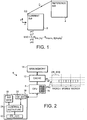
- Figure 1 shows a current block of pixels 2 for which it is desired to find the best match within a reference image.
- the current block of pixels comprises an 8*8 block of 8-bit pixel byte values.
- the current block of pixels 2 is compared with reference blocks of pixels 4 located at different vector displacements v from the current block of pixels 2.
- the sum of absolute differences expression illustrated in Figure 1 is calculated. This expression determines the absolute difference between respective corresponding pixel values for the two blocks and sums the 64 absolute difference values obtained.
- a good image match is generally indicated by a low sum of absolute differences value.
- an image data processing system such as one performing MPEG type processing, such a sum of absolute differences calculation is often required and can represent a disadvantageously large processing overhead for a general purpose processor.
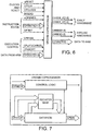
- Figure 2 illustrates a data processing system 6 including a main processor 8, a coprocessor 10, a cache memory 12 and a main memory 14.
- the main processor 8 includes a register bank 16 storing general purpose register values that may be utilised by the main processor 8.
- the main processor 8 may be, for example, one of the main processors designed by ARM Limited, Cambridge, England.
- the main processor 8 is coupled to the cache memory 12, which serves to provide high speed access to the most frequently required data values.
- a lower speed, but higher capacity, main memory 14 is provided outside of the cache 12.
- the coprocessor 10 is coupled to a coprocessor bus of the main processor 8 and is responsive to coprocessor instructions received and executed by the main processor 8 to carry out predefined operations.
- load coprocessor instructions that serve to load a data value into a coprocessor.
- the coprocessor 10 shown in Figure 2 extends the functionality of such coprocessor load instructions to also use them to specify to the coprocessor that it should carry out certain predefined processing operations upon operands values within the data words loaded into the coprocessor 10.
- the coprocessor 10 includes a coprocessor memory 18, an alignment register 20, an accumulate register 22 and a control and arithmetic function unit 24.
- Specific coprocessor load instructions may be used to load sixteen 32-bit data words into the coprocessor memory 18. These sixteen data words each contain four 8-bit pixel values and correspond to an 8*8 pixel block that is the current block 2 illustrated in Figure 1 . These pixel values within the current block 2 will be compared as a block using a sum of absolute differences with reference blocks of pixels 4 taken from a variety of different positions within a reference image to determine the reference block 4 that gives the lowest sum of absolute differences and so corresponds to a best image match.
- the USALD instruction within the instruction stream of the main processor 8 is also passed (either directly or in the form of one or more control signals) to the coprocessor 10 where it triggers the control and arithmetic function logic 24 to control the loading of the required number of data words from either the cache 12 or the main memory 14 via the main processor 8 and also then carry out the sum of absolute differences calculation using these loaded values and values from the coprocessor memory 18.
- the alignment register 20 holds an alignment value that is set up in advance by a coprocessor register load instruction carried out by the main processor 8.
- the control and arithmetic function logic 24 is responsive to this alignment value to either load two 32-bit data words when the operands are aligned with the word boundaries or three 32-bit data words when there is no such alignment.
- FIG. 2 To the side of the cache memory 12 in Figure 2 there is illustrated eight desired pixel operand values stored within the cache memory unaligned with the word boundaries and with an alignment offset of CR_BY0.
- three 32-bit data words would be loaded into the coprocessor 10 in response to an address value [Rn] stored within one of the registers of the register bank 16 and pointing to a word aligned addressed as illustrated.
- the control and arithmetic function logic 24 performs a multiplexing operation to select out the required operands from within the loaded data words in dependence upon the specified alignment value.
- the operand values extracted from the loaded data words are subject to a sum of absolute differences calculation that forms part of the calculation illustrated in Figure 1 using standard arithmetic processing logic, such as adders and subtractors. It will be appreciated that in the example illustrated the eight pixel byte operands effectively represent a single row within the block comparison between the current pixel block 2 and the reference pixel block 4 illustrated in Figure 1 . To perform the full calculation shown in Figure 1 , eight such coprocessor load instructions would require to be executed in turn. The sum of absolute differences calculated by each of these coprocessor instructions is accumulated within the accumulate register 22. Accordingly, after execution of all eight coprocessor load instructions that each specify a row sum of absolute differences, a block sum absolute of differences will have been performed and the result stored within the accumulate register 22. This stored value may then be returned to the main processor 8, such as by a main processor instructions to move a coprocessor register value back to one of the registers within the register bank 16.
- standard arithmetic processing logic such as adders and subtractors.
- the address pointer held within the register of the register bank 16 directly pointed to the start address of the first data word to be retrieved.
- this stored pointer value may be subject to an offset, such as a 10-bit offset, that is applied to the stored pointer value to indicate the actual address to be accessed. It is convenient in some circumstances that such an offset may be additionally used to update the pointer value upon each use. This effectively allows the coprocessor load instructions to step through the data specifying the reference image by the appropriate amounts to pick up the different 8-pixel rows required for a specific reference block 4 without necessarily requiring additional main processor instructions to modify the pointer.
- Figure 3 is a flow diagram schematically illustrating one example of processing that may be performed using the system of Figure 2 .
- sixteen words representing a current pixel block 2 are loaded from the cache 12, or the main memory 14, into the coprocessor memory 18.
- the register Rn within the main processor 8 is loaded with a pointer value pointing to the start of the reference block 4 within the memory.
- the alignment value within the alignment register 20 of the coprocessor 10 is loaded using a coprocessor register load instruction on the main processor 8. It will be appreciated that the steps 26, 28 and 30 provide the set up of the data processing environment in order to perform the coprocessor load and sum of absolute differences instructions. In many circumstances, this set up need only be performed once and then remain current for the testing of a large number of reference blocks 4 against a specific current block 2. In these circumstances, the processing overhead associated with steps 26, 28 and 30 is relatively reduced.
- Step 32 represents the execution of eight USALD coprocessor load instructions as discussed previously. Each of these instructions respectively calculates a sum of absolute differences for a row within the current block 2 and the reference block 4 and updates the accumulate value within the accumulate register 22.
- the calculated sum of absolute differences value for the entire reference block 4 may be retrieved from the accumulate register 22 to the main processor 8 by a move coprocessor register to main processor register instruction. This accumulated value can then be compared with previously calculated accumulate values or other parameters to identify an image best match or for other purposes.
- Figure 4 shows three variants of the USALD instruction.
- the first variant does not use an offset but merely specifies the address via a pointer held within register Rn and is subject to conditional execution in dependence upon conditional codes ⁇ cond ⁇ .
- the second variant uses an address pointer that is subject to a 10-bit offset value that may be either added or subtracted from the initial value either before or after that value is used in dependence upon the flag ⁇ ! ⁇ .
- the third variant again uses an offset value that is applied to the pointer value within the register Rn before its use, the pointer value not being altered.
- the document captures the engineering details for an ARM9X6 coprocessor to enhance performance of MPEG4 encoder applications. It covers the functional specification from both a hardware and a software point of view. It does not include the implementation details of either the hardware or the software.
- the Urchin CoProcessor is an ARM9X6 coprocessor designed to accelerate the execution of Sum of Absolute Differences (SAD) operations.
- SAD Sum of Absolute Differences
- the SAD operation is used in MPEG4 motion estimation algorithms when comparing an 8x8 block from the reference frame with an 8x8 block in the current frame. This is part of the MPEG4 video encoding application.
- UCP interprets a set of coprocessor instructions that are part of the ARM instruction set.
- ARM's coprocessor instructions allow the ARM processor to:
- ARM acts as an address generator and data pump for UCP.
- UCP consists of: a register bank, a datapath and control logic. This is shown in Figure 5 UCP Overview.
- the only connection to the UCP is the coprocessor interface from the ARM. All other system connectivity (such as AMBA or interrupts) are handled via the ARM.
- the UCPs initial implementation is a point solution targeted at a 0.18um library. This will integrate the UCP with an ARM926.
- the UCP will be the only coprocessor in the system.
- the primary constraint on the design are the tight timescale requirements so all design decisions are based on this.
- gate count maximum operating frequency (worst case) and power consumption.
- the UCP coprocessor contains two types of data storage:
- Register Name Reset value Register Number Description
- CR_ACC 0 7 stores accumulated results from SAD operations.
- CR_IDX 0 4 stores the line index for the block buffer.
- CR_BYO 0 2 stores the byte offset used to load a block from the reference frame.
- CR_CFG 0 1 stores the UCP configuration.
- CR_ID * 0 the UCP ID register (* reset value ID value)
- Reserved or undefined register bits should be masked on register reads and set to zero for register writes. The exceptions to this are CR_ACC and CR_BYO. These registers will always return zero on reads from unused bits and writes to these registers can put any value into unused bit positions (the UCP will ignore these values).
- This register indicates the line index for the Block Buffer. This sets which line will be referenced by the next operation which accesses the Block Buffer (these operations only ever use a single line from the Block Buffer).
- the UCP supports accesses to the reference frame from byte aligned addresses.
- the lower two bits of the address bus for these loads are stored in this register.
- the IDX_INC bit controls whether the CR_IDX register is incremented or not after a by Block Buffer load/store or SAD operation. When it is clear no increment occurs. When it is set CR_IDX is incremented after the Block Buffer or SAD operation completes.
- This 14-bit read only register contains the UCP architecture and revision code.
- Reserved architecture 0xF revision Bits[3:0] contain the revision number for the implementation.
- Bits[7:4] is set to the value 0xF for ARM designed implementations.
- the UCP coprocessor's assembler syntax uses the same format as ARM's.
- ⁇ ⁇ indicates an optional field.
- cond is the ARM instruction condition code field.
- dest specifies the UCP destination register
- Rn is an ARM register.
- CRn is a UCP register.
- ! indicates that the calculated address should be written back to the base register.
- 10_Bit_Offset is an expression evaluating to an 10-bit word offset. This offset is added to the base register to form the load address. Note that the offset must be a multiple of 4.
- 6_Bit_Offset is an expression evaluating to an 6-bit word offset. This offset is added to the base register to form the load address. Note that the offset must be a multiple of 4. Note: Post indexing with or without write-back is allowed.
- UCP instruction Description UMCR Move to a UCP register from an ARM register
- UMRC Move to an ARM register from a UCP register
- UBBLD Load two words from memory into the Block Buffer
- UBBST Store two words from the Block Buffer to memory USALD
- UCP's instructions are in the following coprocessor instruction classes: UCP instruction ARM Coprocessor encoding UMCR MCR UMRC MRC UBBLD LDC (multiple load) UBBST STC (multiple load) USALD LDC (multiple load)
- the coprocessor instructions are encoded as followed: cond : condition code UCP: UCP coprocessor number.
- Rn ARM Register source CRn: UCP Register source
- Rd ARM Register destination CRd : UCP Register destination 8_bit_offset: An 8 bit number (0-255); used to indicate an address offset.
- the UMCR instruction is used to write to the UCPs registers.
- UMCR moves data from an ARM register Rn to a UCP register CRd.
- the UMRC instruction is used to read from the UCPs registers.
- UMCR moves data from a UCP register CRn to an ARM register Rd.
- the UBBLD instruction is used to load data into the Block Buffer.
- the UBBST instruction is used to store data from the Block Buffer. This operation is intended for verification purposes only and should not be used by application code.
- the USALD instruction loads data from the reference block and performs a SAD accumulate operation
- the coprocessor is closely coupled to the ARM9X6 processor. Each instruction that is destined for UCP is processed immediately as if the ARM core was executing the instruction itself. UCP is not a fire and forget coprocessor, UCP instructions are executed immediately and the result is available for the following instruction (subject to certain conditions; see section 1.8). This means that there is no need for ARM to poll the status of the coprocessor, and there is no need for the coprocessor to interrupt ARM.
- the control logic reads each instruction as it arrives from memory and contains a pipeline follower so that UCP and ARM are in step.
- the coprocessor pipeline consists of the following stages: fetch, decode, execute, memory, Write and SAD-Accumulate.
- the register bank holds the Block Buffer and the MCR/MRC capable registers.
- the register bank also holds the logic to increment RC_IDX.
- the datapath contains the logic for the USALD operation, including byte manipulation, the SAD and the accumulate.
- the datapath also handles register read selection and result forwarding for internal operations, UMRCs and UBBSTs.
- the UCP is designed to be connected directly to ARM9X6 processors.
- the CHSDE_C and CHSEX_C outputs are unused in this configuration.
- the CPABORT input should be tied low. In this configuration the UCP will need special abort handler code to recover from a data abort during a load operation.
- the ARM920 coprocessor interface is functionally identical to the 9X6 coprocessor interface. However, the interface is significantly different in terms of signal timing. In order for the UCP to be used with an ARM920 a separate external re-timing block is needed. The detail requirements for this re-timing block are beyond the scope of this document, however, the following is a brief overview of the configuration in this case.
- the clock provided by the ARM920 is inverted before being passed to CPCLK for the UCP.
- the CHSDE and CHSEX outputs are unused, instead CHSDE_C and CHSEX_C are passed to a transparent latch which is enabled by the 920 clock.
- the CPABORT signal is derived from the ETM interface.
- the UCP is not configured for a system using multiple external coprocessors. In order to support this additional logic is required.
- the handshaking signals can be combined by ANDing bit1, and ORing bit 0.
- the handshaking signals CHSDE1, CHSEX1 and CHSDE2, CHSEX2 respectively:
- CHSDE[1:0] Output Coprocessor Handshake Decode.
- CHSDE_C[1:0] Output A combinatorial version of CHSDE, output a cycle in advance of CHSDE (but only valid towards the end of the cycle). Only for use with a 920 re-timing wrapper.
- CHSEX[1:0] Output Coprocessor Handshake Execute.
- CHSEX_C[1:0] Output A combinatorial version of CHSEX, output a cycle in advance of CHSEX (but only valid towards the end of the cycle). Only for use with a 920 re-timing wrapper.
- CPLATECANCEL Input Coprocessor Late cancel When a coprocessor instruction is being executed, if this signal is HIGH during the first memory cycle, the coprocessor instruction should be cancelled without having updated the coprocessor state.
- CPPASS Input Coprocessor Pass This signal indicates that there is a coprocessor instruction in the execute stage of the pipeline, and it should be executed.
- CPABORT Input Coprocessor operation data abort This signal is used by the coprocessor to recover from an abort during the data loads.
- nRESET Input Not Reset This is a level-sensitive input signal, which is used to reset the coprocessor.
- the coprocessor asynchronously reset when nRESET goes LOW.
- CPCLK Input Clock This clock times all coprocessor memory accesses (both data and instruction) and internal operations.
- CPCLKEN Input Coprocessor Clock Enable The coprocessor clock CPCLK is qualified by this signal.
- BIGEND Input Static configuration signal HIGH to support big-endian systems and LOW for little-endian. Usually supplied from the processor (i.e BIGENDOUT from 920).
Landscapes
- Engineering & Computer Science (AREA)
- Theoretical Computer Science (AREA)
- Physics & Mathematics (AREA)
- General Engineering & Computer Science (AREA)
- General Physics & Mathematics (AREA)
- Advance Control (AREA)
- Executing Machine-Instructions (AREA)
- Image Processing (AREA)
Claims (11)
- Datenverarbeitungsvorrichtung (6), die Folgendes umfasst:einen Hauptprozessor (8), der auf Programmanweisungen reagiert, um Datenverarbeitungsvorgänge auszuführen; undeinen Coprozessor (10), der an den Hauptprozessor gekoppelt ist und auf eine Coprozessorladeanweisung reagiert, die durch den Hauptprozessor ausgeführt wird, um ein oder mehrere Datenwörter aus einem Speicher (14) über den Hauptprozessor in den Coprozessor zu laden, um ein oder mehrere geladene Datenwörter zu bilden und mindestens einen Coprozessorverarbeitungsvorgang, der durch die Coprozessorladeanweisung spezifiziert ist, unter Verwendung des einen oder der mehreren geladenen Datenwörter auszuführen, um Operandendaten zu liefern, um mindestens ein Ergebnisdatenwort zu erzeugen;dadurch gekennzeichnet, dass der Coprozessor konfiguriert ist, in Reaktion auf die Coprozessorladeanweisung eine variable Anzahl von Datenwörtern in Abhängigkeit davon, ob eine Startadresse der Operandendaten innerhalb des einen oder der mehreren geladenen Datenwörter mit einer Wortgrenze des Speichers ausgerichtet ist oder nicht, über den Hauptprozessor in den Coprozessor zu laden; und der Coprozessor ein Ausrichtungsregister (20) zum Speichern eines Werts, der eine Ausrichtung zwischen der Startadresse der Operandendaten und der Wortgrenze spezifiziert, enthält.
- Datenverarbeitungsvorrichtung (60) nach Anspruch 1, wobei der Coprozessor (10) einen Coprozessorspeicher (18) enthält, der ein oder mehrere lokal gespeicherte Datenwörter enthält, die als Operanden in dem mindestens einen Coprozessorverarbeitungsvorgang in Kombination mit dem einen oder den mehreren geladenen Datenwörtern verwendet werden.
- Datenverarbeitungsvorrichtung (6) nach Anspruch 1, wobei der Speicher (14) an den Hauptprozessor gekoppelt ist und wobei der Hauptprozessor konfiguriert ist, das eine oder die mehreren Datenwörter über den Hauptprozessor aus dem Speicher in den Coprozessor abzurufen, ohne dass sie in Registern (16) in dem Hauptprozessor gespeichert werden.
- Datenverarbeitungsvorrichtung (6) nach Anspruch 1, wobei der Hauptprozessor (8) ein Register (16) enthält, das betreibbar ist, einen Adressenwert zu speichern, der auf das eine oder die mehreren Datenwörter zeigt.
- Datenverarbeitungsvorrichtung (6) nach Anspruch 2, wobei der mindestens eine Coprozessorverarbeitungsvorgang enthält, eine Summe von absoluten Differenzen zwischen mehreren Byte-Werten zu berechnen.
- Datenverarbeitungsvorrichtung (6) nach Anspruch 5, wobei der Coprozessor (10) konfiguriert ist, die Summe von absoluten Differenzen als eine Summe von absoluten Differenzen zwischen mehreren Byte-Werten innerhalb des einen oder der mehreren geladenen Datenwörter und entsprechenden von mehreren Byte-Werten innerhalb des einen oder der mehreren lokal gespeicherten Datenwörter zu berechnen.
- Datenverarbeitungsvorrichtung (6) nach Anspruch 6, wobei der Coprozessor (10) ein Akkumulierungsregister zum Akkumulieren der Summe von absoluten Differenzen enthält.
- Datenverarbeitungsvorrichtung (6) nach Anspruch 4, wobei die Coprozessorladeanweisung einen Versatzwert enthält, der zu dem Adressenwert bei der Ausführung hinzuzufügen ist.
- Datenverarbeitungsvorrichtung (6) nach Anspruch 5, wobei der Coprozessor eine Summe von absoluten Differenzen als Teil einer Blockpixelwertanpassung berechnet.
- Datenverarbeitungsverfahren, das die folgenden Schritte umfasst:in Reaktion auf Programmanweisungen Ausführen von Datenverarbeitungsvorgängen in einem Hauptprozessor; undin Reaktion auf eine Coprozessorladeanweisung, die durch den Hauptprozessor ausgeführt wird, Laden eines oder mehrerer Datenwörter aus dem Speicher über den Hauptprozessor in einen Coprozessor, der an den Hauptprozessor gekoppelt ist, um ein oder mehrere geladene Datenwörter zu bilden, und Ausführen mindestens eines Coprozessorverarbeitungsvorgangs, der durch die Coprozessorladeanweisung spezifiziert ist, unter Verwendung des einen oder der mehreren geladenen Datenwörter, um Operandendaten zu liefern, um mindestens ein Ergebnisdatenwort zu erzeugen;dadurch gekennzeichnet, dass in Reaktion auf die Coprozessorladeanweisung eine variable Anzahl von Datenwörtern in Abhängigkeit davon, ob eine Startadresse der Operandendaten innerhalb des einen oder der mehreren geladenen Wörter auf eine Wortgrenze des Speichers ausgerichtet ist oder nicht, über den Hauptprozessor in den Coprozessor geladen werden; undein Wert, der eine Ausrichtung zwischen der Startadresse der Operandendaten und der Wortgrenze spezifiziert, in einem Ausrichtungsregister in dem Coprozessor gespeichert wird.
- Computerprogrammprodukt, das Anweisungen umfasst, die dann, wenn sie in der Datenverarbeitungsvorrichtung nach Anspruch 1 laufen, die Schritte von Anspruch 10 ausführen.
Applications Claiming Priority (3)
| Application Number | Priority Date | Filing Date | Title |
|---|---|---|---|
| GB0104160 | 2001-02-20 | ||
| GB0104160A GB2372848B (en) | 2001-02-20 | 2001-02-20 | Data processing using a coprocessor |
| PCT/GB2001/005516 WO2002067113A1 (en) | 2001-02-20 | 2001-12-13 | Data processing using a coprocessor |
Publications (2)
| Publication Number | Publication Date |
|---|---|
| EP1362286A1 EP1362286A1 (de) | 2003-11-19 |
| EP1362286B1 true EP1362286B1 (de) | 2018-01-24 |
Family
ID=9909128
Family Applications (1)
| Application Number | Title | Priority Date | Filing Date |
|---|---|---|---|
| EP01273773.0A Expired - Lifetime EP1362286B1 (de) | 2001-02-20 | 2001-12-13 | Datenverarbeitung mittels eines zusatzprozessors |
Country Status (11)
| Country | Link |
|---|---|
| US (1) | US7089393B2 (de) |
| EP (1) | EP1362286B1 (de) |
| JP (1) | JP3729809B2 (de) |
| KR (1) | KR100777753B1 (de) |
| CN (1) | CN1254740C (de) |
| GB (1) | GB2372848B (de) |
| IL (2) | IL155662A0 (de) |
| MY (1) | MY124779A (de) |
| RU (1) | RU2275678C2 (de) |
| TW (1) | TWI285322B (de) |
| WO (1) | WO2002067113A1 (de) |
Families Citing this family (13)
| Publication number | Priority date | Publication date | Assignee | Title |
|---|---|---|---|---|
| US8914618B2 (en) * | 2005-12-29 | 2014-12-16 | Intel Corporation | Instruction set architecture-based inter-sequencer communications with a heterogeneous resource |
| US8290044B2 (en) * | 2006-05-10 | 2012-10-16 | Qualcomm Incorporation | Instruction for producing two independent sums of absolute differences |
| KR100868677B1 (ko) * | 2007-05-18 | 2008-11-13 | 한국과학기술원 | 데이터 처리 장치, 데이터 처리 시스템, 코프로세서 연결방법, 및 코프로세서 인터페이스 방법 |
| KR101200490B1 (ko) * | 2008-12-10 | 2012-11-12 | 한국전자통신연구원 | 영상 정합 장치 및 방법 |
| RU2411575C1 (ru) * | 2009-09-08 | 2011-02-10 | Корпорация "САМСУНГ ЭЛЕКТРОНИКС Ко., Лтд." | Подключаемый портативный сопроцессор с изменяемой системой команд и способ его применения |
| JP2011138308A (ja) * | 2009-12-28 | 2011-07-14 | Sony Corp | プロセッサ、コプロセッサ、情報処理システムおよびそれらにおける制御方法 |
| US8392689B1 (en) * | 2010-05-24 | 2013-03-05 | Western Digital Technologies, Inc. | Address optimized buffer transfer requests |
| CN102486758B (zh) * | 2010-12-01 | 2015-01-28 | 中兴通讯股份有限公司 | 一种访问协处理器寄存器的方法及装置 |
| US9304774B2 (en) * | 2011-02-04 | 2016-04-05 | Qualcomm Incorporated | Processor with a coprocessor having early access to not-yet issued instructions |
| US20130138921A1 (en) * | 2011-11-28 | 2013-05-30 | Andes Technology Corporation | De-coupled co-processor interface |
| US9632781B2 (en) | 2013-02-26 | 2017-04-25 | Qualcomm Incorporated | Vector register addressing and functions based on a scalar register data value |
| CN104503942B (zh) * | 2014-12-30 | 2017-10-31 | 合肥金星机电科技发展有限公司 | 串口指令解码方法 |
| KR102547495B1 (ko) | 2022-07-26 | 2023-06-23 | 장희석 | 무편심 서보가압식 마이크로 스폿용접기 |
Family Cites Families (14)
| Publication number | Priority date | Publication date | Assignee | Title |
|---|---|---|---|---|
| DE2920477A1 (de) * | 1979-05-21 | 1980-12-04 | Kabel Metallwerke Ghh | Vorgefertigte dreiphasige wechselstromwicklung fuer einen linearmotor |
| US4317168A (en) * | 1979-11-23 | 1982-02-23 | International Business Machines Corporation | Cache organization enabling concurrent line castout and line fetch transfers with main storage |
| US4860197A (en) * | 1987-07-31 | 1989-08-22 | Prime Computer, Inc. | Branch cache system with instruction boundary determination independent of parcel boundary |
| US4961162A (en) * | 1989-01-13 | 1990-10-02 | International Business Machines Corporation | Multiprocessing system for performing floating point arithmetic operations |
| US5025407A (en) * | 1989-07-28 | 1991-06-18 | Texas Instruments Incorporated | Graphics floating point coprocessor having matrix capabilities |
| US5168561A (en) * | 1990-02-16 | 1992-12-01 | Ncr Corporation | Pipe-line method and apparatus for byte alignment of data words during direct memory access transfers |
| US5577200A (en) * | 1994-02-28 | 1996-11-19 | Intel Corporation | Method and apparatus for loading and storing misaligned data on an out-of-order execution computer system |
| US5623684A (en) * | 1994-05-17 | 1997-04-22 | Commquest Technologies, Inc. | Application specific processor architecture comprising pre-designed reconfigurable application elements interconnected via a bus with high-level statements controlling configuration and data routing |
| US5668984A (en) * | 1995-02-27 | 1997-09-16 | International Business Machines Corporation | Variable stage load path and method of operation |
| US6331856B1 (en) * | 1995-11-22 | 2001-12-18 | Nintendo Co., Ltd. | Video game system with coprocessor providing high speed efficient 3D graphics and digital audio signal processing |
| GB2326253A (en) * | 1997-06-10 | 1998-12-16 | Advanced Risc Mach Ltd | Coprocessor data access control |
| KR20010083063A (ko) * | 1998-06-25 | 2001-08-31 | 벤자민 에프 커틀러 | 가변 길이 코딩 및 디코딩 처리 회로, 및 그 방법 |
| US6418166B1 (en) * | 1998-11-30 | 2002-07-09 | Microsoft Corporation | Motion estimation and block matching pattern |
| GB2359967B (en) * | 2000-02-29 | 2004-05-12 | Virata Ltd | Qamd |
-
2001
- 2001-02-20 GB GB0104160A patent/GB2372848B/en not_active Expired - Lifetime
- 2001-12-13 WO PCT/GB2001/005516 patent/WO2002067113A1/en not_active Ceased
- 2001-12-13 RU RU2003117362/09A patent/RU2275678C2/ru not_active IP Right Cessation
- 2001-12-13 KR KR1020037008516A patent/KR100777753B1/ko not_active Expired - Lifetime
- 2001-12-13 JP JP2002566774A patent/JP3729809B2/ja not_active Expired - Lifetime
- 2001-12-13 IL IL15566201A patent/IL155662A0/xx active IP Right Grant
- 2001-12-13 EP EP01273773.0A patent/EP1362286B1/de not_active Expired - Lifetime
- 2001-12-13 CN CNB018227570A patent/CN1254740C/zh not_active Expired - Lifetime
- 2001-12-27 MY MYPI20015913A patent/MY124779A/en unknown
- 2001-12-28 TW TW090132955A patent/TWI285322B/zh not_active IP Right Cessation
-
2002
- 2002-01-11 US US10/042,354 patent/US7089393B2/en not_active Expired - Lifetime
-
2003
- 2003-04-29 IL IL155662A patent/IL155662A/en unknown
Also Published As
| Publication number | Publication date |
|---|---|
| IL155662A0 (en) | 2003-11-23 |
| WO2002067113A1 (en) | 2002-08-29 |
| GB0104160D0 (en) | 2001-04-11 |
| JP3729809B2 (ja) | 2005-12-21 |
| TWI285322B (en) | 2007-08-11 |
| EP1362286A1 (de) | 2003-11-19 |
| US7089393B2 (en) | 2006-08-08 |
| GB2372848A (en) | 2002-09-04 |
| CN1254740C (zh) | 2006-05-03 |
| US20020116580A1 (en) | 2002-08-22 |
| JP2004519768A (ja) | 2004-07-02 |
| RU2275678C2 (ru) | 2006-04-27 |
| GB2372848B (en) | 2004-10-27 |
| KR100777753B1 (ko) | 2007-11-19 |
| MY124779A (en) | 2006-07-31 |
| KR20030078063A (ko) | 2003-10-04 |
| IL155662A (en) | 2008-08-07 |
| CN1491383A (zh) | 2004-04-21 |
Similar Documents
| Publication | Publication Date | Title |
|---|---|---|
| JP5634898B2 (ja) | コプロセッサのための命令を提供する方法、プログラムおよびコプロセッサ | |
| US6298438B1 (en) | System and method for conditional moving an operand from a source register to destination register | |
| US6173366B1 (en) | Load and store instructions which perform unpacking and packing of data bits in separate vector and integer cache storage | |
| US5893145A (en) | System and method for routing operands within partitions of a source register to partitions within a destination register | |
| US6047372A (en) | Apparatus for routing one operand to an arithmetic logic unit from a fixed register slot and another operand from any register slot | |
| US6154831A (en) | Decoding operands for multimedia applications instruction coded with less number of bits than combination of register slots and selectable specific values | |
| US5801975A (en) | Computer modified to perform inverse discrete cosine transform operations on a one-dimensional matrix of numbers within a minimal number of instruction cycles | |
| US5913047A (en) | Pairing floating point exchange instruction with another floating point instruction to reduce dispatch latency | |
| US20110047360A1 (en) | Processor | |
| US20070174596A1 (en) | Data processor | |
| EP0525375A2 (de) | Mikrocomputer und Teilerschaltung | |
| JP5201641B2 (ja) | 重複オペランドを使用したsimdの内積演算 | |
| US5941938A (en) | System and method for performing an accumulate operation on one or more operands within a partitioned register | |
| EP1070294A2 (de) | Maschenverbundener rechner | |
| JP2001501330A (ja) | デジタル信号処理集積回路アーキテクチャ | |
| EP1362286A1 (de) | Datenverarbeitung mit einem koprozessor | |
| US6484253B1 (en) | Data processor | |
| JP2005535966A (ja) | アライメントまたはブロードキャスト命令を含むマルチメディア・コプロセッサの制御メカニズム | |
| JP2001034471A (ja) | Vliw方式プロセッサ | |
| US6370637B1 (en) | Optimized allocation of multi-pipeline executable and specific pipeline executable instructions to execution pipelines based on criteria | |
| Cheresiz et al. | The CSI multimedia architecture | |
| EP1089165A2 (de) | Gleitkomma-Befehlssatz-Architektur | |
| Petit et al. | A new processor architecture exploiting ILP with a reduced instruction word | |
| US20040177234A1 (en) | Method and apparatus for executing branch instructions of a stack-based program | |
| Wang et al. | Experimentation with a host-based parallel algorithm for image processing |
Legal Events
| Date | Code | Title | Description |
|---|---|---|---|
| PUAI | Public reference made under article 153(3) epc to a published international application that has entered the european phase |
Free format text: ORIGINAL CODE: 0009012 |
|
| 17P | Request for examination filed |
Effective date: 20030509 |
|
| AK | Designated contracting states |
Kind code of ref document: A1 Designated state(s): AT BE CH CY DE DK ES FI FR GB GR IE IT LI LU MC NL PT SE TR |
|
| AX | Request for extension of the european patent |
Extension state: AL LT LV MK RO SI |
|
| 17Q | First examination report despatched |
Effective date: 20071108 |
|
| STAA | Information on the status of an ep patent application or granted ep patent |
Free format text: STATUS: EXAMINATION IS IN PROGRESS |
|
| GRAP | Despatch of communication of intention to grant a patent |
Free format text: ORIGINAL CODE: EPIDOSNIGR1 |
|
| STAA | Information on the status of an ep patent application or granted ep patent |
Free format text: STATUS: GRANT OF PATENT IS INTENDED |
|
| RBV | Designated contracting states (corrected) |
Designated state(s): DE FR GB IT NL |
|
| INTG | Intention to grant announced |
Effective date: 20170731 |
|
| GRAS | Grant fee paid |
Free format text: ORIGINAL CODE: EPIDOSNIGR3 |
|
| GRAA | (expected) grant |
Free format text: ORIGINAL CODE: 0009210 |
|
| STAA | Information on the status of an ep patent application or granted ep patent |
Free format text: STATUS: THE PATENT HAS BEEN GRANTED |
|
| AK | Designated contracting states |
Kind code of ref document: B1 Designated state(s): DE FR GB IT NL |
|
| REG | Reference to a national code |
Ref country code: GB Ref legal event code: FG4D |
|
| REG | Reference to a national code |
Ref country code: DE Ref legal event code: R096 Ref document number: 60150749 Country of ref document: DE |
|
| REG | Reference to a national code |
Ref country code: NL Ref legal event code: MP Effective date: 20180124 |
|
| PG25 | Lapsed in a contracting state [announced via postgrant information from national office to epo] |
Ref country code: NL Free format text: LAPSE BECAUSE OF FAILURE TO SUBMIT A TRANSLATION OF THE DESCRIPTION OR TO PAY THE FEE WITHIN THE PRESCRIBED TIME-LIMIT Effective date: 20180124 |
|
| REG | Reference to a national code |
Ref country code: DE Ref legal event code: R097 Ref document number: 60150749 Country of ref document: DE |
|
| PG25 | Lapsed in a contracting state [announced via postgrant information from national office to epo] |
Ref country code: IT Free format text: LAPSE BECAUSE OF FAILURE TO SUBMIT A TRANSLATION OF THE DESCRIPTION OR TO PAY THE FEE WITHIN THE PRESCRIBED TIME-LIMIT Effective date: 20180124 |
|
| PLBE | No opposition filed within time limit |
Free format text: ORIGINAL CODE: 0009261 |
|
| STAA | Information on the status of an ep patent application or granted ep patent |
Free format text: STATUS: NO OPPOSITION FILED WITHIN TIME LIMIT |
|
| 26N | No opposition filed |
Effective date: 20181025 |
|
| PGFP | Annual fee paid to national office [announced via postgrant information from national office to epo] |
Ref country code: FR Payment date: 20201120 Year of fee payment: 20 Ref country code: DE Payment date: 20201119 Year of fee payment: 20 Ref country code: GB Payment date: 20201123 Year of fee payment: 20 |
|
| REG | Reference to a national code |
Ref country code: DE Ref legal event code: R071 Ref document number: 60150749 Country of ref document: DE |
|
| REG | Reference to a national code |
Ref country code: GB Ref legal event code: PE20 Expiry date: 20211212 |
|
| PG25 | Lapsed in a contracting state [announced via postgrant information from national office to epo] |
Ref country code: GB Free format text: LAPSE BECAUSE OF EXPIRATION OF PROTECTION Effective date: 20211212 |