EP1361603B1 - Method for manufacturing electronic circuits integrated on a semiconductor substrate - Google Patents
Method for manufacturing electronic circuits integrated on a semiconductor substrate Download PDFInfo
- Publication number
- EP1361603B1 EP1361603B1 EP03009600.2A EP03009600A EP1361603B1 EP 1361603 B1 EP1361603 B1 EP 1361603B1 EP 03009600 A EP03009600 A EP 03009600A EP 1361603 B1 EP1361603 B1 EP 1361603B1
- Authority
- EP
- European Patent Office
- Prior art keywords
- layer
- opening
- auxiliary layer
- substrate
- etching
- Prior art date
- Legal status (The legal status is an assumption and is not a legal conclusion. Google has not performed a legal analysis and makes no representation as to the accuracy of the status listed.)
- Expired - Lifetime
Links
Images
Classifications
-
- H—ELECTRICITY
- H10—SEMICONDUCTOR DEVICES; ELECTRIC SOLID-STATE DEVICES NOT OTHERWISE PROVIDED FOR
- H10D—INORGANIC ELECTRIC SEMICONDUCTOR DEVICES
- H10D84/00—Integrated devices formed in or on semiconductor substrates that comprise only semiconducting layers, e.g. on Si wafers or on GaAs-on-Si wafers
- H10D84/01—Manufacture or treatment
- H10D84/0123—Integrating together multiple components covered by H10D12/00 or H10D30/00, e.g. integrating multiple IGBTs
- H10D84/0126—Integrating together multiple components covered by H10D12/00 or H10D30/00, e.g. integrating multiple IGBTs the components including insulated gates, e.g. IGFETs
- H10D84/0135—Manufacturing their gate conductors
-
- H—ELECTRICITY
- H10—SEMICONDUCTOR DEVICES; ELECTRIC SOLID-STATE DEVICES NOT OTHERWISE PROVIDED FOR
- H10D—INORGANIC ELECTRIC SEMICONDUCTOR DEVICES
- H10D84/00—Integrated devices formed in or on semiconductor substrates that comprise only semiconducting layers, e.g. on Si wafers or on GaAs-on-Si wafers
- H10D84/01—Manufacture or treatment
- H10D84/02—Manufacture or treatment characterised by using material-based technologies
- H10D84/03—Manufacture or treatment characterised by using material-based technologies using Group IV technology, e.g. silicon technology or silicon-carbide [SiC] technology
- H10D84/038—Manufacture or treatment characterised by using material-based technologies using Group IV technology, e.g. silicon technology or silicon-carbide [SiC] technology using silicon technology, e.g. SiGe
-
- H—ELECTRICITY
- H10—SEMICONDUCTOR DEVICES; ELECTRIC SOLID-STATE DEVICES NOT OTHERWISE PROVIDED FOR
- H10P—GENERIC PROCESSES OR APPARATUS FOR THE MANUFACTURE OR TREATMENT OF DEVICES COVERED BY CLASS H10
- H10P50/00—Etching of wafers, substrates or parts of devices
- H10P50/20—Dry etching; Plasma etching; Reactive-ion etching
- H10P50/28—Dry etching; Plasma etching; Reactive-ion etching of insulating materials
- H10P50/286—Dry etching; Plasma etching; Reactive-ion etching of insulating materials of organic materials
- H10P50/287—Dry etching; Plasma etching; Reactive-ion etching of insulating materials of organic materials by chemical means
-
- H—ELECTRICITY
- H10—SEMICONDUCTOR DEVICES; ELECTRIC SOLID-STATE DEVICES NOT OTHERWISE PROVIDED FOR
- H10P—GENERIC PROCESSES OR APPARATUS FOR THE MANUFACTURE OR TREATMENT OF DEVICES COVERED BY CLASS H10
- H10P50/00—Etching of wafers, substrates or parts of devices
- H10P50/69—Etching of wafers, substrates or parts of devices using masks for semiconductor materials
- H10P50/691—Etching of wafers, substrates or parts of devices using masks for semiconductor materials for Group V materials or Group III-V materials
- H10P50/692—Etching of wafers, substrates or parts of devices using masks for semiconductor materials for Group V materials or Group III-V materials characterised by their composition, e.g. multilayer masks or materials
-
- H—ELECTRICITY
- H10—SEMICONDUCTOR DEVICES; ELECTRIC SOLID-STATE DEVICES NOT OTHERWISE PROVIDED FOR
- H10P—GENERIC PROCESSES OR APPARATUS FOR THE MANUFACTURE OR TREATMENT OF DEVICES COVERED BY CLASS H10
- H10P50/00—Etching of wafers, substrates or parts of devices
- H10P50/69—Etching of wafers, substrates or parts of devices using masks for semiconductor materials
- H10P50/691—Etching of wafers, substrates or parts of devices using masks for semiconductor materials for Group V materials or Group III-V materials
- H10P50/693—Etching of wafers, substrates or parts of devices using masks for semiconductor materials for Group V materials or Group III-V materials characterised by their size, orientation, disposition, behaviour or shape, in horizontal or vertical plane
- H10P50/695—Etching of wafers, substrates or parts of devices using masks for semiconductor materials for Group V materials or Group III-V materials characterised by their size, orientation, disposition, behaviour or shape, in horizontal or vertical plane characterised by the process involved to create the mask, e.g. lift-off masks or sidewalls or to modify the mask
-
- H—ELECTRICITY
- H10—SEMICONDUCTOR DEVICES; ELECTRIC SOLID-STATE DEVICES NOT OTHERWISE PROVIDED FOR
- H10P—GENERIC PROCESSES OR APPARATUS FOR THE MANUFACTURE OR TREATMENT OF DEVICES COVERED BY CLASS H10
- H10P50/00—Etching of wafers, substrates or parts of devices
- H10P50/69—Etching of wafers, substrates or parts of devices using masks for semiconductor materials
- H10P50/691—Etching of wafers, substrates or parts of devices using masks for semiconductor materials for Group V materials or Group III-V materials
- H10P50/693—Etching of wafers, substrates or parts of devices using masks for semiconductor materials for Group V materials or Group III-V materials characterised by their size, orientation, disposition, behaviour or shape, in horizontal or vertical plane
- H10P50/696—Process specially adapted to improve the resolution of the mask
-
- H—ELECTRICITY
- H10—SEMICONDUCTOR DEVICES; ELECTRIC SOLID-STATE DEVICES NOT OTHERWISE PROVIDED FOR
- H10P—GENERIC PROCESSES OR APPARATUS FOR THE MANUFACTURE OR TREATMENT OF DEVICES COVERED BY CLASS H10
- H10P50/00—Etching of wafers, substrates or parts of devices
- H10P50/71—Etching of wafers, substrates or parts of devices using masks for conductive or resistive materials
-
- H—ELECTRICITY
- H10—SEMICONDUCTOR DEVICES; ELECTRIC SOLID-STATE DEVICES NOT OTHERWISE PROVIDED FOR
- H10P—GENERIC PROCESSES OR APPARATUS FOR THE MANUFACTURE OR TREATMENT OF DEVICES COVERED BY CLASS H10
- H10P50/00—Etching of wafers, substrates or parts of devices
- H10P50/73—Etching of wafers, substrates or parts of devices using masks for insulating materials
-
- H—ELECTRICITY
- H10—SEMICONDUCTOR DEVICES; ELECTRIC SOLID-STATE DEVICES NOT OTHERWISE PROVIDED FOR
- H10P—GENERIC PROCESSES OR APPARATUS FOR THE MANUFACTURE OR TREATMENT OF DEVICES COVERED BY CLASS H10
- H10P76/00—Manufacture or treatment of masks on semiconductor bodies, e.g. by lithography or photolithography
- H10P76/40—Manufacture or treatment of masks on semiconductor bodies, e.g. by lithography or photolithography of masks comprising inorganic materials
- H10P76/405—Manufacture or treatment of masks on semiconductor bodies, e.g. by lithography or photolithography of masks comprising inorganic materials characterised by their composition, e.g. multilayer masks
-
- H—ELECTRICITY
- H10—SEMICONDUCTOR DEVICES; ELECTRIC SOLID-STATE DEVICES NOT OTHERWISE PROVIDED FOR
- H10P—GENERIC PROCESSES OR APPARATUS FOR THE MANUFACTURE OR TREATMENT OF DEVICES COVERED BY CLASS H10
- H10P76/00—Manufacture or treatment of masks on semiconductor bodies, e.g. by lithography or photolithography
- H10P76/40—Manufacture or treatment of masks on semiconductor bodies, e.g. by lithography or photolithography of masks comprising inorganic materials
- H10P76/408—Manufacture or treatment of masks on semiconductor bodies, e.g. by lithography or photolithography of masks comprising inorganic materials characterised by their sizes, orientations, dispositions, behaviours or shapes
- H10P76/4085—Manufacture or treatment of masks on semiconductor bodies, e.g. by lithography or photolithography of masks comprising inorganic materials characterised by their sizes, orientations, dispositions, behaviours or shapes characterised by the processes involved to create the masks
-
- H—ELECTRICITY
- H10—SEMICONDUCTOR DEVICES; ELECTRIC SOLID-STATE DEVICES NOT OTHERWISE PROVIDED FOR
- H10P—GENERIC PROCESSES OR APPARATUS FOR THE MANUFACTURE OR TREATMENT OF DEVICES COVERED BY CLASS H10
- H10P76/00—Manufacture or treatment of masks on semiconductor bodies, e.g. by lithography or photolithography
- H10P76/40—Manufacture or treatment of masks on semiconductor bodies, e.g. by lithography or photolithography of masks comprising inorganic materials
- H10P76/408—Manufacture or treatment of masks on semiconductor bodies, e.g. by lithography or photolithography of masks comprising inorganic materials characterised by their sizes, orientations, dispositions, behaviours or shapes
- H10P76/4088—Processes for improving the resolution of the masks
-
- H—ELECTRICITY
- H10—SEMICONDUCTOR DEVICES; ELECTRIC SOLID-STATE DEVICES NOT OTHERWISE PROVIDED FOR
- H10W—GENERIC PACKAGES, INTERCONNECTIONS, CONNECTORS OR OTHER CONSTRUCTIONAL DETAILS OF DEVICES COVERED BY CLASS H10
- H10W20/00—Interconnections in chips, wafers or substrates
- H10W20/01—Manufacture or treatment
- H10W20/071—Manufacture or treatment of dielectric parts thereof
- H10W20/081—Manufacture or treatment of dielectric parts thereof by forming openings in the dielectric parts
- H10W20/082—Manufacture or treatment of dielectric parts thereof by forming openings in the dielectric parts the openings being tapered via holes
-
- H—ELECTRICITY
- H10—SEMICONDUCTOR DEVICES; ELECTRIC SOLID-STATE DEVICES NOT OTHERWISE PROVIDED FOR
- H10W—GENERIC PACKAGES, INTERCONNECTIONS, CONNECTORS OR OTHER CONSTRUCTIONAL DETAILS OF DEVICES COVERED BY CLASS H10
- H10W20/00—Interconnections in chips, wafers or substrates
- H10W20/01—Manufacture or treatment
- H10W20/071—Manufacture or treatment of dielectric parts thereof
- H10W20/081—Manufacture or treatment of dielectric parts thereof by forming openings in the dielectric parts
- H10W20/089—Manufacture or treatment of dielectric parts thereof by forming openings in the dielectric parts using processes for implementing desired shapes or dispositions of the openings, e.g. double patterning
-
- H—ELECTRICITY
- H10—SEMICONDUCTOR DEVICES; ELECTRIC SOLID-STATE DEVICES NOT OTHERWISE PROVIDED FOR
- H10P—GENERIC PROCESSES OR APPARATUS FOR THE MANUFACTURE OR TREATMENT OF DEVICES COVERED BY CLASS H10
- H10P76/00—Manufacture or treatment of masks on semiconductor bodies, e.g. by lithography or photolithography
- H10P76/20—Manufacture or treatment of masks on semiconductor bodies, e.g. by lithography or photolithography of masks comprising organic materials
- H10P76/204—Manufacture or treatment of masks on semiconductor bodies, e.g. by lithography or photolithography of masks comprising organic materials of organic photoresist masks
- H10P76/2041—Photolithographic processes
- H10P76/2043—Photolithographic processes using an anti-reflective coating
Definitions
- the present invention relates to a method for manufacturing electronic circuits integrated on a semiconductor substrate.
- the invention further relates to a method for manufacturing semiconductor-integrated electronic circuits comprising the steps of:
- the invention relates to a method for defining circuit structures of submicron size, wherein the distance between two or more of them is smaller than the distance provided by a conventional photolithographic process and the following description refers to this field of application for convenience of explanation only.
- one of the basic technological steps for manufacturing integrated circuits is that of transferring some geometries defined by a photosensitive layer (photoresist) on one or more underlying layers: this process is generally called etching step of the layer to be defined.
- microelectronics has been subjected for years to a general trend providing a continuous size reduction of the various circuit structures forming the integrated circuit.
- the different layer etching step has to reproduce sizes without distortions, i.e. the underlying material has to be etched only along a direction being perpendicular to the substrate.
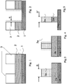
- a portion of a semiconductor electronic circuit comprising a semiconductor substrate 1 on which a layer 2 of a material to be defined is formed.
- a layer 3 of photosensitive material is deposited on the layer 2 of material to be defined, and is then selectively removed by using a conventional photolithographic technique so as to expose the areas of the layer 2 to be defined etched.
- An anisotropic etching is used for the purpose, wherein the wafer in which the electronic device has to be integrated is subjected to a flow of plasma (low-pressure ionized gas).
- a complex chemio-physical process allows to obtain a process where the lengthwise etching component is absolutely predominating over the transversal T one.
- the method, called Resist trimming, is used for forming a circuit structure, typically of polycrystalline silicon, which has a cross-dimension much smaller than that of the corresponding photosensitive layer.
- a layer 2a of a material to be defined is formed on a semiconductor layer 1a.
- a layer of a photosensitive material being deposited and then selectively removed through conventional photolithographic techniques, as shown in Figure 3 , to produce a strip 3a of width S.
- a heavily isotropic etching step is then carried out on the strip 3a. This etching step then thins the strip 3a sideways as shown in Figure 4 , so that, after etching, the strip 3a exhibits a smaller width S' than its original width S.
- the photosensitive layer strip 3a is then etched anisotropically to define a strip 2a' in the underlying material layer 2a of width S'.
- this first solution only allows the size of a lithographed structure to be reduced, but it is not suitable to reduce the distance between two or more structures.
- Another solution employed for providing an opening between two or more adjacent circuit structures rather than for reducing the size of a circuit structure, comprises forming spacers (Spacers formation).
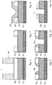
- a layer 2b of a material to be defined and a layer 3b of auxiliary material are formed on a semiconductor substrate 2b.
- a layer 4b of a photosensitive material is then deposited to permit a selective action by the layer 3b of auxiliary material and provide a first window having dimension L.
- a layer 5b is then deposited for defining spacers 6b that are effective to reduce the cross-dimension of the window previously made in the layer 3b, thus reducing the exposed area of the layer 2b to be defined.
- the layer 2b is then etched anisotropically to make a second window L' of a smaller size than the lithographic starting one.
- this method for manufacturing spacers narrowing a window previously defined by lithography has some drawbacks because of the complex circuit architecture made of a succession of depositions and etchings (both isotropic and anisotropic).
- the precision with which the width of the spacers can be controlled has strict limits.
- the spacer dimensions depend on the characteristics of the previous and following steps with respect to their formation (thickness of the layers used, duration of wet etching, etc.). Accordingly, the accuracy of dimensional control after opening the second window is likely to drop to unsatisfactory levels.
- the underlying technical problem of this invention is to provide a method for transferring a lithographic pattern onto a layer directly underneath, such that an opening can be made in a substrate to be defined which is much smaller than the opening obtained through a conventional lithographic technique, thus overcoming prior art limits.
- the solving idea on which this invention is based is that of providing an opening in an auxiliary layer formed on a substrate, the opening having flared sidewalls.
- the following vertical etching of the underlying substrate is thus masked by the flared sidewalls of the opening in the auxiliary layer.
- the cross-dimension of the exposed substrate surface are therefore smaller than the dimension of the top edge of the opening in the auxiliary layer. In this way, an opening can be provided in the substrate underlying the auxiliary layer being narrower than that obtained thorough a conventional photolithographic technique.
- the technical problem is solved by a method as defined in the appended independent claim 1 and comprising the following step: removing said area of said auxiliary layer to form a second opening having sloping sidewalls in said auxiliary layer, whose section narrows towards said substrate so that a diameter of a top of said second opening is larger than a diameter of a bottom of said second opening.
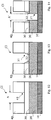
- an integrated circuit CI which has a multi-layer circuit structure comprising of a first layer 10, e.g. a semiconductor substrate; a substrate 20 to be defined; an auxiliary layer 30; and a layer of a screening material, e.g. a photosensitive material 40.
- the word substrate is here used to indicate any layer which supports or underlies another material layer.
- the substrate may be of silicon, polysilicon, metal, or dielectric.
- the layer of photosensitive material 40 is selectively removed through conventional photolithographic techniques to form a first opening 41 having a first width A.
- the auxiliary layer 30 is then anisotropically etched to make an opening 31 with sloping sidewalls, viz. an opening 31 whose vertical section width is not constant and decreases while getting near the substrate 20.
- the opening 31 thus has flared sidewalls, i.e. an inverted trapezium-like shaped cross-section.
- the walls are perfectly straight as shown in the drawings, the walls can be slightly concave or convex as well as irregular or step-like.
- the method of the invention is implemented through chemical etching allowing to obtain a greatly sloping profile of the sidewalls of the opening 31 in the auxiliary layer 30.
- the following vertical etching of the substrate 20 to be defined is thus masked by the flared sidewalls of the opening 31 in the auxiliary layer 30, the sidewalls being flared, and thus reducing the cross-dimension of the exposed surface at the etching step of the substrate to be defined.
- the flare of the sidewalls of the opening 31 is achieved by using chemical plasma etching, wherein an etching component of the auxiliary layer 30 co-exists with a microdeposition component of the various auxiliary layer etching compounds.
- the microdeposition component deposits - on the vertical walls of the opening being formed progressively in the auxiliary layer 30 by means of the etching component - a layer of a so-called polymeric material, thus narrowing the etching area.
- spacers 32 made of this polymeric material are formed in the opening 31 and produce the flared sidewalls.
- the deposition speed of polymer has to be higher than that of etching the auxiliary layer 30, so that the etching direction is leaned with respect to the surface of the substrate 20 and the spacers 32 are formed.
- the ratio between the deposition speed of the polymer on the sidewalls and the etching speed along the lengthwise direction allows to determine the narrowing of the opening 31, i.e. the inclination of the sidewalls of the opening 31 formed by the spacers 32 and the shape of these sidewalls.
- the above ratio may be changed during the auxiliary layer etching step so that the sidewalls of the opening 31 are not perfectly straight but concave or convex.
- the auxiliary layer 30 is an organic layer, e.g. of the polymer type.
- the auxiliary layer 30 comprises an organic material layer known as BARC (Bottom Anti-Reflection Coating).
- BARC Bottom Anti-Reflection Coating
- This BARC layer inhibits exposure of the photosensitive layer 40 (resist) to "back" radiation, i.e. radiation being reflected from the substrate, which would harm the quality of the lithographic definition.
- the thickness of the BARC layer is of 300 to 1500 ⁇ , and its chemical structure is the same as that of a photosensitive layer, except that it undergoes no alterations while being exposed.
- the BARC layer acts as an added layer, to be etched before the substrate 20 to be defined can be etched; it is then automatically removed automatically as the photosensitive layer (resist) is removed.
- the step of etching the auxiliary layer 30, whether a BARC or another organic material layer is carried out by using a plasma which comprises a CF 4 /CH 2 F 2 /O 2 solution.
- the CH 2 F 2 component forms the deposition component for the spacers 32, and the CF 4 /O 2 solution forms the auxiliary layer 30 removing component.
- O 2 concentration varies between 10 sccm and 50 sccm (standard cubic centimetres); CH 2 F 2 concentration between 10 sccm and about 200 sccm; and CF 4 concentration is about 30 sccm.
- Pressure is within the range of 5 mt to 15 mt (milliTorrs) and temperature in the range of 0° to 80°C.
- the CH 2 F 2 deposition component deposits a polymer onto the sidewalls of the opening 31, thus forming the spacers 32 and narrowing the cross-section of the opening 31.
- the spacers are formed with highly selective materials with respect to the substrate 20, so that the size of the opening 31 can be retained through the next step of etching of the substrate 20.
- the method of the invention is particularly advantageous to form the floating gate region of a flash memory cell and all circuit structures being highly thickened in the circuit layout.
- a cross-dimension of the opening 21 in the substrate 20 can be obtained and be greatly reduced if compared to the size of the opening 41 provided in the photosensitive layer 41.
- the cross-dimension A' of the opening 21 provided in the substrate 20 by the method of the invention may be at least 80% smaller than the cross-dimension A of the opening 41 of the photosensitive layer 40.
- the width A' may be 80 nm or less when the method of the invention is used, according to the formula A' ⁇ 0.8A.
- the method of this invention has a number of advantages over the prior art.
- the method of the invention is a comprehensive method in the sense that it can be applied to any circuit structure to be defined as STI structures or floating gate regions, for any kind of substrate (insulating or conductive), by introducing in the photolithographic process an auxiliary layer, such as an organic anti-reflection layer.
- the method of the invention comprises a single conventional plasma etching step, thus lowering the rate of probable defects in the manufacturing process.
- the width, and hence the narrowing, of the exposed area of the layer to be defined can be adjusted.
- the method of the invention keeps manufacturing costs below those of current methods by reducing the number of steps to be carried out.
Landscapes
- Drying Of Semiconductors (AREA)
- Testing Or Measuring Of Semiconductors Or The Like (AREA)
Description
- The present invention relates to a method for manufacturing electronic circuits integrated on a semiconductor substrate.
- The invention further relates to a method for manufacturing semiconductor-integrated electronic circuits comprising the steps of:
- depositing an auxiliary layer on a substrate;
- depositing a layer of screening material on said auxiliary layer;
- selectively removing said layer of screening material to provide a first opening in said layer of screening material and expose an area of said auxiliary layer.
- In particular, though not limited to, the invention relates to a method for defining circuit structures of submicron size, wherein the distance between two or more of them is smaller than the distance provided by a conventional photolithographic process and the following description refers to this field of application for convenience of explanation only.
- As it is well known, one of the basic technological steps for manufacturing integrated circuits is that of transferring some geometries defined by a photosensitive layer (photoresist) on one or more underlying layers: this process is generally called etching step of the layer to be defined.
- It is also known how microelectronics has been subjected for years to a general trend providing a continuous size reduction of the various circuit structures forming the integrated circuit. As the size in the photosensitive layers is critical, the different layer etching step has to reproduce sizes without distortions, i.e. the underlying material has to be etched only along a direction being perpendicular to the substrate.
- With reference in particular to
Figures 1 and 2 , a portion of a semiconductor electronic circuit is shown, comprising asemiconductor substrate 1 on which alayer 2 of a material to be defined is formed. Alayer 3 of photosensitive material is deposited on thelayer 2 of material to be defined, and is then selectively removed by using a conventional photolithographic technique so as to expose the areas of thelayer 2 to be defined etched. An anisotropic etching is used for the purpose, wherein the wafer in which the electronic device has to be integrated is subjected to a flow of plasma (low-pressure ionized gas). A complex chemio-physical process allows to obtain a process where the lengthwise etching component is absolutely predominating over the transversal T one. - Some methods have been studied to obtain circuit structures being smaller than those obtained through a photolithographic process.
- A first prior art solution for obtaining circuit structures in the substrate whose cross-dimension after the etching step is different from that of the photosensitive layer, or anyway allowing to obtain in a layer some circuit structures being smaller than those attainable through a conventional photolithographic process, is illustrated by
Figures 3 to 5 . The method, called Resist trimming, is used for forming a circuit structure, typically of polycrystalline silicon, which has a cross-dimension much smaller than that of the corresponding photosensitive layer. - In particular, a layer 2a of a material to be defined is formed on a semiconductor layer 1a. This is followed by a layer of a photosensitive material being deposited and then selectively removed through conventional photolithographic techniques, as shown in
Figure 3 , to produce astrip 3a of width S. A heavily isotropic etching step is then carried out on thestrip 3a. This etching step then thins thestrip 3a sideways as shown inFigure 4 , so that, after etching, thestrip 3a exhibits a smaller width S' than its original width S. Thephotosensitive layer strip 3a is then etched anisotropically to define a strip 2a' in the underlying material layer 2a of width S'. - Although advantageous into many respects, this first solution only allows the size of a lithographed structure to be reduced, but it is not suitable to reduce the distance between two or more structures.
- Another solution, employed for providing an opening between two or more adjacent circuit structures rather than for reducing the size of a circuit structure, comprises forming spacers (Spacers formation).
- As shown in
Figures 6 to 11 , alayer 2b of a material to be defined and alayer 3b of auxiliary material are formed on asemiconductor substrate 2b. Alayer 4b of a photosensitive material is then deposited to permit a selective action by thelayer 3b of auxiliary material and provide a first window having dimension L. - A
layer 5b is then deposited for defining spacers 6b that are effective to reduce the cross-dimension of the window previously made in thelayer 3b, thus reducing the exposed area of thelayer 2b to be defined. - The
layer 2b is then etched anisotropically to make a second window L' of a smaller size than the lithographic starting one. - While being advantageous from various points of view, this method for manufacturing spacers narrowing a window previously defined by lithography, has some drawbacks because of the complex circuit architecture made of a succession of depositions and etchings (both isotropic and anisotropic).
- In particular, the large number of depositions and etchings greatly worsen the final defect rate of the circuit structure to be realized. In general, particle contaminations deteriorate and heavily worsen the electric characteristics of an integrated circuit. This contamination is partly in the atmosphere, but it is introduced, to a great extent, during each of the process steps for manufacturing the integrated device (masking, depositing, cleaning, etching, etc.).
- In addition, the precision with which the width of the spacers can be controlled has strict limits. Actually the spacer dimensions depend on the characteristics of the previous and following steps with respect to their formation (thickness of the layers used, duration of wet etching, etc.). Accordingly, the accuracy of dimensional control after opening the second window is likely to drop to unsatisfactory levels.
- Furthermore, manufacturing costs grow in proportion to the number of operations involved.
- A method for etching a contact for forming a contact hole having sidewall profile is disclosed in the
US Patent No. 6,040,247 A in the name of the LG Semicon Co.. - An other method of fabricating contact holes for integrated circuit defining a sidewall and concurrently forming a polymer on the sidewall is disclosed in the
US Patent No. 6,028,001 A in the name of the Samsung Electronics Co.. - The underlying technical problem of this invention is to provide a method for transferring a lithographic pattern onto a layer directly underneath, such that an opening can be made in a substrate to be defined which is much smaller than the opening obtained through a conventional lithographic technique, thus overcoming prior art limits.
- The solving idea on which this invention is based is that of providing an opening in an auxiliary layer formed on a substrate, the opening having flared sidewalls. The following vertical etching of the underlying substrate is thus masked by the flared sidewalls of the opening in the auxiliary layer. The cross-dimension of the exposed substrate surface are therefore smaller than the dimension of the top edge of the opening in the auxiliary layer. In this way, an opening can be provided in the substrate underlying the auxiliary layer being narrower than that obtained thorough a conventional photolithographic technique.
- On the basis of this idea, the technical problem is solved by a method as defined in the appended
independent claim 1 and comprising the following step: removing said area of said auxiliary layer to form a second opening having sloping sidewalls in said auxiliary layer, whose section narrows towards said substrate so that a diameter of a top of said second opening is larger than a diameter of a bottom of said second opening. - The features and advantages of the method of this invention should be more clearly understood from the following description of an embodiment thereof, given by way of non limitative example with reference to the accompanying drawings.
- In the drawings:
-
Figures 1 and 2 are cross-sections of a portion of an integrated circuit depicted through successive steps of a first manufacturing method according to the prior art; -
Figures 3, 4 and 5 are cross-sections of a portion of an integrated circuit depicted through successive steps of a second manufacturing method according to the prior art; -
Figures 6 to 11 are cross-sections of a portion of an integrated circuit depicted through successive steps of a third manufacturing method according to the prior art; -
Figures 12, 13 and 14 are cross-sections of a portion of an integrated circuit depicted through successive steps of a manufacturing method according to the invention; and -
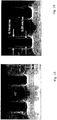
Figures 15 and 16 are SEM micrographs of semiconductor devices as manufactured according to the method of the invention. - The process steps hereinafter described are not exhaustive of an integrated circuit manufacturing process. The invention can be implemented along with conventional integrated circuit manufacturing techniques, and only those conventional steps necessary for an understanding of the invention will be described.
- The cross-sectional views of portions of an integrated circuit while being manufactured have not been drawn to scale but so as to emphasize major features of the invention.
- Referring to
Figures 12 to 14 , an integrated circuit CI is shown which has a multi-layer circuit structure comprising of afirst layer 10, e.g. a semiconductor substrate; asubstrate 20 to be defined; anauxiliary layer 30; and a layer of a screening material, e.g. aphotosensitive material 40. - The word substrate is here used to indicate any layer which supports or underlies another material layer. The substrate may be of silicon, polysilicon, metal, or dielectric.
- In the method of this invention, the layer of
photosensitive material 40 is selectively removed through conventional photolithographic techniques to form afirst opening 41 having a first width A. - According to the invention, the
auxiliary layer 30 is then anisotropically etched to make an opening 31 with sloping sidewalls, viz. anopening 31 whose vertical section width is not constant and decreases while getting near thesubstrate 20. - The
opening 31 thus has flared sidewalls, i.e. an inverted trapezium-like shaped cross-section. - Although the sidewalls are perfectly straight as shown in the drawings, the walls can be slightly concave or convex as well as irregular or step-like.
- Thus, subsequent etching of the
substrate 20 to be defined is then screened by the flared sidewalls of theopening 31 in theauxiliary layer 30, reducing cross dimension of the etching surface as well as the cross-dimension A' of theopening 21 which is then formed in thesubstrate 20 to be defined. - Advantageously, the method of the invention is implemented through chemical etching allowing to obtain a greatly sloping profile of the sidewalls of the
opening 31 in theauxiliary layer 30. The following vertical etching of thesubstrate 20 to be defined is thus masked by the flared sidewalls of theopening 31 in theauxiliary layer 30, the sidewalls being flared, and thus reducing the cross-dimension of the exposed surface at the etching step of the substrate to be defined. - Advantageously, the flare of the sidewalls of the
opening 31 is achieved by using chemical plasma etching, wherein an etching component of theauxiliary layer 30 co-exists with a microdeposition component of the various auxiliary layer etching compounds. The microdeposition component deposits - on the vertical walls of the opening being formed progressively in theauxiliary layer 30 by means of the etching component - a layer of a so-called polymeric material, thus narrowing the etching area. In this way while theauxiliary layer 30 is being etched,spacers 32 made of this polymeric material are formed in theopening 31 and produce the flared sidewalls. - In particular, on the vertical side surfaces of the
opening 31, the deposition speed of polymer has to be higher than that of etching theauxiliary layer 30, so that the etching direction is leaned with respect to the surface of thesubstrate 20 and thespacers 32 are formed. - Advantageously in the method of the invention, the ratio between the deposition speed of the polymer on the sidewalls and the etching speed along the lengthwise direction (together with the thickness of the auxiliary layer 30) allows to determine the narrowing of the
opening 31, i.e. the inclination of the sidewalls of theopening 31 formed by thespacers 32 and the shape of these sidewalls. - In particular, the above ratio may be changed during the auxiliary layer etching step so that the sidewalls of the
opening 31 are not perfectly straight but concave or convex. - Advantageously in the invention, the
auxiliary layer 30 is an organic layer, e.g. of the polymer type. - In a modified embodiment of the inventive method, the
auxiliary layer 30 comprises an organic material layer known as BARC (Bottom Anti-Reflection Coating). This BARC layer inhibits exposure of the photosensitive layer 40 (resist) to "back" radiation, i.e. radiation being reflected from the substrate, which would harm the quality of the lithographic definition. The thickness of the BARC layer is of 300 to 1500 Å, and its chemical structure is the same as that of a photosensitive layer, except that it undergoes no alterations while being exposed. Thus, during theauxiliary layer 30 etching, the BARC layer acts as an added layer, to be etched before thesubstrate 20 to be defined can be etched; it is then automatically removed automatically as the photosensitive layer (resist) is removed. - Advantageously in this invention, the step of etching the
auxiliary layer 30, whether a BARC or another organic material layer, is carried out by using a plasma which comprises a CF4/CH2F2/O2 solution. - In particular, the CH2F2 component forms the deposition component for the
spacers 32, and the CF4/O2 solution forms theauxiliary layer 30 removing component. - In one embodiment of the manufacturing method of the invention, O2 concentration varies between 10 sccm and 50 sccm (standard cubic centimetres); CH2F2 concentration between 10 sccm and about 200 sccm; and CF4 concentration is about 30 sccm. Pressure is within the range of 5 mt to 15 mt (milliTorrs) and temperature in the range of 0° to 80°C. As said before, during the etching step, the CH2F2 deposition component deposits a polymer onto the sidewalls of the
opening 31, thus forming thespacers 32 and narrowing the cross-section of theopening 31. - Advantageously, the spacers are formed with highly selective materials with respect to the
substrate 20, so that the size of theopening 31 can be retained through the next step of etching of thesubstrate 20. - In fact consumption of the
spacers 32, and so of the sidewalls of theopening 31, during thesubstrate 20 etching would lead, because of the flaredopening 31 shape, to a gradual increase of the exposure cross-dimension of thesubstrate 20, thus causing a not perfectly vertical shape or anyway distorted. - There is no reason, however, why the method of the invention could not be implemented by using polymerizing gases different from CH2F2, such as CHF3 or else.
- The method of the invention is particularly advantageous to form the floating gate region of a flash memory cell and all circuit structures being highly thickened in the circuit layout.
- In particular, through the method of the invention, a cross-dimension of the
opening 21 in thesubstrate 20 can be obtained and be greatly reduced if compared to the size of theopening 41 provided in thephotosensitive layer 41. - Advantageously, the cross-dimension A' of the
opening 21 provided in thesubstrate 20 by the method of the invention may be at least 80% smaller than the cross-dimension A of theopening 41 of thephotosensitive layer 40. - As an example, assuming a width A of 100 nm, the width A' may be 80 nm or less when the method of the invention is used, according to the formula A' < 0.8A.
- Tests carried out by the Applicant's have shown that openings made with the method of the invention, e.g. among the floating gate regions of flash memory cells, allow to achieve a reduction in cross-dimension of 60 to 70 nm with respect to conventional techniques, as illustrated in
Figures 15 and 16 . - These drawings show that a size of 0.14 µm of the opening made in the photosenstive layer drops to a size of 0.08 µm of the exposed area of the polysilicon layer.
- In conclusion, the method of this invention has a number of advantages over the prior art.
- In particular, the method of the invention is a comprehensive method in the sense that it can be applied to any circuit structure to be defined as STI structures or floating gate regions, for any kind of substrate (insulating or conductive), by introducing in the photolithographic process an auxiliary layer, such as an organic anti-reflection layer.
- Unlike conventional methods which are based on a sequence of depositing and etching steps, the method of the invention comprises a single conventional plasma etching step, thus lowering the rate of probable defects in the manufacturing process.
- Moreover, by changing certain parameters of the plasma employed to etch the substrate to be defined, the width, and hence the narrowing, of the exposed area of the layer to be defined can be adjusted.
- Finally, the method of the invention keeps manufacturing costs below those of current methods by reducing the number of steps to be carried out.
Claims (11)
- A method of semiconductor manufacturing comprising the steps of:depositing an auxiliary layer (30) on a substrate layer (20);depositing a layer (40) of a screening material on to said auxiliary layer (30); andselectively removing said layer (40) of screening material to provide a first opening (41) in said layer (40) of screening material and to expose an area of said auxiliary layer (30);removing said area of said auxiliary layer to form a second opening (31) having sloping sidewalls in said auxiliary layer (30), the second opening (31) having a cross-section that narrows toward said substrate (20) so that a diameter (A) of a top of said second opening (31) is larger than a diameter (A') of a bottom of said second opening (31);vertically etching the substrate layer (20) to form a third opening (21) in the substrate layer (20) using the spacers (32) to mask the etching of the substrate layer (20);wherein forming said second opening (31) in said auxiliary layer (30) includes simultaneously removing said auxiliary layer (3) and forming the spacers (32), said spacers (32) forming the sloping sidewalls of the second opening (31), andwherein said auxiliary layer (30) is removed through an anisotropic plasma etch that includes a component for removing said auxiliary layer (30) and a component for depositing said spacers (32).
- A method according to Claim 1, characterized in that said second opening (31) in said auxiliary layer (30) has flared sidewalls.
- A method according to Claim 2, characterized in that the deposition speed on the side surfaces of the opening (31) is higher than the etching speed.
- A method according to Claim 1, characterized in that said spacers (32) are formed with a highly selective material with respect to said substrate (20).
- A method according to Claim 1, characterized in that said spacers (32) are formed with polymeric organic material.
- A method according to Claim 1, characterized in that said auxiliary layer (30) comprises organic material.
- A method according to Claim 6, characterized in that said layer (30) comprises polymeric organic material.
- A method according to Claim 7, characterized in that said layer (30) of polymeric organic material comprises BARC (Bottom Anti-Reflection Coating).
- A method according to Claim 1, characterized in that said plasma etching comprises a CF4/CH2F2/O2 solution.
- A method according to Claim 9, characterized in that said CF4/CH2F2/O2 solution comprises a deposition component consisting essentially of CH2F2 and an etching component essentially regulated by CF4 and 02.
- A method according to Claim 1, characterized in that the width (A') of the exposed area of said substrate (20) through said second opening (31) in said auxiliary layer (30) is 80% smaller than the width (A) of said first opening (41) in said layer (40) of screening material.
Applications Claiming Priority (2)
| Application Number | Priority Date | Filing Date | Title |
|---|---|---|---|
| ITMI20020931 | 2002-05-02 | ||
| IT2002MI000931A ITMI20020931A1 (en) | 2002-05-02 | 2002-05-02 | METHOD FOR MANUFACTURING INTEGRATED ELECTRONIC CIRCUITS ON A SEMICONDUCTIVE SUBSTRATE |
Publications (3)
| Publication Number | Publication Date |
|---|---|
| EP1361603A2 EP1361603A2 (en) | 2003-11-12 |
| EP1361603A3 EP1361603A3 (en) | 2004-04-14 |
| EP1361603B1 true EP1361603B1 (en) | 2019-07-24 |
Family
ID=11449819
Family Applications (1)
| Application Number | Title | Priority Date | Filing Date |
|---|---|---|---|
| EP03009600.2A Expired - Lifetime EP1361603B1 (en) | 2002-05-02 | 2003-04-29 | Method for manufacturing electronic circuits integrated on a semiconductor substrate |
Country Status (3)
| Country | Link |
|---|---|
| US (2) | US6998348B2 (en) |
| EP (1) | EP1361603B1 (en) |
| IT (1) | ITMI20020931A1 (en) |
Families Citing this family (10)
| Publication number | Priority date | Publication date | Assignee | Title |
|---|---|---|---|---|
| ITMI20020931A1 (en) * | 2002-05-02 | 2003-11-03 | St Microelectronics Srl | METHOD FOR MANUFACTURING INTEGRATED ELECTRONIC CIRCUITS ON A SEMICONDUCTIVE SUBSTRATE |
| ITMI20022784A1 (en) | 2002-12-30 | 2004-06-30 | St Microelectronics Srl | PROCESS FOR THE MANUFACTURE OF MEMORY CELLS |
| ITMI20022785A1 (en) | 2002-12-30 | 2004-06-30 | St Microelectronics Srl | PROCESS FOR THE MANUFACTURE OF MEMORY CELLS |
| KR100700283B1 (en) * | 2005-12-28 | 2007-03-26 | 동부일렉트로닉스 주식회사 | Trench Formation for Device Separation in Semiconductor Devices |
| US7838432B2 (en) * | 2007-04-16 | 2010-11-23 | Applied Materials, Inc. | Etch process with controlled critical dimension shrink |
| JP2010041028A (en) | 2008-07-11 | 2010-02-18 | Tokyo Electron Ltd | Substrate processing method |
| JP5180121B2 (en) * | 2009-02-20 | 2013-04-10 | 東京エレクトロン株式会社 | Substrate processing method |
| JP2010283213A (en) * | 2009-06-05 | 2010-12-16 | Tokyo Electron Ltd | Substrate processing method |
| US9229326B2 (en) * | 2014-03-14 | 2016-01-05 | Taiwan Semiconductor Manufacturing Company, Ltd. | Method for integrated circuit patterning |
| WO2017111822A1 (en) * | 2015-12-24 | 2017-06-29 | Intel Corporation | Pitch division using directed self-assembly |
Family Cites Families (27)
| Publication number | Priority date | Publication date | Assignee | Title |
|---|---|---|---|---|
| DE3275447D1 (en) * | 1982-07-03 | 1987-03-19 | Ibm Deutschland | Process for the formation of grooves having essentially vertical lateral silicium walls by reactive ion etching |
| EP0263220B1 (en) * | 1986-10-08 | 1992-09-09 | International Business Machines Corporation | Method of forming a via-having a desired slope in a photoresist masked composite insulating layer |
| AU3927993A (en) * | 1992-03-20 | 1993-10-21 | General Hospital Corporation, The | Laser illuminator |
| US5716494A (en) * | 1992-06-22 | 1998-02-10 | Matsushita Electric Industrial Co., Ltd. | Dry etching method, chemical vapor deposition method, and apparatus for processing semiconductor substrate |
| US6040247A (en) * | 1995-01-10 | 2000-03-21 | Lg Semicon Co., Ltd. | Method for etching contact |
| US5525542A (en) * | 1995-02-24 | 1996-06-11 | Motorola, Inc. | Method for making a semiconductor device having anti-reflective coating |
| US5910453A (en) * | 1996-01-16 | 1999-06-08 | Advanced Micro Devices, Inc. | Deep UV anti-reflection coating etch |
| US5750441A (en) * | 1996-05-20 | 1998-05-12 | Micron Technology, Inc. | Mask having a tapered profile used during the formation of a semiconductor device |
| US5670401A (en) * | 1996-08-22 | 1997-09-23 | Vanguard International Semiconductor Corporation | Method for fabricating a deep submicron mosfet device using an in-situ polymer spacer to decrease device channel length |
| EP0871213A3 (en) * | 1997-03-27 | 1999-03-03 | Siemens Aktiengesellschaft | Method for producing vias having variable sidewall profile |
| US5994228A (en) * | 1997-04-11 | 1999-11-30 | Vanguard International Semiconductor Corporation | Method of fabricating contact holes in high density integrated circuits using taper contact and self-aligned etching processes |
| JP3905232B2 (en) * | 1997-12-27 | 2007-04-18 | 東京エレクトロン株式会社 | Etching method |
| KR100272510B1 (en) * | 1997-12-30 | 2000-12-01 | 김영환 | Contact hole formation method of semiconductor device |
| KR100280622B1 (en) * | 1998-04-02 | 2001-03-02 | 윤종용 | Contact Forming Method of Semiconductor Device |
| US6329292B1 (en) * | 1998-07-09 | 2001-12-11 | Applied Materials, Inc. | Integrated self aligned contact etch |
| US6235214B1 (en) * | 1998-12-03 | 2001-05-22 | Applied Materials, Inc. | Plasma etching of silicon using fluorinated gas mixtures |
| KR100881472B1 (en) * | 1999-02-04 | 2009-02-05 | 어플라이드 머티어리얼스, 인코포레이티드 | A method for depositing a stacked structure over a patterned mask surface lying on a given substrate |
| US6693038B1 (en) * | 1999-02-05 | 2004-02-17 | Taiwan Semiconductor Manufacturing Company | Method for forming electrical contacts through multi-level dielectric layers by high density plasma etching |
| US6335292B1 (en) * | 1999-04-15 | 2002-01-01 | Micron Technology, Inc. | Method of controlling striations and CD loss in contact oxide etch |
| US6431182B1 (en) * | 1999-10-27 | 2002-08-13 | Advanced Micro Devices, Inc. | Plasma treatment for polymer removal after via etch |
| US6326307B1 (en) * | 1999-11-15 | 2001-12-04 | Appllied Materials, Inc. | Plasma pretreatment of photoresist in an oxide etch process |
| US20010024769A1 (en) * | 2000-02-08 | 2001-09-27 | Kevin Donoghue | Method for removing photoresist and residues from semiconductor device surfaces |
| US6649517B2 (en) * | 2001-05-18 | 2003-11-18 | Chartered Semiconductor Manufacturing Ltd. | Copper metal structure for the reduction of intra-metal capacitance |
| JP2002353195A (en) * | 2001-05-23 | 2002-12-06 | Sony Corp | Method for manufacturing semiconductor device |
| US6732411B2 (en) * | 2001-05-23 | 2004-05-11 | Michael A. Vidal | Hand tool handle modification system |
| US6699792B1 (en) * | 2001-07-17 | 2004-03-02 | Advanced Micro Devices, Inc. | Polymer spacers for creating small geometry space and method of manufacture thereof |
| ITMI20020931A1 (en) * | 2002-05-02 | 2003-11-03 | St Microelectronics Srl | METHOD FOR MANUFACTURING INTEGRATED ELECTRONIC CIRCUITS ON A SEMICONDUCTIVE SUBSTRATE |
-
2002
- 2002-05-02 IT IT2002MI000931A patent/ITMI20020931A1/en unknown
-
2003
- 2003-04-29 EP EP03009600.2A patent/EP1361603B1/en not_active Expired - Lifetime
- 2003-05-01 US US10/428,338 patent/US6998348B2/en not_active Expired - Fee Related
-
2005
- 2005-12-06 US US11/294,763 patent/US20060073651A1/en not_active Abandoned
Non-Patent Citations (1)
| Title |
|---|
| None * |
Also Published As
| Publication number | Publication date |
|---|---|
| US20040029307A1 (en) | 2004-02-12 |
| EP1361603A2 (en) | 2003-11-12 |
| US20060073651A1 (en) | 2006-04-06 |
| EP1361603A3 (en) | 2004-04-14 |
| ITMI20020931A1 (en) | 2003-11-03 |
| ITMI20020931A0 (en) | 2002-05-02 |
| US6998348B2 (en) | 2006-02-14 |
Similar Documents
| Publication | Publication Date | Title |
|---|---|---|
| US9082721B2 (en) | Structures comprising masks comprising carbon | |
| US7271106B2 (en) | Critical dimension control for integrated circuits | |
| US8294278B2 (en) | Methods for pitch reduction | |
| US7494934B2 (en) | Method of etching carbon-containing layer and method of fabricating semiconductor device | |
| CN1090815C (en) | Method of forming cavity and contact window | |
| US6716761B2 (en) | Method of forming fine patterns | |
| US6653058B2 (en) | Methods for reducing profile variation in photoresist trimming | |
| US6291137B1 (en) | Sidewall formation for sidewall patterning of sub 100 nm structures | |
| US6849556B2 (en) | Etching method, gate etching method, and method of manufacturing semiconductor devices | |
| US20040051183A1 (en) | Method of forming self-aligned contact structure with locally etched gate conductive layer | |
| US6423475B1 (en) | Sidewall formation for sidewall patterning of sub 100 nm structures | |
| US20040053490A1 (en) | Semiconductor device manufacturing method | |
| US6579808B2 (en) | Method of fabricating a semiconductor device | |
| US6998348B2 (en) | Method for manufacturing electronic circuits integrated on a semiconductor substrate | |
| US6399286B1 (en) | Method of fabricating reduced critical dimension for conductive line and space | |
| US7015136B2 (en) | Method for preventing formation of photoresist scum | |
| US7060628B2 (en) | Method for fabricating a hard mask polysilicon gate | |
| US6214737B1 (en) | Simplified sidewall formation for sidewall patterning of sub 100 nm structures | |
| JPH05121371A (en) | Method of manufacturing semiconductor device | |
| KR100495909B1 (en) | Method for fabrication of semiconductor device using ArF photo-lithography capable of protecting tapered profile of hardmask | |
| KR100466192B1 (en) | Method for manufacturing semiconductor device | |
| KR101073127B1 (en) | Method for manufacturing gate-line in semiconductor device | |
| KR20050001186A (en) | Method for filling gap in fabrication of semiconductor device | |
| KR20030093715A (en) | Method for fabricating semiconductor device | |
| KR19990053222A (en) | Fine conductive film pattern formation method of semiconductor device |
Legal Events
| Date | Code | Title | Description |
|---|---|---|---|
| PUAI | Public reference made under article 153(3) epc to a published international application that has entered the european phase |
Free format text: ORIGINAL CODE: 0009012 |
|
| AK | Designated contracting states |
Kind code of ref document: A2 Designated state(s): AT BE BG CH CY CZ DE DK EE ES FI FR GB GR HU IE IT LI LU MC NL PT RO SE SI SK TR |
|
| AX | Request for extension of the european patent |
Extension state: AL LT LV MK |
|
| PUAL | Search report despatched |
Free format text: ORIGINAL CODE: 0009013 |
|
| AK | Designated contracting states |
Kind code of ref document: A3 Designated state(s): AT BE BG CH CY CZ DE DK EE ES FI FR GB GR HU IE IT LI LU MC NL PT RO SE SI SK TR |
|
| AX | Request for extension of the european patent |
Extension state: AL LT LV MK |
|
| RIC1 | Information provided on ipc code assigned before grant |
Ipc: 7H 01L 21/3065 A Ipc: 7H 01L 21/027 B Ipc: 7H 01L 21/3213 B Ipc: 7H 01L 21/768 B Ipc: 7H 01L 21/311 B |
|
| 17P | Request for examination filed |
Effective date: 20040513 |
|
| AKX | Designation fees paid |
Designated state(s): DE FR GB IT |
|
| RAP1 | Party data changed (applicant data changed or rights of an application transferred) |
Owner name: STMICROELECTRONICS SRL |
|
| RAP1 | Party data changed (applicant data changed or rights of an application transferred) |
Owner name: STMICROELECTRONICS SRL |
|
| RAP1 | Party data changed (applicant data changed or rights of an application transferred) |
Owner name: MICRON TECHNOLOGY, INC. |
|
| GRAP | Despatch of communication of intention to grant a patent |
Free format text: ORIGINAL CODE: EPIDOSNIGR1 |
|
| STAA | Information on the status of an ep patent application or granted ep patent |
Free format text: STATUS: GRANT OF PATENT IS INTENDED |
|
| INTG | Intention to grant announced |
Effective date: 20190131 |
|
| RIN1 | Information on inventor provided before grant (corrected) |
Inventor name: COLOMBO, ROBERTO Inventor name: ALBA, SIMONE Inventor name: CIOVACCO, FRANCESCO Inventor name: SAVARDI, CHIARA |
|
| GRAS | Grant fee paid |
Free format text: ORIGINAL CODE: EPIDOSNIGR3 |
|
| GRAA | (expected) grant |
Free format text: ORIGINAL CODE: 0009210 |
|
| STAA | Information on the status of an ep patent application or granted ep patent |
Free format text: STATUS: THE PATENT HAS BEEN GRANTED |
|
| AK | Designated contracting states |
Kind code of ref document: B1 Designated state(s): DE FR GB IT |
|
| REG | Reference to a national code |
Ref country code: GB Ref legal event code: FG4D |
|
| REG | Reference to a national code |
Ref country code: DE Ref legal event code: R096 Ref document number: 60352147 Country of ref document: DE |
|
| PG25 | Lapsed in a contracting state [announced via postgrant information from national office to epo] |
Ref country code: IT Free format text: LAPSE BECAUSE OF FAILURE TO SUBMIT A TRANSLATION OF THE DESCRIPTION OR TO PAY THE FEE WITHIN THE PRESCRIBED TIME-LIMIT Effective date: 20190724 |
|
| REG | Reference to a national code |
Ref country code: DE Ref legal event code: R097 Ref document number: 60352147 Country of ref document: DE |
|
| PLBE | No opposition filed within time limit |
Free format text: ORIGINAL CODE: 0009261 |
|
| STAA | Information on the status of an ep patent application or granted ep patent |
Free format text: STATUS: NO OPPOSITION FILED WITHIN TIME LIMIT |
|
| 26N | No opposition filed |
Effective date: 20200603 |
|
| PG25 | Lapsed in a contracting state [announced via postgrant information from national office to epo] |
Ref country code: FR Free format text: LAPSE BECAUSE OF NON-PAYMENT OF DUE FEES Effective date: 20200430 |
|
| GBPC | Gb: european patent ceased through non-payment of renewal fee |
Effective date: 20200429 |
|
| PG25 | Lapsed in a contracting state [announced via postgrant information from national office to epo] |
Ref country code: GB Free format text: LAPSE BECAUSE OF NON-PAYMENT OF DUE FEES Effective date: 20200429 |
|
| PGFP | Annual fee paid to national office [announced via postgrant information from national office to epo] |
Ref country code: DE Payment date: 20220527 Year of fee payment: 20 |
|
| REG | Reference to a national code |
Ref country code: DE Ref legal event code: R071 Ref document number: 60352147 Country of ref document: DE |