EP1361560A2 - Semiconductor driver circuit, display device and method of adjusting brightness balance for display device - Google Patents
Semiconductor driver circuit, display device and method of adjusting brightness balance for display device Download PDFInfo
- Publication number
- EP1361560A2 EP1361560A2 EP03010211A EP03010211A EP1361560A2 EP 1361560 A2 EP1361560 A2 EP 1361560A2 EP 03010211 A EP03010211 A EP 03010211A EP 03010211 A EP03010211 A EP 03010211A EP 1361560 A2 EP1361560 A2 EP 1361560A2
- Authority
- EP
- European Patent Office
- Prior art keywords
- output
- driver circuit
- semiconductor
- output bump
- electrodes
- Prior art date
- Legal status (The legal status is an assumption and is not a legal conclusion. Google has not performed a legal analysis and makes no representation as to the accuracy of the status listed.)
- Withdrawn
Links
- 239000004065 semiconductor Substances 0.000 title claims abstract description 43
- 238000000034 method Methods 0.000 title claims description 10
- 239000003086 colorant Substances 0.000 claims description 14
- 239000012780 transparent material Substances 0.000 claims description 8
- 239000002019 doping agent Substances 0.000 claims description 3
- AMGQUBHHOARCQH-UHFFFAOYSA-N indium;oxotin Chemical compound [In].[Sn]=O AMGQUBHHOARCQH-UHFFFAOYSA-N 0.000 claims description 2
- 238000010586 diagram Methods 0.000 description 16
- 238000005538 encapsulation Methods 0.000 description 6
- 230000000694 effects Effects 0.000 description 4
- 239000000463 material Substances 0.000 description 4
- 239000000758 substrate Substances 0.000 description 4
- 238000002834 transmittance Methods 0.000 description 3
- 238000000295 emission spectrum Methods 0.000 description 2
- RYGMFSIKBFXOCR-UHFFFAOYSA-N Copper Chemical compound [Cu] RYGMFSIKBFXOCR-UHFFFAOYSA-N 0.000 description 1
- 229910052782 aluminium Inorganic materials 0.000 description 1
- XAGFODPZIPBFFR-UHFFFAOYSA-N aluminium Chemical compound [Al] XAGFODPZIPBFFR-UHFFFAOYSA-N 0.000 description 1
- 230000000903 blocking effect Effects 0.000 description 1
- 238000006243 chemical reaction Methods 0.000 description 1
- 229910052802 copper Inorganic materials 0.000 description 1
- 239000010949 copper Substances 0.000 description 1
- 239000011521 glass Substances 0.000 description 1
- 239000011159 matrix material Substances 0.000 description 1
- 229910052751 metal Inorganic materials 0.000 description 1
- 239000002184 metal Substances 0.000 description 1
- 150000002894 organic compounds Chemical class 0.000 description 1
- 238000001228 spectrum Methods 0.000 description 1
Images


Classifications
-
- G—PHYSICS
- G09—EDUCATION; CRYPTOGRAPHY; DISPLAY; ADVERTISING; SEALS
- G09G—ARRANGEMENTS OR CIRCUITS FOR CONTROL OF INDICATING DEVICES USING STATIC MEANS TO PRESENT VARIABLE INFORMATION
- G09G3/00—Control arrangements or circuits, of interest only in connection with visual indicators other than cathode-ray tubes
- G09G3/20—Control arrangements or circuits, of interest only in connection with visual indicators other than cathode-ray tubes for presentation of an assembly of a number of characters, e.g. a page, by composing the assembly by combination of individual elements arranged in a matrix no fixed position being assigned to or needed to be assigned to the individual characters or partial characters
- G09G3/22—Control arrangements or circuits, of interest only in connection with visual indicators other than cathode-ray tubes for presentation of an assembly of a number of characters, e.g. a page, by composing the assembly by combination of individual elements arranged in a matrix no fixed position being assigned to or needed to be assigned to the individual characters or partial characters using controlled light sources
- G09G3/30—Control arrangements or circuits, of interest only in connection with visual indicators other than cathode-ray tubes for presentation of an assembly of a number of characters, e.g. a page, by composing the assembly by combination of individual elements arranged in a matrix no fixed position being assigned to or needed to be assigned to the individual characters or partial characters using controlled light sources using electroluminescent panels
-
- G—PHYSICS
- G09—EDUCATION; CRYPTOGRAPHY; DISPLAY; ADVERTISING; SEALS
- G09G—ARRANGEMENTS OR CIRCUITS FOR CONTROL OF INDICATING DEVICES USING STATIC MEANS TO PRESENT VARIABLE INFORMATION
- G09G3/00—Control arrangements or circuits, of interest only in connection with visual indicators other than cathode-ray tubes
- G09G3/20—Control arrangements or circuits, of interest only in connection with visual indicators other than cathode-ray tubes for presentation of an assembly of a number of characters, e.g. a page, by composing the assembly by combination of individual elements arranged in a matrix no fixed position being assigned to or needed to be assigned to the individual characters or partial characters
- G09G3/22—Control arrangements or circuits, of interest only in connection with visual indicators other than cathode-ray tubes for presentation of an assembly of a number of characters, e.g. a page, by composing the assembly by combination of individual elements arranged in a matrix no fixed position being assigned to or needed to be assigned to the individual characters or partial characters using controlled light sources
- G09G3/30—Control arrangements or circuits, of interest only in connection with visual indicators other than cathode-ray tubes for presentation of an assembly of a number of characters, e.g. a page, by composing the assembly by combination of individual elements arranged in a matrix no fixed position being assigned to or needed to be assigned to the individual characters or partial characters using controlled light sources using electroluminescent panels
- G09G3/32—Control arrangements or circuits, of interest only in connection with visual indicators other than cathode-ray tubes for presentation of an assembly of a number of characters, e.g. a page, by composing the assembly by combination of individual elements arranged in a matrix no fixed position being assigned to or needed to be assigned to the individual characters or partial characters using controlled light sources using electroluminescent panels semiconductive, e.g. using light-emitting diodes [LED]
- G09G3/3208—Control arrangements or circuits, of interest only in connection with visual indicators other than cathode-ray tubes for presentation of an assembly of a number of characters, e.g. a page, by composing the assembly by combination of individual elements arranged in a matrix no fixed position being assigned to or needed to be assigned to the individual characters or partial characters using controlled light sources using electroluminescent panels semiconductive, e.g. using light-emitting diodes [LED] organic, e.g. using organic light-emitting diodes [OLED]
- G09G3/3266—Details of drivers for scan electrodes
-
- G—PHYSICS
- G09—EDUCATION; CRYPTOGRAPHY; DISPLAY; ADVERTISING; SEALS
- G09G—ARRANGEMENTS OR CIRCUITS FOR CONTROL OF INDICATING DEVICES USING STATIC MEANS TO PRESENT VARIABLE INFORMATION
- G09G3/00—Control arrangements or circuits, of interest only in connection with visual indicators other than cathode-ray tubes
- G09G3/20—Control arrangements or circuits, of interest only in connection with visual indicators other than cathode-ray tubes for presentation of an assembly of a number of characters, e.g. a page, by composing the assembly by combination of individual elements arranged in a matrix no fixed position being assigned to or needed to be assigned to the individual characters or partial characters
- G09G3/22—Control arrangements or circuits, of interest only in connection with visual indicators other than cathode-ray tubes for presentation of an assembly of a number of characters, e.g. a page, by composing the assembly by combination of individual elements arranged in a matrix no fixed position being assigned to or needed to be assigned to the individual characters or partial characters using controlled light sources
- G09G3/30—Control arrangements or circuits, of interest only in connection with visual indicators other than cathode-ray tubes for presentation of an assembly of a number of characters, e.g. a page, by composing the assembly by combination of individual elements arranged in a matrix no fixed position being assigned to or needed to be assigned to the individual characters or partial characters using controlled light sources using electroluminescent panels
- G09G3/32—Control arrangements or circuits, of interest only in connection with visual indicators other than cathode-ray tubes for presentation of an assembly of a number of characters, e.g. a page, by composing the assembly by combination of individual elements arranged in a matrix no fixed position being assigned to or needed to be assigned to the individual characters or partial characters using controlled light sources using electroluminescent panels semiconductive, e.g. using light-emitting diodes [LED]
- G09G3/3208—Control arrangements or circuits, of interest only in connection with visual indicators other than cathode-ray tubes for presentation of an assembly of a number of characters, e.g. a page, by composing the assembly by combination of individual elements arranged in a matrix no fixed position being assigned to or needed to be assigned to the individual characters or partial characters using controlled light sources using electroluminescent panels semiconductive, e.g. using light-emitting diodes [LED] organic, e.g. using organic light-emitting diodes [OLED]
- G09G3/3275—Details of drivers for data electrodes
-
- G—PHYSICS
- G09—EDUCATION; CRYPTOGRAPHY; DISPLAY; ADVERTISING; SEALS
- G09G—ARRANGEMENTS OR CIRCUITS FOR CONTROL OF INDICATING DEVICES USING STATIC MEANS TO PRESENT VARIABLE INFORMATION
- G09G2300/00—Aspects of the constitution of display devices
- G09G2300/04—Structural and physical details of display devices
- G09G2300/0421—Structural details of the set of electrodes
- G09G2300/0426—Layout of electrodes and connections
-
- G—PHYSICS
- G09—EDUCATION; CRYPTOGRAPHY; DISPLAY; ADVERTISING; SEALS
- G09G—ARRANGEMENTS OR CIRCUITS FOR CONTROL OF INDICATING DEVICES USING STATIC MEANS TO PRESENT VARIABLE INFORMATION
- G09G2320/00—Control of display operating conditions
- G09G2320/02—Improving the quality of display appearance
- G09G2320/0233—Improving the luminance or brightness uniformity across the screen
-
- G—PHYSICS
- G09—EDUCATION; CRYPTOGRAPHY; DISPLAY; ADVERTISING; SEALS
- G09G—ARRANGEMENTS OR CIRCUITS FOR CONTROL OF INDICATING DEVICES USING STATIC MEANS TO PRESENT VARIABLE INFORMATION
- G09G2320/00—Control of display operating conditions
- G09G2320/02—Improving the quality of display appearance
- G09G2320/0242—Compensation of deficiencies in the appearance of colours
Definitions
- the present invention relates to a semiconductor driver circuit for driving an electroluminescent device through an electrode and to a display device with the semiconductor driver circuit and further to a method for adjusting brightness balance of a display element in the display device.
- a display device with a display element that includes pixels made of electroluminescent devices generally has data electrodes and scanning electrodes.
- the word of "EL” means “electroluminescent” in the following description.
- the data electrodes and the scanning electrodes intersect with each other, and the EL device is connected to both the data electrodes and the scanning electrodes at each intersection.
- the data electrodes are connected to output bumps of a semiconductor data driver circuit.
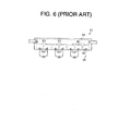
- FIG. 6 the diagram illustrates one of a conventional semiconductor data driver circuit 91.
- the semiconductor data diver 91 includes an input circuit 92.
- a plurality of constant-current driver circuits 93 is connected to the input circuit 92 through electric wirings, which are not shown in the drawing.
- Data electrodes 95 are made of transparent material and are located on the visible side of the EL device.
- the output bumps 94 are arranged in a row near the display element in the semiconductor data driver circuit 91.
- An unwanted feature is that, if an image needs to be displayed in high resolution by the display device, the number of pixels in the display element needs to be increased. As the number of pixels increases, the number of data electrodes 95 for driving the pixels also increases. Accordingly, the size of a chip is enlarged so that the cost may rise. To avoid enlarging the size of the chip, a distance between the coadjacent data electrodes 95, that is, a distance between the coadjacent output bumps 94 needs to be shortened. However, when the output bumps 94 are arranged in a single row, the distance between the output bumps 94 cannot be shorter than the width of the constant-current driver circuit 93.
- the width of the constant-current driver circuit 93 cannot be smaller due to a structure of the circuit 93. This prevents the image from being displayed in high resolution. Therefore, there is a need for a semiconductor driver circuit and a display device that allow a distance between the electrodes to be shortened and also allow the area of a chip to be easily reduced, and in addition there is a need for adjusting brightness balance of a display element in a display device.
- a semiconductor driver circuit has a plurality of output bumps that are connected to respective electrodes and energizes electroluminescent devices through the electrodes.
- the output bumps are arranged in a plurality of output bump rows.
- Each of the output bump rows includes a plurality of output bumps.
- the present invention also provides a method for adjusting brightness balance on a display element of a display device.
- the display element includes electroluminescent devices that are energized by electric current from semiconductor driver circuits through electrodes for displaying a color image.
- the semiconductor driver circuits include a semiconductor data driver circuit and a semiconductor scanning driver circuit.
- the electroluminescent devices include a luminous layer and color filters.
- the semiconductor driver circuits include output bumps that are connected to the respective electrodes.
- the method includes arranging the output bumps in a plurality of rows on at least one of the semiconductor driver circuits, and adjusting at least one of the conditions for forming the luminous layer and for forming the color filters.
- FIGs. 1 through 3 A first preferred embodiment of the present invention will now be described in reference to FIGs. 1 through 3.
- the present invention is applied to an organic EL display device that employs a passive matrix drive system in the first preferred embodiment.
- FIG. 1 the diagram illustrates a schematic block diagram of an organic EL color display device 11 according to the first preferred embodiment of the present invention.
- the organic EL display device 11 includes a controller 12, a data driver circuit or a semiconductor data driver circuit 13, a scanning driver circuit or a semiconductor device for driving scanning 14 and an organic EL panel or a display element 15.
- the controller 12 of the organic EL color display device 11 is connected to an external device. Additionally, the controller 12 is connected to the data driver circuit 13 and the scanning driver circuit 14. The controller 12 outputs a display signal for displaying an image to the data driver circuit 13 and the scanning driver circuit 14 based on image data and a control signal from the external device.
- First electrodes or data electrodes 17 are formed on the organic EL panel 15.
- Second electrodes or scanning electrodes 18 are formed on the organic EL panel 15.
- the data driver circuit 13 is connected to the first electrodes 17.
- the scanning driver circuit 14 is connected to the second electrodes 18.
- FIG. 2 the diagram illustrates a schematic block diagram of the data driver circuit 13 according to the first preferred embodiment of the present invention.
- An input circuit 20 is provided in the data driver circuit 13.
- the input circuit 20 is connected to a power supply terminal 21 and a ground terminal 22.
- the power supply terminal 21 is connected to a power source side, which is not shown in the drawing.
- the ground terminal 22 is conducted to a ground side.
- a signal, such as image data, is sent to the input circuit 20 through input bumps and electric wirings, which are not shown in the drawing.
- these electric wirings are made of material like copper such that the resistance of the electric wirings is little affected by the length of the wirings.
- a plurality of constant-current driver circuits 23 is connected to the input circuit 20 through electric wirings, which are not shown in the drawing. All of the constant-current driver circuits 23 have the same shape and the same size.
- Each of the constant-current driver circuits 23 includes a single output bump 24 that is connected to the first electrode 17. Namely, each of the constant-current driver circuits 23 is connected to the single electrode 17 through the respective output bump 24.
- the constant-current driver circuits 23 are arranged in the data driver circuit 13 in two rows. In other words, a plurality of the constant-current driver circuits 23 is arranged in each row in the lateral direction of the drawing, and the row of the constant-current driver circuits 23 is formed on the upper side and the lower side in the drawing, respectively.
- the constant-current driver circuits 23 in each row are positioned at regular intervals in the lateral direction of the drawing.
- the data driver circuit 13 includes a row of output bumps 24 or an output bump row 24A and a row of output bumps 24 or an output bump row 24B.
- the output bump row 24A is located near the organic EL panel 15.
- the output bump row 24B is located on the upper side relative to the output bump row 24A in the drawing.
- the output bump rows 24A, 24B are arranged parallel with each other.
- each of the output bump rows 24A, 24B the output bumps 24 are positioned at regular intervals in the lateral direction of the drawing.
- Each output bump 24 in the output bump row 24B is located on the upper side relative to the output bumps 24 in the output bump row 24A and is positioned in the middle of the coadjacent output bumps 24 in the output bump row 24A. Therefore, the first electrodes 17 are positioned at a constant pitch in the lateral direction of the drawing and are alternately connected to the output bumps 24 in the output bump row 24A and in the output bump row 24B. Namely, the first electrode 17 next to the first electrode 17 which is connected to the output bump 24 in the output bump row 24A is connected to the output bump 24 in the output bump row 24B.
- the pitch of the output bumps 24 is half as large as the pitch of the constant-current driver circuits 23.
- the diagram illustrates a schematic cross-sectional view of the organic EL panel 15 according to the first preferred embodiment of the present invention.
- the organic EL panel 15 includes organic electroluminescent devices or organic EL devices 30 that constitute pixels of the organic EL panel 15.
- the data driver circuit 13 switches power supply to the organic EL devices 30 for emitting light.
- the data driver circuit 13 supplies the organic EL devices 30 with electric current that corresponds to the display signal from the constant-current driver circuits 23 through the first electrodes 17.
- the scanning driver circuit 14 connects the second electrodes 18 with a lower power source, such as a ground.
- the second electrodes 18 correspond to a display signal or a scanning signal.
- the organic EL devices 30 are supplied with electric current corresponding to the display signal.
- the organic EL panel 15 includes a substrate 31 that is made of transparent glass.
- a plurality of color filters 34 is covered with an overcoat 33.
- a black mask 35 is interposed between the coadjacent color filters 34.
- the first electrodes 17, a luminous layer 32 and the second electrodes 18 are layered on the overcoat 33 in this order.
- the luminous layer 32 and the color filters 34 constitute the organic EL devices 30.
- An encapsulation cover or an encapsulation can 36 is bonded to the substrate 31 for blocking the luminous layer 32 from being exposed to air.
- the second electrodes 18 extend in the lateral direction of the drawing, FIG. 3A.
- the first electrodes 17 are provided on the lower side of the luminous layer 32 and extend in the direction perpendicular to the second electrodes 18.
- the first electrodes 17 are made of transparent material, such as indium tin oxide or ITO, to permit the emission of the luminous layer 32 to penetrate the first electrodes 17.
- the luminous layer 32 is made of organic compound and emits white light.
- each of the pixels 37 includes three sub pixels 37A.
- the first and second electrodes 17, 18 of FIG. 3A intersect with each other, as described before, and each intersection is formed to correspond with each of the sub pixels 37A.
- each organic EL device 30 at the intersection corresponds to each of the sub pixels 37A.
- Each of the sub pixels 37A corresponds to R (red), G (green), and B (blue) in the color filters 34 of FIG. 3A.
- the sub pixel 37A on the left side corresponds to the R
- the sub pixel 37A on the middle corresponds to the G
- the sub pixel 37A on the right side corresponds to the B in the drawing.
- the output bump rows 24A, 24B of the data driver circuit 13 are arranged parallel with the second electrodes 18. Namely, the distance between the output bump row 24B and the second electrodes 18 is longer than the distance between the output bump row 24A and the second electrodes 18 at a certain distance difference.
- the distance difference is the distance between the output bump row 24A and the output bump row 24B in the upper and lower direction of FIG. 3. Since ITO that has a relatively high electric resistance is used for the first electrode 17 and since the organic EL devices 30 are connected to the different output bump rows 24A, 24B, the distance difference causes imbalanced brightness between the organic El devices 30.
- the outputs of the constant-current driver circuits 23 are adjusted to maintain an appropriate balance of the magnitude of electrical charge between the organic EL devices 30 connected to the output bump row 24A and the organic EL devices 30 connected to the output bump row 24B.
- the above correction is controlled by the controller 12.
- the controller 12 controls the same image data in such a manner that the magnitude of voltage of the display signal sent to the constant-current driver circuit 23 on the side of the output bump row 24B exceeds that on the side of the output bump row 24A.
- the controller 12 includes means for correcting brightness balance.
- the controller 12 outputs the display signal to the data driver circuit 13 and the scanning driver circuit 14 based on the image data and the control signal from the external device.
- the constant-current driver circuit 23 supplies the first electrode 17 with electric current based on the display signal from the controller 12, the luminous layer 32 corresponding to the energized sub pixel 37A emits white light at certain brightness corresponding to an electric potential difference between the first and second electrodes 17, 18.
- the white light from the luminous layer 32 penetrates the color filter 34 and goes out from the side of the substrate 31. After the white light penetrates one of the predetermined R, G or B color in the color filter 34, the light has a corresponding color.
- the combination of these colors R, G, B makes a desired color or an image.
- the controller or the means for correcting the brightness balance 12 corrects the imbalanced brightness among the organic EL devices 30 due to the difference of the output bump row (24A or 24B) to which the organic EL devices 30 are connected. As a result, the image is satisfactory displayed.
- a second preferred embodiment of the present invention will now be described in reference to FIG. 4.
- the structure of the means for correcting the brightness balance in the first preferred embodiment is modified in the second preferred embodiment.
- the other components are substantially identical to those in the first preferred embodiment.
- the same reference numerals denote the substantially identical components to those in the first preferred embodiment, and the description is omitted.
- FIG. 4 the diagram illustrates a schematic block diagram of a data driver circuit 40 according to the second preferred embodiment of the present invention.
- the data driver circuit 13 in the first preferred embodiment is replaced by the data driver circuit 40.
- the data driver circuit 40 includes the input circuit 20, the power supply terminal 21 and the ground terminal 22.
- the constant-current driver circuits 23 are connected to the input circuit 20 through the electric wirings, which are not shown in the drawing.
- the constant-current driver circuits 23 are arranged in two rows.
- the color filters 34 include the R, G and B as described in FIG. 3A.
- One of the rows includes a plurality of the constant-current driver circuits 23 that correspond to one of the R or G in the color filters 34, and the other includes a plurality of the constant-current driver circuits 23 that correspond to the B in the color filters 34.
- the output bumps 24 are arranged to form the output bump row 24A and the output bump row 24B.
- the output bump row 24A includes a plurality of the output bumps 24 corresponding to the R or G.
- the output bump row 24B includes a plurality of the output bumps 24 corresponding to the B. Accordingly, in the second preferred embodiment, the output bumps 24 corresponding to the B are located farther from the second electrode 18 than the output bumps 24 corresponding to the R or G. Incidentally, the first electrodes 17 connected to the output bumps 24 periodically correspond to the R, G, B in this order from the left side to the right side of the drawing.
- the controller 12 does not correct the imbalanced brightness, which is different from the controller 12 in the first preferred embodiment. Since the output bumps 24 corresponding to the B are located farther from the second electrodes 18 than the output bumps 24 corresponding to the R or G, the portion of luminous layer 32 corresponding to the B is lower in brightness than that corresponding to the R and G. Then, in the second preferred embodiment, the imbalanced brightness among the organic EL devices 30 is corrected by adjusting the color depth of the color filter 34. In other words, the color depth of the B in the color filter 34 is lighter than that of the R and G.
- the color filters 34 corresponding to the B may be formed relatively thin, or the color filters 34 may include different materials for adjusting light transmittance.
- the color filters 34 function as the means for correcting the brightness balance.
- FIG. 5 the diagram illustrates a schematic block diagram of a data driver circuit 50 according to the third preferred embodiment of the present invention.
- the data driver circuit 40 in the second preferred embodiment is replaced by the data driver circuit 50 in the third preferred embodiment.
- the data driver circuit 50 includes the input circuit 20, the power supply terminal 21 and the ground terminal 22, as well as the data driver circuit 40.
- the constant-current driver circuits 23 are connected to the input circuit 20 through the electric wiring, which is not shown in the drawing.
- the constant-current driver circuits 23 form three rows of a plurality of the constant-current driver circuits 23, and each of the rows corresponds to the color of R, G or B of the color filter 34.
- the output bumps 24 are arranged in the three rows, that is, an output bump row 24C, an output bump row 24D and an output bump row 24E.
- the output bump row 24C includes a plurality of the output bumps 24 corresponding to the R.
- the output bump row 24D includes a plurality of the output bumps corresponding to the G.
- the output bump row 24E includes a plurality of the output bumps corresponding to the B.
- the output bump rows 24C, 24D, 24E are arranged in this order from the side of the organic EL panel 15 toward the upper side of the drawing.
- Each of the output bump rows 24C, 24D, 24E is arranged parallel with the second electrodes 18 of FIG. 1. Accordingly, in the third preferred embodiment, the output bumps 24 corresponding to the G is located farther from the second electrode 18 than the output bumps 24 corresponding to the R.
- the output bumps 24 corresponding to the B are located much farther from the second electrode 18 than the output bumps 24 corresponding to the G.
- the first electrodes 17 connected to the respective output bumps 24 periodically correspond to the R, G, B from the left side to the right side of the drawing.
- the imbalanced brightness among the organic EL devices 30 is corrected by adjusting the color depth of the color filter 34.
- the depth of the color of the G is lighter than that of the R in the color filter 34.
- the color depth of the B is much lighter than that of the G in the color filter 34.
- the thickness of color filter 34 may be determined for every color or the color filters 34 may include different materials for adjusting light transmittance.
- the imbalanced brightness is corrected by adjusting the conditions for forming the luminous layer 32.
- the amount of dopant in the luminous layer 32 is adjusted for relatively increasing the color B (blue) component in the emitted light in the second preferred embodiment.
- the amount of dopant in the luminous layer 32 is adjusted for relatively increasing the color G (green) component and the color B (blue) component in the emitted light in the third preferred embodiment.
- the imbalanced brightness is corrected by adjusting the conditions for forming the color filter 34 or the luminous layer 32.
- the imbalanced brightness is corrected in such a manner that the controller 12 controls the constant-current driver circuit 23.
- control by the controller 12 includes pulse width modulation (PWM) control and PHM control.
- PWM pulse width modulation
- the constant-current driver circuit 23 is replaced by a constant-voltage drive circuit.
- the imbalanced brightness is not corrected. Also, the means for correcting the brightness balance is omitted.
- the color filters 34 are constituted of three colors other than the above three primary colors.
- the color filters 34 are not limited to be constituted of three colors.
- the color filter 34 may be constituted of two colors or four colors.
- the organic EL panel 15 is used for monochrome display.
- the luminous layer 32 is not limited to a white luminous layer.
- a luminous layer having a single emission spectrum such as a blue luminous layer, is applicable.
- a color conversion filter or a color filter is employed for converting the wavelength of the emission spectrum of the luminous layer 32 to that of the spectrum of red or green.
- the luminous layer 32 is a multi-color luminous layer for optionally changing display color without any color filter.
- the portions of luminous layer 32 corresponding to the sub pixels 37A respectively emit the light of R (red), G (green), B (blue).
- luminescent colors corresponding to the sub pixels 37A of luminous layer 32 are not limited to the R, G and B and are not limited to three colors. Namely, the number of sub pixels 37A constituting the pixel 37 is not limited to three.
- an inorganic EL device is used instead of the organic EL device.
- the second electrode18 is not limited to be made of transparent material.
- an organic EL panel that emits light from the side of the substrate 31 instead of the organic EL panel 15 that emits light from the side of the substrate 31, an organic EL panel that emits light from the side of an encapsulation cover.
- the organic EL panel includes a transparent encapsulation cover and a color filter that is interposed between the encapsulation cover and a luminous layer. Additionally, an electrode between the encapsulation cover and the luminous layer is transparent.
- the output bump rows 24A, 24B, 24C, 24D, 24E are not limited to be arranged parallel with each other.
- the output bumps 24 are not limited to be positioned in line.
- the data driver circuit includes four or above number of output bump rows.
- the output bumps 24 corresponding to the respective colors, such as the R, G, B, of the organic EL device are not limited to be arranged in the same output bump rows 24A, 24B, 24C, 24D, 24E.
- the driving semiconductor device instead of the driving semiconductor device that is embodied as the data driver circuit 13 connected to the first electrode 17, the driving semiconductor device is embodied as the scanning driver circuit 14 connected to the second electrode 18.
- a semiconductor driver circuit has a plurality of output bumps that are connected to respective electrodes for energizing electroluminescent devices by electric current supplied through the electrodes.
- the output bumps are arranged in a plurality of output bump rows. Each of the output bump rows includes a plurality of the output bumps.
Landscapes
- Engineering & Computer Science (AREA)
- Physics & Mathematics (AREA)
- Computer Hardware Design (AREA)
- General Physics & Mathematics (AREA)
- Theoretical Computer Science (AREA)
- Electroluminescent Light Sources (AREA)
- Control Of Indicators Other Than Cathode Ray Tubes (AREA)
- Control Of El Displays (AREA)
- Devices For Indicating Variable Information By Combining Individual Elements (AREA)
Abstract
Description
Claims (19)
- A semiconductor driver circuit for energizing an electroluminescent device through electrodes, comprising:a plurality of output bumps connected to the respective electrodes, the output bumps being arranged in a plurality of output bump rows, each of the output bump rows including a plurality of the output bumps.
- The semiconductor driver circuit according to claim 1, wherein the output bumps are positioned in line in the respective output bump rows, a plurality of the output bump rows being arranged parallel with each other.
- The semiconductor driver circuit according to claim 2, wherein the electroluminescent device is used for a color display, the output bumps corresponding to respective colors of the electroluminescent device being arranged in the same output bump row.
- The semiconductor driver circuit according to claim 1, wherein the number of output bump rows is two.
- The semiconductor driver circuit according to claim 1, wherein the number of output bump rows is three.
- The semiconductor driver circuit according to claim 1, wherein the output bumps are positioned at regular intervals.
- The semiconductor driver circuit according to claim 1, wherein the electroluminescent device is an organic electroluminescent device.
- A display device comprising:a semiconductor data driver circuit including output bumps;a semiconductor scanning driver circuit including output bumps, the output bumps forming a plurality of output bump rows in at least one of the semiconductor driver circuits, each of the output bump rows including a plurality of the output bumps that are positioned in line;a data electrode connected to the output bump of the semiconductor data driver circuit;a scanning electrode connected to the output bump of the semiconductor scanning driver circuit, the scanning electrode intersecting with the data electrode; anda display element including electroluminescent devices that have a luminous layer, the electroluminescent devices being connected at a portion where the data and scanning electrodes intersect with each other.
- The display device according to claim 8, wherein the display element is used for a color display, the output bumps corresponding to the respective colors of the electroluminescent devices being arranged in the same output bump row in one of the semiconductor driver circuits that includes a plurality of the output bump rows, the output bump rows being arranged parallel with one of the data and scanning electrodes that is connected to the other of the semiconductor driver circuits.
- The display device according to claim 8, further comprising:means for correcting brightness balance, the means correcting imbalanced brightness among the electroluminescent devices that are connected to the different output bump rows.
- The display device according to claim 10, wherein the data electrode is made of transparent material.
- The display device according to claim 11, wherein the transparent material includes indium tin oxide.
- The display device according to claim 8, further comprising:a controller connected to at least one of the semiconductor driver circuits that includes a plurality of the output bump rows for correcting imbalanced brightness among the electroluminescent devices that are connected to the different output bump rows.
- The display device according to claim 8, wherein the electroluminescent device further includes a color filter, the color filter correcting imbalanced brightness among the electroluminescent devices that are connected to the different output bump rows.
- A method for adjusting brightness balance on a display element of a display device, the display element including electroluminescent devices that are energized by electric current supplied from semiconductor driver circuits through electrodes for displaying a color image, the semiconductor driver circuits including a semiconductor data driver circuit and a semiconductor scanning driver circuit, the electroluminescent devices including a luminous layer and color filters, the semiconductor driver circuits including output bumps that are connected to the respective electrodes, the method comprising the steps of:arranging the output bumps in a plurality of rows on at least one of the semiconductor driver circuits; andadjusting at least one of the conditions for forming the luminous layer and for forming the color filters.
- The method for adjusting the brightness balance according to claim 15,
wherein the adjusting step includes adjusting the color depth of the color filters. - The method for adjusting the brightness balance according to claim 15,
wherein the adjusting step includes adjusting the thickness of the color filters. - The method for adjusting the brightness balance according to claim 15,
wherein the adjusting step includes adjusting the amount of dopant in the luminous layer. - The method for adjusting the brightness balance according to claim 15,
wherein the arranging step includes arranging the output bumps corresponding to the same color of the color filters in the same row.
Applications Claiming Priority (2)
| Application Number | Priority Date | Filing Date | Title |
|---|---|---|---|
| JP2002132033 | 2002-05-07 | ||
| JP2002132033A JP3757899B2 (en) | 2002-05-07 | 2002-05-07 | Driving semiconductor device, display device, and luminance balance adjusting method |
Publications (2)
| Publication Number | Publication Date |
|---|---|
| EP1361560A2 true EP1361560A2 (en) | 2003-11-12 |
| EP1361560A3 EP1361560A3 (en) | 2009-03-18 |
Family
ID=29244029
Family Applications (1)
| Application Number | Title | Priority Date | Filing Date |
|---|---|---|---|
| EP03010211A Withdrawn EP1361560A3 (en) | 2002-05-07 | 2003-05-06 | Semiconductor driver circuit, display device and method of adjusting brightness balance for display device |
Country Status (6)
| Country | Link |
|---|---|
| US (1) | US7187008B2 (en) |
| EP (1) | EP1361560A3 (en) |
| JP (1) | JP3757899B2 (en) |
| KR (1) | KR100567177B1 (en) |
| CN (1) | CN1316308C (en) |
| TW (1) | TWI239498B (en) |
Families Citing this family (5)
| Publication number | Priority date | Publication date | Assignee | Title |
|---|---|---|---|---|
| KR100629179B1 (en) * | 2004-12-31 | 2006-09-28 | 엘지전자 주식회사 | Organic electroluminescent display device and driving method thereof |
| JP2013254158A (en) * | 2012-06-08 | 2013-12-19 | Sony Corp | Display device, manufacturing method, and electronic apparatus |
| KR20150011627A (en) | 2013-07-23 | 2015-02-02 | 에스케이하이닉스 주식회사 | Semiconductor memory device |
| KR20160093188A (en) * | 2015-01-28 | 2016-08-08 | 삼성디스플레이 주식회사 | Liquid crystla display |
| US9960151B2 (en) * | 2016-08-02 | 2018-05-01 | Novatek Microelectronics Corp. | Semiconductor device, display panel assembly, semiconductor structure |
Family Cites Families (25)
| Publication number | Priority date | Publication date | Assignee | Title |
|---|---|---|---|---|
| FR2615644B1 (en) * | 1987-05-18 | 1989-06-30 | Brunel Christian | ELECTROLUMINESCENT DISPLAY DEVICE WITH MEMORY EFFECT AND HALF SHADES |
| JP2577034B2 (en) * | 1988-03-18 | 1997-01-29 | 日本板硝子株式会社 | Self-scanning light emitting element array and driving method thereof |
| US4999539A (en) * | 1989-12-04 | 1991-03-12 | Planar Systems, Inc. | Electrode configuration for reducing contact density in matrix-addressed display panels |
| JP3272848B2 (en) | 1994-01-05 | 2002-04-08 | 株式会社日立製作所 | Liquid crystal display device |
| US5424560A (en) * | 1994-05-31 | 1995-06-13 | Motorola, Inc. | Integrated multicolor organic led array |
| JPH08162272A (en) * | 1994-12-08 | 1996-06-21 | Nippondenso Co Ltd | El element and manufacture thereof |
| JP3597287B2 (en) | 1995-11-29 | 2004-12-02 | 株式会社半導体エネルギー研究所 | Display device and driving method thereof |
| US5684368A (en) * | 1996-06-10 | 1997-11-04 | Motorola | Smart driver for an array of LEDs |
| CN1179586A (en) | 1996-06-10 | 1998-04-22 | 摩托罗拉公司 | Smart driver for array of LEDS |
| JPH1039791A (en) * | 1996-07-22 | 1998-02-13 | Mitsubishi Electric Corp | Organic electroluminescence display device |
| JPH1063198A (en) * | 1996-08-19 | 1998-03-06 | Denso Corp | Matrix EL display device |
| JP4059537B2 (en) | 1996-10-04 | 2008-03-12 | 三菱電機株式会社 | Organic thin film EL display device and driving method thereof |
| FR2761510B1 (en) * | 1997-03-27 | 1999-04-30 | Bull Sa | SCREEN AND MOUNTING OF SCREEN PIXEL CONTROL CIRCUITS |
| JPH1154268A (en) * | 1997-08-08 | 1999-02-26 | Sanyo Electric Co Ltd | Organic electroluminescent display device |
| JPH11297759A (en) * | 1998-04-08 | 1999-10-29 | Seiko Epson Corp | Semiconductor chip mounting structure and liquid crystal display device |
| JP2000137239A (en) | 1998-10-30 | 2000-05-16 | Optrex Corp | Liquid crystal display panel |
| JP3670923B2 (en) * | 1999-02-26 | 2005-07-13 | 三洋電機株式会社 | Color organic EL display device |
| JP2000276073A (en) * | 1999-03-26 | 2000-10-06 | Toshiba Corp | Flat panel display |
| JP2000347206A (en) * | 1999-06-02 | 2000-12-15 | Hitachi Ltd | Liquid crystal display |
| JP4780815B2 (en) * | 1999-08-26 | 2011-09-28 | 三洋電機株式会社 | Driving method of electroluminescence display device |
| TW482992B (en) * | 1999-09-24 | 2002-04-11 | Semiconductor Energy Lab | El display device and driving method thereof |
| JP2001092413A (en) * | 1999-09-24 | 2001-04-06 | Semiconductor Energy Lab Co Ltd | EL display device and electronic device |
| TW502236B (en) * | 2000-06-06 | 2002-09-11 | Semiconductor Energy Lab | Display device |
| JP3781967B2 (en) * | 2000-12-25 | 2006-06-07 | 株式会社日立製作所 | Display device |
| US7071613B2 (en) * | 2001-10-10 | 2006-07-04 | Lg.Philips Lcd Co., Ltd. | Organic electroluminescent device |
-
2002
- 2002-05-07 JP JP2002132033A patent/JP3757899B2/en not_active Expired - Fee Related
-
2003
- 2003-04-25 US US10/423,408 patent/US7187008B2/en not_active Expired - Fee Related
- 2003-05-06 KR KR1020030028564A patent/KR100567177B1/en not_active Expired - Fee Related
- 2003-05-06 TW TW092112268A patent/TWI239498B/en not_active IP Right Cessation
- 2003-05-06 EP EP03010211A patent/EP1361560A3/en not_active Withdrawn
- 2003-05-07 CN CNB031307175A patent/CN1316308C/en not_active Expired - Fee Related
Also Published As
| Publication number | Publication date |
|---|---|
| KR20030087547A (en) | 2003-11-14 |
| US7187008B2 (en) | 2007-03-06 |
| EP1361560A3 (en) | 2009-03-18 |
| US20030209721A1 (en) | 2003-11-13 |
| JP3757899B2 (en) | 2006-03-22 |
| TW200400482A (en) | 2004-01-01 |
| CN1457035A (en) | 2003-11-19 |
| TWI239498B (en) | 2005-09-11 |
| CN1316308C (en) | 2007-05-16 |
| JP2003323130A (en) | 2003-11-14 |
| KR100567177B1 (en) | 2006-04-03 |
Similar Documents
| Publication | Publication Date | Title |
|---|---|---|
| US7510454B2 (en) | OLED device with improved power consumption | |
| KR101531764B1 (en) | Display device | |
| EP3041051B1 (en) | Organic light emitting display device | |
| US9673260B2 (en) | Organic electroluminescent display device with an upper electrode in contact with a lower electrode | |
| US10777123B2 (en) | Micro light emitting diode display panel and driving method thereof | |
| EP3029661A1 (en) | Oled display modules for large-format oled displays | |
| US20170061842A1 (en) | Heterogeneous light emitter display system | |
| US20040108818A1 (en) | Color OLED display having repeated patterns of colored light emitting elements | |
| CN110556075B (en) | Display device and method of controlling the same | |
| US7221340B2 (en) | Self light emitting type display device | |
| CN106409860A (en) | Organic light emitting diode display and manufacturing method thereof | |
| KR102335811B1 (en) | Light emitting diode display apparatus | |
| CN115050298B (en) | Image display method | |
| US7187008B2 (en) | Semiconductor driver circuit, display device and method of adjusting brightness balance for display device | |
| JP2004356052A (en) | Electroluminescence display panel | |
| CN110556074B (en) | Display device and method of controlling the same | |
| US7038362B2 (en) | Display apparatus and method for displaying information | |
| WO2011158380A1 (en) | Organic electroluminescence panel drive device, and organic electroluminescence panel including same | |
| JP5073920B2 (en) | Calibration method for calibrating fixed format light emitting display device and fixed format light emitting display device | |
| JP2005181703A (en) | Display panel and display panel wiring method | |
| JP2006171066A (en) | Organic electroluminescence display apparatus | |
| KR100826003B1 (en) | Light emitting device and method for driving same | |
| JP2007249170A (en) | Light emitting device and method of driving same | |
| KR20210016725A (en) | Organic electroluminescent display device | |
| KR20180014319A (en) | Curved display device |
Legal Events
| Date | Code | Title | Description |
|---|---|---|---|
| PUAI | Public reference made under article 153(3) epc to a published international application that has entered the european phase |
Free format text: ORIGINAL CODE: 0009012 |
|
| 17P | Request for examination filed |
Effective date: 20030506 |
|
| AK | Designated contracting states |
Kind code of ref document: A2 Designated state(s): AT BE BG CH CY CZ DE DK EE ES FI FR GB GR HU IE IT LI LU MC NL PT RO SE SI SK TR |
|
| AX | Request for extension of the european patent |
Extension state: AL LT LV MK |
|
| PUAL | Search report despatched |
Free format text: ORIGINAL CODE: 0009013 |
|
| AK | Designated contracting states |
Kind code of ref document: A3 Designated state(s): AT BE BG CH CY CZ DE DK EE ES FI FR GB GR HU IE IT LI LU MC NL PT RO SE SI SK TR |
|
| AX | Request for extension of the european patent |
Extension state: AL LT LV MK |
|
| STAA | Information on the status of an ep patent application or granted ep patent |
Free format text: STATUS: THE APPLICATION HAS BEEN WITHDRAWN |
|
| 18W | Application withdrawn |
Effective date: 20090420 |