EP1359792A1 - Substrate with non-visible electrically conducting layers - Google Patents
Substrate with non-visible electrically conducting layers Download PDFInfo
- Publication number
- EP1359792A1 EP1359792A1 EP03008531A EP03008531A EP1359792A1 EP 1359792 A1 EP1359792 A1 EP 1359792A1 EP 03008531 A EP03008531 A EP 03008531A EP 03008531 A EP03008531 A EP 03008531A EP 1359792 A1 EP1359792 A1 EP 1359792A1
- Authority
- EP
- European Patent Office
- Prior art keywords
- electrically conductive
- layers
- layer
- conductive layer
- dispersions
- Prior art date
- Legal status (The legal status is an assumption and is not a legal conclusion. Google has not performed a legal analysis and makes no representation as to the accuracy of the status listed.)
- Granted
Links
Images

Classifications
-
- C—CHEMISTRY; METALLURGY
- C09—DYES; PAINTS; POLISHES; NATURAL RESINS; ADHESIVES; COMPOSITIONS NOT OTHERWISE PROVIDED FOR; APPLICATIONS OF MATERIALS NOT OTHERWISE PROVIDED FOR
- C09D—COATING COMPOSITIONS, e.g. PAINTS, VARNISHES OR LACQUERS; FILLING PASTES; CHEMICAL PAINT OR INK REMOVERS; INKS; CORRECTING FLUIDS; WOODSTAINS; PASTES OR SOLIDS FOR COLOURING OR PRINTING; USE OF MATERIALS THEREFOR
- C09D5/00—Coating compositions, e.g. paints, varnishes or lacquers, characterised by their physical nature or the effects produced; Filling pastes
- C09D5/24—Electrically-conducting paints
-
- B—PERFORMING OPERATIONS; TRANSPORTING
- B42—BOOKBINDING; ALBUMS; FILES; SPECIAL PRINTED MATTER
- B42D—BOOKS; BOOK COVERS; LOOSE LEAVES; PRINTED MATTER CHARACTERISED BY IDENTIFICATION OR SECURITY FEATURES; PRINTED MATTER OF SPECIAL FORMAT OR STYLE NOT OTHERWISE PROVIDED FOR; DEVICES FOR USE THEREWITH AND NOT OTHERWISE PROVIDED FOR; MOVABLE-STRIP WRITING OR READING APPARATUS
- B42D25/00—Information-bearing cards or sheet-like structures characterised by identification or security features; Manufacture thereof
- B42D25/20—Information-bearing cards or sheet-like structures characterised by identification or security features; Manufacture thereof characterised by a particular use or purpose
- B42D25/29—Securities; Bank notes
-
- H—ELECTRICITY
- H05—ELECTRIC TECHNIQUES NOT OTHERWISE PROVIDED FOR
- H05K—PRINTED CIRCUITS; CASINGS OR CONSTRUCTIONAL DETAILS OF ELECTRIC APPARATUS; MANUFACTURE OF ASSEMBLAGES OF ELECTRICAL COMPONENTS
- H05K1/00—Printed circuits
- H05K1/02—Details
- H05K1/0275—Security details, e.g. tampering prevention or detection
-
- H—ELECTRICITY
- H05—ELECTRIC TECHNIQUES NOT OTHERWISE PROVIDED FOR
- H05K—PRINTED CIRCUITS; CASINGS OR CONSTRUCTIONAL DETAILS OF ELECTRIC APPARATUS; MANUFACTURE OF ASSEMBLAGES OF ELECTRICAL COMPONENTS
- H05K1/00—Printed circuits
- H05K1/02—Details
- H05K1/09—Use of materials for the conductive, e.g. metallic pattern
- H05K1/092—Dispersed materials, e.g. conductive pastes or inks
- H05K1/095—Dispersed materials, e.g. conductive pastes or inks for polymer thick films, i.e. having a permanent organic polymeric binder
-
- H—ELECTRICITY
- H05—ELECTRIC TECHNIQUES NOT OTHERWISE PROVIDED FOR
- H05K—PRINTED CIRCUITS; CASINGS OR CONSTRUCTIONAL DETAILS OF ELECTRIC APPARATUS; MANUFACTURE OF ASSEMBLAGES OF ELECTRICAL COMPONENTS
- H05K2201/00—Indexing scheme relating to printed circuits covered by H05K1/00
- H05K2201/10—Details of components or other objects attached to or integrated in a printed circuit board
- H05K2201/10007—Types of components
- H05K2201/10151—Sensor
-
- H—ELECTRICITY
- H05—ELECTRIC TECHNIQUES NOT OTHERWISE PROVIDED FOR
- H05K—PRINTED CIRCUITS; CASINGS OR CONSTRUCTIONAL DETAILS OF ELECTRIC APPARATUS; MANUFACTURE OF ASSEMBLAGES OF ELECTRICAL COMPONENTS
- H05K3/00—Apparatus or processes for manufacturing printed circuits
- H05K3/10—Apparatus or processes for manufacturing printed circuits in which conductive material is applied to the insulating support in such a manner as to form the desired conductive pattern
- H05K3/107—Apparatus or processes for manufacturing printed circuits in which conductive material is applied to the insulating support in such a manner as to form the desired conductive pattern by filling grooves in the support with conductive material
-
- H—ELECTRICITY
- H05—ELECTRIC TECHNIQUES NOT OTHERWISE PROVIDED FOR
- H05K—PRINTED CIRCUITS; CASINGS OR CONSTRUCTIONAL DETAILS OF ELECTRIC APPARATUS; MANUFACTURE OF ASSEMBLAGES OF ELECTRICAL COMPONENTS
- H05K3/00—Apparatus or processes for manufacturing printed circuits
- H05K3/22—Secondary treatment of printed circuits
- H05K3/28—Applying non-metallic protective coatings
Definitions
- the invention relates to substrates with invisible electrically conductive Layers.
- electrically conductive inks or lacquers are usually used for printing electrically conductive layers.
- Conductive pigments for example carbon black, graphite, silver and the like, are generally added to the paints or varnishes.
- the paints and varnishes provided with these pigments are clearly visible after application, especially on transparent substrates. In various applications, however, it is undesirable for these electrically conductive layers to be immediately recognizable. This applies in particular to the use in security features for data carriers, value documents and products of all kinds.
- security elements for security documents which have characters which are hidden in incident light, are recognizable in transmitted light and which are also designed to be electrically conductive, the electrically conductive material being present over at least one surface of the security element and at least is made transparent or semi-transparent in partial areas and is arranged above / or below the characters.
- the transparent or semi-transparent material is realized either by an indium tin oxide layer or by sputtering on a metal layer, in particular an aluminum layer.
- the object of the invention is therefore to provide substrates with invisible electrically conductive layers that are invisible both in the up and down are also in transmitted light and have sufficient conductivity for safe Identification and the desired function even in the presence of others allow functional layers on the substrate.
- the invention therefore relates to substrates with at least one electrical conductive layer, characterized in that the electrically conductive layer is invisibly embedded.
- a dispersion or solution pigmented with carbon black, graphite or silver in ethylene acrylate copolymer is used as the electrically conductive layer.
- Nitrocellulose, PVB, PA, acrylate or PVC or their copolymers are used.
- the pigment content can be up to 90%, if necessary the binder content can be 20-70%.
- Suitable solvents are aqueous or non-aqueous solvents, for example alcohols, alcohol / water mixtures, methyl ethyl ketone, ethyl acetate and the like.
- This electrically conductive lacquer layer can be applied partially or over the entire surface become.
- the electrically conductive lacquer layer can be applied between two layers which completely cover the pigmented lacquer layer. Since pigments such as carbon black or graphite are very clearly visible, the composition of the layers between which the conductive layer is to be printed must be completely opaque.
- the electrically conductive layer can, for example, also be applied to an already printed, colored or metallized carrier substrate and then hidden with an opaque lacquer layer, or else can be applied between 2 opaque lacquer layers.
- the covering lacquer layer can be, for example, a highly pigmented composition, preferably containing metal pigments or metal flakes or a pigment or flake of metallic compounds, for example a composition containing, for example, silver or bronzes.
- the pigment or flake content can be 3 - 50%.
- suitable binders are ethylene acrylate copolymer, nitrocellulose, PVB, PA, acrylate or PVC or their copolymers.
- the color layer can be reactive, that is to say chemical or radiation-curing or non-reactive.
- the carrier material can improve the adhesion beforehand be treated with an adhesion promoter.
- the layers can be applied in any known conventional manner, for example by spin coating, brushing, vapor deposition, by printing (gravure, flexographic, screen printing, digital printing and the like) by spraying, sputtering or roller application techniques.
- the electrically conductive layer and optionally one or both surrounding lacquer layers can be present over the entire surface or partially on the carrier material.
- a solvent-soluble paint or a soluble varnish on the carrier substrate or any already on it existing layers are applied. Then the electrical conductive lacquer layer and / or the top layer applied to this layer, whereupon the soluble paint in the uncoated areas with the help of suitable solvent is removed.
- carrier substrates preferably flexible transparent plastic foils, for example made of PI, PP, MOPP, PE, PPS, PEEK, PEK, PEI, PAEK, LCP, PEN, PBT, PET, PA, PC, COC, POM, ABS, PVC, come as carrier substrates in question.
- the carrier foils preferably have a thickness of 5-700 ⁇ m, preferably 8-200 ⁇ m, particularly preferably 12-50 ⁇ m.
- the carrier films preferably have a thickness of 5 to 700 ⁇ m, preferably 8 to 200 ⁇ m, particularly preferably 12 to 50 ⁇ m.
- metal foils for example Al, Cu, Sn, Ni, Fe or stainless steel foils with a thickness of 5 - 200 ⁇ m, serve preferably 10 to 80 microns, particularly preferably 20 - 50 microns.
- the Films can also be surface-treated, coated or laminated for example with plastics or painted.
- carrier substrates also paper or composites with paper, for example, composites with plastics with a grammage 20-500 g / m 2, preferably 40-200 g / m 2. be used.
- Woven or non-woven fabrics such as continuous fiber non-woven fabrics, staple fiber non-woven fabrics and the like, which can optionally be needled or calendered, can also be used as carrier substrates.
- Such fabrics or nonwovens preferably consist of plastics, such as PP, PET, PA, PPS and the like, but fabrics or nonwovens made of natural, optionally treated fibers, such as viscose fibers, can also be used.
- the nonwovens or fabrics used have a weight per unit area of approximately 20 g / m 2 to 500 g / m 2 . If necessary, the nonwovens or fabrics must be surface-treated.
- the carrier substrate can already have functional or decorative layers have, or there may be more after application of the conductive layer Layers are applied.
- the carrier substrates can additionally have a lacquer layer that unstructured or structured, for example, can be shaped.
- the Lacquer layer can be, for example, a release-capable transfer lacquer layer, it can be cross-linked or by radiation, for example UV radiation be cross-linkable and scratch-resistant and / or antistatic.
- Suitable are both aqueous and solid coating systems, especially also Lacquer systems based on nitrocellulose, polyester acrylate or epoxy acrylate Rosin, acrylate, alkyd, melamine, PVA, PVC, isocyanate, Urethane systems that are conventional and / or reactive curing and / or radiation-curing).
- compositions are used.
- the composition of each Layers can vary in particular according to their task, i.e. whether the serve individual layers exclusively for decorative purposes or one functional layer or whether the layer is both a decorational should also be a functional layer.
- These layers can be pigmented or unpigmented.
- pigments all known pigments, such as titanium dioxide, zinc sulfide, Kaolin, ITO, ATO, FTO, aluminum, chromium and silicon oxides as well as colored ones Pigments are used.
- solvent-based paint systems as system can also be used without solvent.
- the other functional layers can be certain magnetic, chemical, physical and also optical properties exhibit.
- paramagnetic, diamagnetic and also ferromagnetic materials such as iron, nickel and Cobalt or their compounds or salts (for example oxides or Sulfides) can be used.
- Magnetic pigment paints with pigments based on Fe oxides, iron, nickel cobalt and their alloys, barium or cobalt ferrites, hard and soft magnetic iron and steel types in aqueous and / or steel types are particularly suitable for use in connection with the electrically conductive layer structure according to the invention.
- dispersions containing solvents are i-propanol, ethyl acetate, methyl ethyl ketone, methoxypropanol and mixtures thereof.
- the pigments are preferably incorporated in acrylate polymer dispersions with a molecular weight of 150,000 to 300,000, in acrylate urethane dispersions, acrylate styrene or PVC-containing dispersions or in solvent-containing dispersions of this type.
- This magnetic pigment color can also be used particularly advantageously with the electrical conductive compositions or the top layer compositions be mixed.
- the magnetic pigment color can also partially or over the entire surface and / or are applied below and / or above the conductive layer.
- a brown magnetic paint can be made metallic, for example silvery, by adding metals.
- the color or the color lacquer used can be soluble in a solvent, preferably in water, but it can also be soluble in any solvent, for example in alcohol, esters and the like Color can be used.
- the color or the colored lacquer can be conventional compositions based on natural or artificial macromolecules.
- the color can be pigmented or unpigmented. All known pigments can be used as pigments. TiO 2 , ZnS, kaolin and the like are particularly suitable.
- a soluble color layer is used, this can optionally be removed after applying a further layer in the process according to the invention by means of a suitable solvent which is matched to the composition of the color layer, in order to be able to produce codes in the form of characters and / or patterns of any possible type.
- the paint layer is then removed using a suitable solvent which is matched to the composition of the paint layer.
- the paint application is preferably water-soluble. If necessary, the detachment can be supported by mechanical action.
- the thickness of this Layer is about 0.01 - 5 microns.
- Insulator layers can also be applied, for example.
- insulators are organic substances and their derivatives and compounds, for example paint and lacquer systems, for example epoxy, polyester, rosin, acrylate, alkyd, melamine, PVA, PVC, isocyanate, urethane systems, which are radiation-curing can be suitable, for example by heat or UV radiation.
- Layers of this type can be used in particular in the production of multilayer structures, for example for printed circuit boards between two or more conductive polymer layers which have to be separated from one another.
- the thickness of the functional layer is 0.001 to 50 ⁇ m, preferably 0.1 to 20 ⁇ m.
- This layer consists of a metal, a metal compound or an alloy.
- Layers of Al, Cu, Fe, Ag, Au, Cr, Ni, Zn and the like are suitable as the metal layer.
- suitable metal compounds are oxides or sulfides of metals, in particular TiO 2 , Cr oxides, ZnS, ITO, ATO, FTO, ZnO, Al 2 O 3 or silicon oxides.
- Suitable alloys are, for example, Cu-Al alloys, Cu-Zn alloys and the like.
- All of these layers can be both full and partial, register and register-accurate, possibly also at least partially overlapping with the existing layers can be applied.
- filtered air with defined air humidity is directed onto the printing cylinder at the same speed, as a result of which the thin layers on the cylinder dry and can no longer be applied to the carrier substrate.
- an IR drying device situated over the entire width can also be used.
- toning residues can also be removed, for example, by using a plasma (low-pressure or atmospheric plasma), corona or flame process.
- High-energy plasma for example Ar or Ar / O 2 plasma, cleans the surface of toning residues in the printing inks.
- a thin metal or metal oxide layer can be applied as an adhesion promoter, for example by sputtering or vapor deposition, at the same time as the plasma, corona or flame treatment. Cr, Al, Ag, Ti, Cu, TiO 2 , Si oxides or chromium oxides are particularly suitable.
- This adhesion promoter layer generally has a thickness of 0.1 nm - 5 nm, preferably 0.2 nm - 2 nm, particularly preferably 0.2 to 1 nm.
- register-accurate electrically conductive polymer layers are applied.
- the polymer layers can be in shape a dispersion or solution of the polymer or in the form of a solution of the Monomers with an appropriate catalyst or initiator by in-situ polymerization be applied. The application can be over and / or under the conventional electrically conductive layer.
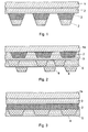
- Figures 1 to 6 possible structures for invisible are electrical conductive layers shown.
- 1 means a transparent one, 1a one colored and 1 b a metallized carrier substrate, which may already be can be printed, 2 a cover layer, 3 an electrically conductive layer, 4, 5 6 further functional and / or decorative, if any Layers and 7 a magnetic layer.
- the respective layers can be present on one side or on both sides of the carrier substrate.
- the substrate can be provided on one or both sides with protective lacquer layers, or be laminated or further refined, for example antistatic or scratch-resistant.
- the product is therefore possibly after appropriate packaging as a security element in data carriers, especially value documents such as ID cards, cards, banknotes or labels, seals and the like suitable, but also as packaging material in pharmaceutical Industry, for example in the form of blister films, for example for medicines, Covers or packaging to support compliance, or in the food industry as a food film for example Dairy products particularly suitable.
- Such products are also suitable for decorative applications or optical elements, for example in the Architecture and the like.
- They are particularly suitable substrates according to the invention for use in the electronics industry, for example as circuit boards, as RF antennas for example Transponders, SmartCards and the like, for displays, flexible circuits, medical facilities, electrode structures, as heatable foils, for example for windshields and the like.
- a covering layer consisting of 15% Al flakes in methyl ketone / ethyl acetate in a PVC / polyester dispersion is applied over the entire surface of a polyester film with a thickness of 75 ⁇ m. Then a layer of highly pigmented water-soluble paint is partially applied. A layer of an electrically conductive lacquer consisting of 15% graphite in a PVC / polyester dispersion is applied to this layer and then overprinted again with the described top layer. After drying, the highly pigmented paint and the electrically conductive layer thereon and the top layer are removed by treatment with water, the electrically conductive layer and the further top layer then remaining partially on the carrier substrate. The entire structure is then coated with a conventional protective polyurethane coating.
Abstract
Description
Die Erfindung betrifft Substrate mit unsichtbaren elektrisch leitfähigen Schichten.The invention relates to substrates with invisible electrically conductive Layers.
Bei der Herstellung von beschichteten Substraten werden üblicherweise
elektrisch leitfähige Farben oder Lacke zum Drucken elektrisch leitfähiger
Schichten verwendet. Den Farben oder Lacken werden dabei im allgemeinen
leitfähige Pigmente, beispielsweise Russ, Graphit, Silber und dergleichen
zugemischt. Allerdings sind die mit diesen Pigmenten versehenen Farben und
Lacke nach dem Aufbringen, insbesondere auch auf transparenten Substraten
deutlich sichtbar.
Bei verschiedenen Anwendungen ist es jedoch unerwünscht, dass diese
elektrisch leitfähigen Schichten sofort erkennbar sind. Dies trifft insbesondere
auf die Verwendung in Sicherheitsmerkmalen für Datenträger, Wertdokumente
und Produkte aller Art zu.In the production of coated substrates, electrically conductive inks or lacquers are usually used for printing electrically conductive layers. Conductive pigments, for example carbon black, graphite, silver and the like, are generally added to the paints or varnishes. However, the paints and varnishes provided with these pigments are clearly visible after application, especially on transparent substrates.
In various applications, however, it is undesirable for these electrically conductive layers to be immediately recognizable. This applies in particular to the use in security features for data carriers, value documents and products of all kinds.
Aus EP 0 426 801 sind beispielsweise Sicherheitselemente für
Sicherheitsdokumente bekannt, die Zeichen aufweisen, die im Auflicht
verborgen sind, im Durchlicht erkennbar werden und die außerdem elektrisch
leitend ausgeführt sind, wobei das elektrisch leitende Material vollflächig über
mindestens eine Oberfläche des Sicherheitselementes vorhanden ist und
zumindest in Teilbereichen transparent oder semitransparent ausgeführt ist und
über/oder unter den Zeichen angeordnet ist.
Dabei wird das transparente bzw. semitransparente Material entweder durch
eine Indium-Zinn-Oxidschicht oder durch Aufsputtem einer Metallschicht,
insbesondere einer Aluminiumschicht realisiert.From EP 0 426 801, for example, security elements for security documents are known which have characters which are hidden in incident light, are recognizable in transmitted light and which are also designed to be electrically conductive, the electrically conductive material being present over at least one surface of the security element and at least is made transparent or semi-transparent in partial areas and is arranged above / or below the characters.
The transparent or semi-transparent material is realized either by an indium tin oxide layer or by sputtering on a metal layer, in particular an aluminum layer.
Aufgabe der Erfindung ist daher die Bereitstellung von Substraten mit unsichtbaren elektrisch leitfähigen Schichten, die unsichtbar sowohl im Auf- als auch im Durchlicht sind und eine ausreichende Leitfähigkeit zur sicheren Identifizierung und die gewünschte Funktion auch bei Vorhandensein anderer funktioneller Schichten auf dem Substrat erlauben.The object of the invention is therefore to provide substrates with invisible electrically conductive layers that are invisible both in the up and down are also in transmitted light and have sufficient conductivity for safe Identification and the desired function even in the presence of others allow functional layers on the substrate.
Gegenstand der Erfindung sind daher Substrate mit mindestens einer elektrisch leitenden Schicht, dadurch gekennzeichnet, dass die elektrisch leitende Schicht unsichtbar eingebettet ist.The invention therefore relates to substrates with at least one electrical conductive layer, characterized in that the electrically conductive layer is invisibly embedded.
Als elektrisch leitfähige Schicht wird eine mit Ruß, Graphit oder Silber
pigmentierte Dispersion oder Lösung in Ethylenacrylatcopolymer.
Nitrocellulose, PVB, PA, Acrylat oder PVC oder deren Copolymeren verwendet.
Der Pigmentanteil kann bis zu 90 % betragen, gegebenenfalls kann der
Bindemittelanteil 20 - 70% betragen. Als Lösungsmittel kommen wässrige oder
nicht wässrige Lösungsmittel, beispielsweise Alkohole,
Alkohol/Wassermischungen, Methylethylketon, Ethylacetat und dergleichen in
Frage.A dispersion or solution pigmented with carbon black, graphite or silver in ethylene acrylate copolymer is used as the electrically conductive layer. Nitrocellulose, PVB, PA, acrylate or PVC or their copolymers are used.
The pigment content can be up to 90%, if necessary the binder content can be 20-70%. Suitable solvents are aqueous or non-aqueous solvents, for example alcohols, alcohol / water mixtures, methyl ethyl ketone, ethyl acetate and the like.
Diese elektrisch leitfähige Lackschicht kann partiell oder vollflächig aufgebracht werden.This electrically conductive lacquer layer can be applied partially or over the entire surface become.
Die elektrisch leitfähige Lackschicht kann erfindungsgemäß zwischen zwei
Schichten, die die pigmentierte Lackschicht vollständig abdecken, aufgebracht
werden.
Da Pigmente wie Ruß oder Graphit optisch sehr deutlich sichtbar sind, muss die
Zusammensetzung der Schichten, zwischen denen die leitfähige Schicht
gedruckt werden soll, vollständig deckend sein.
Die elektrisch leitende Schicht kann beispielsweise auch auf einem bereits
bedruckten, gefärbten oder metallisierten Trägersubstrat aufgebracht werden
und anschließend mit einer deckenden Lackschicht verborgen werden, oder
aber auch zwischen 2 deckenden Lackschichten aufgebracht werden.According to the invention, the electrically conductive lacquer layer can be applied between two layers which completely cover the pigmented lacquer layer.
Since pigments such as carbon black or graphite are very clearly visible, the composition of the layers between which the conductive layer is to be printed must be completely opaque.
The electrically conductive layer can, for example, also be applied to an already printed, colored or metallized carrier substrate and then hidden with an opaque lacquer layer, or else can be applied between 2 opaque lacquer layers.
Die deckende Lackschicht kann beispielsweise eine hochpigmentierte,
vorzugsweise mit Metallpigmenten oder Metallflakes oder eine Pigmente oder
Flakes von metallischen Verbindungen enthaltende Zusammensetzungen,
beispielsweise eine beispielsweise Silber oder Bronzen enthaltende
Zusammensetzung sein. Der Pigment- bzw. Flakesanteil kann 3 - 50%
betragen. Als Bindemittel kommen beispielsweise Ethylenacrylatcopolymer,
Nitrocellulose, PVB, PA, Acrylat oder PVC oder deren Copolymeren in Frage.
Die Farbschicht kann reaktiv, das heißt chemisch oder strahlungshärtend oder
nicht reaktiv sein.The covering lacquer layer can be, for example, a highly pigmented composition, preferably containing metal pigments or metal flakes or a pigment or flake of metallic compounds, for example a composition containing, for example, silver or bronzes. The pigment or flake content can be 3 - 50%. Examples of suitable binders are ethylene acrylate copolymer, nitrocellulose, PVB, PA, acrylate or PVC or their copolymers.
The color layer can be reactive, that is to say chemical or radiation-curing or non-reactive.
Gegebenenfalls kann das Trägermaterial vorher zur Verbesserung der Haftung mit einem Haftvermittler behandelt werden.If necessary, the carrier material can improve the adhesion beforehand be treated with an adhesion promoter.
Die Aufbringung der Schichten kann auf jede bekannte konventionelle Weise
erfolgen, beispielsweise durch Spin-Coating, Aufstreichen, Aufdampfen, durch
Drucken, (Tiefdruck, Flexodruck, Siebdruck, Digitaldruck und dergleichen)
durch Aufsprühen, Sputtem oder Walzenauftragstechniken.
Die elektrisch leitfähige Schicht und gegebenenfalls eine oder beide
umgebenden Lackschichten können sowohl vollflächig als auch partiell auf dem
Trägermaterial vorhanden sein.The layers can be applied in any known conventional manner, for example by spin coating, brushing, vapor deposition, by printing (gravure, flexographic, screen printing, digital printing and the like) by spraying, sputtering or roller application techniques.
The electrically conductive layer and optionally one or both surrounding lacquer layers can be present over the entire surface or partially on the carrier material.
Zur partiellen Aufbringung kann eine in einem Lösungsmittel lösliche Farbe oder ein löslicher Lack auf das Trägersubstrat oder etwaige bereits darauf befindliche Schichten aufgebracht werden. Anschließend wird die elektrisch leitfähige Lackschicht und/oder die Deckschicht auf diese Schicht aufgebracht, worauf die lösliche Farbe in den nicht beschichteten Bereichen mit Hilfe des geeigneten Lösungsmittels entfernt wird.For partial application, a solvent-soluble paint or a soluble varnish on the carrier substrate or any already on it existing layers are applied. Then the electrical conductive lacquer layer and / or the top layer applied to this layer, whereupon the soluble paint in the uncoated areas with the help of suitable solvent is removed.
Als Tägersubstrate kommen beispielsweise Trägerfolien, vorzugsweise flexible
transparente Kunststofffolien, beispielsweise aus Pl, PP, MOPP, PE, PPS,
PEEK, PEK, PEI, PAEK, LCP, PEN, PBT, PET, PA, PC, COC, POM, ABS, PVC
in Frage.
Die Trägerfolien weisen vorzugsweise eine Dicke von 5 - 700 µm, bevorzugt
8-200 µm, besonders bevorzugt 12 - 50 µm auf. Die Trägerfolien weisen
vorzugsweise eine Dicke von 5 - 700 µm, bevorzugt 8 - 200 µm, besonders
bevorzugt 12 - 50 µm auf.For example, carrier substrates, preferably flexible transparent plastic foils, for example made of PI, PP, MOPP, PE, PPS, PEEK, PEK, PEI, PAEK, LCP, PEN, PBT, PET, PA, PC, COC, POM, ABS, PVC, come as carrier substrates in question.
The carrier foils preferably have a thickness of 5-700 μm, preferably 8-200 μm, particularly preferably 12-50 μm. The carrier films preferably have a thickness of 5 to 700 μm, preferably 8 to 200 μm, particularly preferably 12 to 50 μm.
Femer können als Trägersubstrat auch Metallfolien, beispielsweise AI-, Cu-, Sn-, Ni-, Fe- oder Edelstahlfolien mit einer Dicke von 5 - 200 µm, vorzugsweise 10 bis 80 µm, besonders bevorzugt 20 - 50 µm dienen. Die Folien können auch oberflächenbehandelt, beschichtet oder kaschiert beispielsweise mit Kunststoffen oder lackiert sein.Furthermore, metal foils, for example Al, Cu, Sn, Ni, Fe or stainless steel foils with a thickness of 5 - 200 µm, serve preferably 10 to 80 microns, particularly preferably 20 - 50 microns. The Films can also be surface-treated, coated or laminated for example with plastics or painted.
Ferner können als Trägersubstrate auch Papier oder Verbunde mit Papier, beispielsweise Verbunde mit Kunststoffen mit einem Flächengewicht von 20 - 500 g/m2, vorzugsweise 40 - 200 g/m2. verwendet werden.Further, as carrier substrates also paper or composites with paper, for example, composites with plastics with a grammage 20-500 g / m 2, preferably 40-200 g / m 2. be used.
Femer können als Trägersubstrate Gewebe oder Vliese, wie Endlosfaservliese, Stapelfaservliese und dergleichen, die gegebenenfalls vemadelt oder kalandriert sein können, verwendet werden. Vorzugsweise bestehen solche Gewebe oder Vliese aus Kunststoffen, wie PP, PET, PA, PPS und dergleichen, es können aber auch Gewebe oder Vliese aus natürlichen, gegebenenfalls behandelten Fasern, wie Viskosefasem eingesetzt werden. Die eingesetzten Vliese oder Gewebe weisen ein Flächengewicht von etwa 20 g/m2 bis 500 g/m2 auf. Gegebenenfalls müssen die Vliese oder Gewebe oberflächenbehandelt werden.Woven or non-woven fabrics, such as continuous fiber non-woven fabrics, staple fiber non-woven fabrics and the like, which can optionally be needled or calendered, can also be used as carrier substrates. Such fabrics or nonwovens preferably consist of plastics, such as PP, PET, PA, PPS and the like, but fabrics or nonwovens made of natural, optionally treated fibers, such as viscose fibers, can also be used. The nonwovens or fabrics used have a weight per unit area of approximately 20 g / m 2 to 500 g / m 2 . If necessary, the nonwovens or fabrics must be surface-treated.
Das Trägersubstrat kann bereits funktionelle oder dekorative Schichten aufweisen, oder es können nach Aufbringen der leitfähigen Schicht weitere Schichten aufgebracht werden.The carrier substrate can already have functional or decorative layers have, or there may be more after application of the conductive layer Layers are applied.
Die Trägersubstrate können zusätzlich eine Lackschicht aufweisen, die unstrukturiert oder strukturiert, beispielsweise geprägt sein kann. Die Lackschicht kann beispielsweise eine releasefähige Transferlackschicht sein, sie kann durch Strahlung, beispielsweise UV-Strahlung vernetzt oder vernetzbar sein und kratzfest und/oder antistatisch ausgerüstet sein. Geeignet sind sowohl wässrige als auch feste Lacksysteme, insbesondere auch Lacksysteme auf Basis Nitrocellulose, Polyester-Acrylat oder Epoxyacrylat Kolophonium-, Acrylat-, Alkyd-, Melamin-, PVA-, PVC-, Isocyanat-, Urethansysteme, die konventionell und/oder reaktiv härtend und/oder strahlungshärtend) können.The carrier substrates can additionally have a lacquer layer that unstructured or structured, for example, can be shaped. The Lacquer layer can be, for example, a release-capable transfer lacquer layer, it can be cross-linked or by radiation, for example UV radiation be cross-linkable and scratch-resistant and / or antistatic. Suitable are both aqueous and solid coating systems, especially also Lacquer systems based on nitrocellulose, polyester acrylate or epoxy acrylate Rosin, acrylate, alkyd, melamine, PVA, PVC, isocyanate, Urethane systems that are conventional and / or reactive curing and / or radiation-curing).
Als Farb- bzw. Lackschichten können jeweils verschiedenste Zusammensetzungen verwendet werden. Die Zusammensetzung der einzelnen Schichten kann insbesondere nach deren Aufgabe variieren, also ob die einzelnen Schichten ausschließlich Dekorationszwecken dienen oder eine funktionelle Schicht sein sollen oder ob die Schicht sowohl eine Dekorationsals auch eine funktionelle Schicht sein soll.A wide variety of different layers of paint or varnish can be used Compositions are used. The composition of each Layers can vary in particular according to their task, i.e. whether the serve individual layers exclusively for decorative purposes or one functional layer or whether the layer is both a decorational should also be a functional layer.
Diese Schichten können pigmentiert oder nicht pigmentiert sein. Als Pigmente können alle bekannten Pigmente, wie beispielsweise Titandioxid, Zinksulfid, Kaolin, ITO, ATO, FTO, Aluminium, Chrom- und Siliciumoxide als auch farbige Pigmente verwendet werden. Dabei sind lösungsmittelhaltige Lacksysteme als auch System ohne Lösungsmittel verwendbar.These layers can be pigmented or unpigmented. As pigments all known pigments, such as titanium dioxide, zinc sulfide, Kaolin, ITO, ATO, FTO, aluminum, chromium and silicon oxides as well as colored ones Pigments are used. There are solvent-based paint systems as system can also be used without solvent.
Als Bindemittel kommen verschiedene natürliche oder synthetische Bindemittel in Frage.Various natural or synthetic binders come as binders in question.
Die weiteren funktionellen Schichten beispielsweise können bestimmte magnetische, chemische, physikalische und auch optische Eigenschaften aufweisen.The other functional layers, for example, can be certain magnetic, chemical, physical and also optical properties exhibit.
Zur Einstellung der magnetischen Eigenschaften können paramagnetische, diamagnetische und auch ferromagnetische Stoffe, wie Eisen, Nickel und Cobalt oder deren Verbindungen oder Salze (beispielsweise Oxide oder Sulfide) verwendet werden. To set the magnetic properties, paramagnetic, diamagnetic and also ferromagnetic materials such as iron, nickel and Cobalt or their compounds or salts (for example oxides or Sulfides) can be used.
Besonders geeignet zur Verwendung in Verbindung mit dem
erfindungsgemäßen elektrisch leitenden Schichtaufbau sind
Magnetpigmentfarben mit Pigmenten auf Basis von Fe-oxiden, Eisen, Nickel
Cobalt und deren Legierungen, Barium oder Cobalt-ferrite, hart- und weich
magnetische Eisen- und Stahlsorten in wässrigen bzw. lösungsmittelhaltigen
Dispersionen. Als Lösungsmittel kommen beispielsweise i-Propanol,
Ethylacetat, Methylethylketon, Methoxypropanol und deren Mischungen in
Frage.
Vorzugsweise sind die Pigmente in Acrylat- Polymerdispersionen mit einem
Molekulargewicht von 150.000 bis 300.000, in Acrylat-Urethan-Dispersionen,
Acrylat- Styrol oder PVC-haltigen Dispersionen oder in lösemittelhaltige
derartige Dispersionen eingebracht.Magnetic pigment paints with pigments based on Fe oxides, iron, nickel cobalt and their alloys, barium or cobalt ferrites, hard and soft magnetic iron and steel types in aqueous and / or steel types are particularly suitable for use in connection with the electrically conductive layer structure according to the invention. dispersions containing solvents. Examples of suitable solvents are i-propanol, ethyl acetate, methyl ethyl ketone, methoxypropanol and mixtures thereof.
The pigments are preferably incorporated in acrylate polymer dispersions with a molecular weight of 150,000 to 300,000, in acrylate urethane dispersions, acrylate styrene or PVC-containing dispersions or in solvent-containing dispersions of this type.
Besonders vorteilhaft kann diese Magnetpigmentfarbe auch mit den elektrisch leitfähigen Zusammensetzungen oder den Deckschicht-Zusammensetzungen vermischt werden.This magnetic pigment color can also be used particularly advantageously with the electrical conductive compositions or the top layer compositions be mixed.
Die Magnetpigmentfarbe kann aber auch partiell oder vollflächig neben und/oder unter und/oder über der leitfähigen Schicht aufgebracht werden.The magnetic pigment color can also partially or over the entire surface and / or are applied below and / or above the conductive layer.
Die optischen Eigenschaften einer oder mehrerer weiteren Schicht(en) lassen sich durch sichtbare Farbstoffe bzw. Pigmente, lumineszierende Farbstoffe bzw. Pigmente, die im sichtbaren, im UV-Bereich oder im IR-Bereich fluoreszieren bzw. phosphoreszieren, Effektpigmente, wie Flüssigkristalle, Perlglanz, Bronzen und/oder Multilayer-Farbumschlagpigmente und wärmeempfindliche Farben bzw. Pigmente beeinflussen. Diese sind in allen möglichen Kombinationen einsetzbar. Zusätzlich können auch phosphoreszierende Pigmente allein oder in Kombination mit anderen Farbstoffen und/oder Pigmenten eingesetzt werden.Leave the optical properties of one or more other layers visible dyes or pigments, luminescent dyes or pigments in the visible, in the UV range or in the IR range fluoresce or phosphoresce, effect pigments, such as liquid crystals, Pearlescent, bronzes and / or multilayer color change pigments and influence heat-sensitive colors or pigments. These are in all possible combinations can be used. In addition, too phosphorescent pigments alone or in combination with others Dyes and / or pigments are used.
Es können auch verschiedene Eigenschaften durch Zufügen verschiedener
oben genannter Zusätze kombiniert werden. So ist es möglich angefärbte
und/oder leitfähige Magnetpigmente zu verwenden. Dabei sind alle genannten
leitfähigen Zusätze verwendbar.
Speziell zum Anfärben von Magnetpigmenten lassen sich alle bekannten
löslichen und nicht löslichen Farbstoffe bzw. Pigmente verwenden. So kann
beispielsweise eine braune Magnetfarbe durch Zugabe von Metallen in ihrem
Farbton metallisch, z.B. silbrig eingestellt werden.Different properties can also be combined by adding different additives mentioned above. It is possible to use colored and / or conductive magnetic pigments. All of the conductive additives mentioned can be used.
All known soluble and non-soluble dyes or pigments can be used especially for coloring magnetic pigments. For example, a brown magnetic paint can be made metallic, for example silvery, by adding metals.
Zum Drucken löslicher Schichten insbesondere für die partielle Aufbringung funktioneller oder dekorativer Schichten kann die verwendete Farbe bzw. der verwendete Farblack in einem Lösungsmittel, vorzugsweise in Wasser löslich sein, es kann jedoch auch eine in jedem beliebigen Lösungsmittel, beispielsweise in Alkohol, Estern und dergleichen lösliche Farbe verwendet werden. Die Farbe bzw. der Farblack können übliche Zusammensetzungen auf Basis von natürlichen oder künstlichen Makromolekülen sein. Die Farbe kann pigmentiert oder nicht pigmentiert sein. Als Pigmente können alle bekannten Pigmente verwendet werden. Besonders geeignet sind TiO2, ZnS, Kaolin und dergleichen.For printing soluble layers, in particular for the partial application of functional or decorative layers, the color or the color lacquer used can be soluble in a solvent, preferably in water, but it can also be soluble in any solvent, for example in alcohol, esters and the like Color can be used. The color or the colored lacquer can be conventional compositions based on natural or artificial macromolecules. The color can be pigmented or unpigmented. All known pigments can be used as pigments. TiO 2 , ZnS, kaolin and the like are particularly suitable.
Bei Verwendung einer löslichen Farbschicht kann diese gegebenenfalls nach
Aufbringung einer weiteren Schicht im erfindungsgemäßen Verfahren durch ein
geeignetes Lösungsmittel, das auf die Zusammensetzung der Farbschicht
abgestimmt ist, entfernt werden, um Codierungen in Form von Zeichen
und/oder Mustern jeder möglichen Art herstellen zu können.
Anschließend wird die Farbschicht durch ein geeignetes Lösungsmittel, das auf
die Zusammensetzung der Farbschicht abgestimmt ist, entfernt. Bevorzugt ist
der Farbauftrag wasserlöslich. Gegebenenfalls kann die Ablösung durch
mechanische Einwirkung unterstützt werden.If a soluble color layer is used, this can optionally be removed after applying a further layer in the process according to the invention by means of a suitable solvent which is matched to the composition of the color layer, in order to be able to produce codes in the form of characters and / or patterns of any possible type.
The paint layer is then removed using a suitable solvent which is matched to the composition of the paint layer. The paint application is preferably water-soluble. If necessary, the detachment can be supported by mechanical action.
Um das Anlösen der abgedeckten Farbschicht weiter zu verbessern kann auch vollflächig oder passergenau eine dünne hochpigmentierte Farbschicht und/oder eine reine Pigmentschicht aufgebracht werden, wobei die Dicke dieser Schicht etwa 0,01 - 5 µm beträgt. To further improve the dissolving of the covered color layer, too a thin, highly pigmented layer of paint over the entire surface or in register and / or a pure pigment layer are applied, the thickness of this Layer is about 0.01 - 5 microns.
Durch das Ablösen des Farbauftrags mit den über dem Farbauftrag befindlichen Bereichen der funktionellen Schicht, wird das gewünschte Produkt erhalten.By peeling off the paint application with those above the paint application Areas of the functional layer, the desired product is obtained.
Femer können beispielsweise Isolatorschichten aufgebracht werden. Als
Isolatoren sind beispielsweise organische Substanzen und deren Derivate und
Verbindungen, beispielsweise Farb- und Lacksysteme, z.B. Epoxy-, Polyester-,
Kolophonium-, Acrylat-, Alkyd-, Melamin-, PVA-, PVC-, Isocyanat-,
Urethansysteme, die strahlungshärtend sein können, beispielsweise durch
Wärme- oder UV-Strahlung, geeignet.
Derartige Schichten können insbesondere bei der Herstellung von Multilayer-Aufbauten,
beispielsweise für Leiterplatten zwischen 2 oder mehren leitfähigen
Polymerschichten, die voneinander getrennt werden müssen, verwendet
werden.Insulator layers can also be applied, for example. Examples of insulators are organic substances and their derivatives and compounds, for example paint and lacquer systems, for example epoxy, polyester, rosin, acrylate, alkyd, melamine, PVA, PVC, isocyanate, urethane systems, which are radiation-curing can be suitable, for example by heat or UV radiation.
Layers of this type can be used in particular in the production of multilayer structures, for example for printed circuit boards between two or more conductive polymer layers which have to be separated from one another.
Diese Schichten können durch bekannte Verfahren, beispielsweise durch Bedampfen, Sputtern, Drucken (beispielsweise Tief-, Flexo-, Sieb-, Digitaldruck) und dergleichen) , Sprühen, Galvanisieren und dergleichen aufgebracht werden. Die Dicke der funktionellen Schicht beträgt 0,001 bis 50 µm, vorzugsweise 0,1 bis 20 µm.These layers can by known methods, for example by Steaming, sputtering, printing (e.g. gravure, flexo, screen, digital printing) and the like), spraying, electroplating and the like become. The thickness of the functional layer is 0.001 to 50 µm, preferably 0.1 to 20 µm.
Ferner können auf dem Trägersubstrat auch zusätzliche partielle oder
vollflächige metallische Schichten vorhanden sein oder anschließend
aufgebracht werden.
Diese Schicht besteht aus einem Metall, einer Metallverbindung oder einer
Legierung. Als Metallschicht sind Schichten aus Al, Cu, Fe, Ag, Au, Cr, Ni, Zn
und dergleichen geeignet. Als Metallverbindungen sind beispielsweise Oxide
oder Sulfide von Metallen, insbesondere TiO2, Cr-Oxide, ZnS, ITO, ATO, FTO,
ZnO, Al2O3 oder Siliciumoxide geeignet. Geeignete Legierungen sind
beispielsweise Cu-AI Legierungen, Cu-Zn Legierungen und dergleichen. Furthermore, additional partial or full-area metallic layers can also be present on the carrier substrate or subsequently applied.
This layer consists of a metal, a metal compound or an alloy. Layers of Al, Cu, Fe, Ag, Au, Cr, Ni, Zn and the like are suitable as the metal layer. Examples of suitable metal compounds are oxides or sulfides of metals, in particular TiO 2 , Cr oxides, ZnS, ITO, ATO, FTO, ZnO, Al 2 O 3 or silicon oxides. Suitable alloys are, for example, Cu-Al alloys, Cu-Zn alloys and the like.
Alle diese Schichten können sowohl vollflächig als auch partiell, passer- und registergenau, gegebenenfalls auch zumindest teilweise überlappend mit den bereits vorhandenen Schichten aufgebracht werden.All of these layers can be both full and partial, register and register-accurate, possibly also at least partially overlapping with the existing layers can be applied.
Werden hochpigmentierte System im Tiefdruckverfahren aufgebracht, so
entstehen auf der Folie, insbesondere in Abhängigkeit vom verwendeten Rakel,
unerwünschte Tonungsreste, d. h. es werden dünne Schichten außerhalb der
druckenden Bereiche auf die Folie appliziert. Dadurch kann die Haftung der
anschließend aufgebrachten Schichten verschlechtert werden.
Um die Entstehung derartiger Tonungsreste auf der Folie zu vermeiden, können
neben der Optimierung von Rakel und Zylinderrauhigkeit auch Systeme
eingesetzt werden, die diese dünnen Schichten bereits auf der
Zylinderoberfläche weitgehend abtrocknen und so eine Übertragung auf die
Folie verhindern.
So kann beispielsweise zwischen Rakel und Andruckwalze eine Blasleiste
situiert werden, mit mehreren über die gesamte Breite angeordneten Düsen.
Durch diese Düsen wird gefilterte Luft mit definierter Luftfeuchtigkeit,
gegebenenfalls beheizt oder gekühlt, mit gleicher Geschwindigkeit auf den
Druckzylinder gelenkt, wodurch die dünnen Schichten auf dem Zylinder
abtrocknen und nicht mehr auf das Trägersubstrat appliziert werden können.
Anstelle einer derartigen Blasleiste kann auch eine über die gesamte Breite
situierte IR-Trockeneinrichtung verwendet werden.
Entstandene Tonungsreste können aber auch beispielsweise durch Anwendung
eines Plasma- (Niederdruck- oder Atmosphärenplasma-), Corona- oder
Flammprozesses entfernt werden. Durch energiereiches Plasma,
beispielsweise Ar- oder Ar/O2-Plasma wird die Oberfläche von Tonungsresten
der Druckfarben gereinigt.If highly pigmented systems are applied using the gravure printing process, undesirable toning residues form on the film, in particular depending on the doctor blade used, ie thin layers are applied to the film outside the printing areas. As a result, the adhesion of the layers subsequently applied can be impaired.
In order to avoid the formation of such toning residues on the film, in addition to the optimization of the doctor blade and cylinder roughness, systems can also be used which largely dry these thin layers on the cylinder surface and thus prevent transmission to the film.
For example, a blow bar with several nozzles arranged over the entire width can be located between the doctor blade and the pressure roller. Through these nozzles, filtered air with defined air humidity, possibly heated or cooled, is directed onto the printing cylinder at the same speed, as a result of which the thin layers on the cylinder dry and can no longer be applied to the carrier substrate.
Instead of such a blow molding, an IR drying device situated over the entire width can also be used.
However, toning residues can also be removed, for example, by using a plasma (low-pressure or atmospheric plasma), corona or flame process. High-energy plasma, for example Ar or Ar / O 2 plasma, cleans the surface of toning residues in the printing inks.
Insbesondere bei der Aufbringung metallischer Schichten ist die gegebenenfalls zusätzliche Anwendung eines derartigen Prozesses vorteilhaft. This is particularly true when applying metallic layers additional application of such a process advantageous.
Gleichzeitig wird die dabei Oberfläche aktiviert. Dabei werden endständige polare Gruppen an der Oberfläche erzeugt. Dadurch wird die Haftung von Metallen und dergleichen an der Oberfläche verbessert.At the same time the surface is activated. This will be terminal polar groups are generated on the surface. This will limit the liability of Metals and the like improved on the surface.
Gegebenenfalls kann gleichzeitig mit der Anwendung der Plasma- bzw. Corona- oder Flammbehandlung eine dünne Metall- oder Metalloxidschicht als Haftvermittler, beispielsweise durch Sputtem oder Aufdampfen aufgebracht werden. Besonders geeignet sind dabei Cr, Al, Ag, Ti, Cu, TiO2, Si-Oxide oder Chromoxide. Diese Haftvermittlerschicht weist im allgemeinen eine Dicke von 0,1 nm - 5nm, vorzugsweise 0,2 nm - 2nm, besonders bevorzugt 0,2 bis 1 nm auf.If necessary, a thin metal or metal oxide layer can be applied as an adhesion promoter, for example by sputtering or vapor deposition, at the same time as the plasma, corona or flame treatment. Cr, Al, Ag, Ti, Cu, TiO 2 , Si oxides or chromium oxides are particularly suitable. This adhesion promoter layer generally has a thickness of 0.1 nm - 5 nm, preferably 0.2 nm - 2 nm, particularly preferably 0.2 to 1 nm.
Dadurch wird die Haftung einer weiteren partiell oder vollflächig aufgebrachten strukturierten funktionellen Schicht weiter verbessert. Das ist Voraussetzung für die Erzeugung von funktionellen Schichten mit hoher Präzision und guter Haftung.As a result, the liability of another is partially or fully applied structured functional layer further improved. That is a requirement for the production of functional layers with high precision and good Liability.
Es können zur Sicherstellung einer einwandfreien und sicheren Funktion oder Identifizierbarkeit auch unter erschwerten mechanischen Bedingungen, beispielsweise, wenn das Substrat im Gebrauch gedehnt oder auf irgendeine andere Weise mechanisch beansprucht wird, auch vorzugsweise passergenau elektrisch leitfähige Polymerschichten aufgebracht werden. Geeignet sind vorzugsweise Polymerschichten bestehend aus Polyanilin oder Polyethylendioxythiophen. Diese Schichten weisen eine ausgezeichnete mechanische Belastbarkeit auf und sind in der Lage, mechanische Beanspruchungen entstandene Risse in der erfindungsgemäß eingebetteten anorganischen elektrisch leitfähigen Schicht zu überbrücken und so eine sichere Funktion zu überbrücken. Dabei können die Polymerschichten in Form einer Dispersion oder Lösung des Polymeren oder in Form einer Lösung des Monomeren mit einem entsprechenden Katalysator oder Initiator durch in-situ-Polymerisation aufgebracht werden. Die Aufbringung kann über und/oder unter der konventionellen elektrisch leitfähigen Schicht erfolgen. It can be used to ensure proper and safe function or Identifiability even under difficult mechanical conditions, for example when the substrate is stretched or on any one in use is otherwise mechanically stressed, also preferably register-accurate electrically conductive polymer layers are applied. Are suitable preferably polymer layers consisting of polyaniline or Polyethylenedioxythiophene. These layers have an excellent mechanical resilience and are able to mechanical Cracks in the embedded according to the invention to bridge inorganic electrically conductive layer and so one bridge safe function. The polymer layers can be in shape a dispersion or solution of the polymer or in the form of a solution of the Monomers with an appropriate catalyst or initiator by in-situ polymerization be applied. The application can be over and / or under the conventional electrically conductive layer.
In den Figuren 1 bis 6 sind mögliche Aufbauten für unsichtbare elektrisch leitfähige Schichten dargestellt. Darin bedeuten 1 ein transparentes, 1a ein gefärbtes und 1 b ein metallisiertes Trägersubstrat, das gegebenenfalls bereits bedruckt sein kann, 2 eine Deckschicht, 3 eine elektrisch leitfähige Schicht, 4, 5 6 gegebenenfalls vorhandene weitere funktionelle und/oder dekorative Schichten und 7 eine magnetische Schicht.In Figures 1 to 6 possible structures for invisible are electrical conductive layers shown. 1 means a transparent one, 1a one colored and 1 b a metallized carrier substrate, which may already be can be printed, 2 a cover layer, 3 an electrically conductive layer, 4, 5 6 further functional and / or decorative, if any Layers and 7 a magnetic layer.
Die jeweiligen Schichten können auf einer Seite oder auf beiden Seiten des
Trägersubstrats vorhanden sein.
Gegebenenfalls kann das Substrat jeweils ein- oder beidseitig mit
Schutzlackschichten versehen sein, oder kaschiert sein oder weiter veredelt
sein, beispielsweise antistatisch oder kratzfest ausgerüstet sein.The respective layers can be present on one side or on both sides of the carrier substrate.
Optionally, the substrate can be provided on one or both sides with protective lacquer layers, or be laminated or further refined, for example antistatic or scratch-resistant.
Das Produkt ist gegebenenfalls nach entsprechender Konfektionierung daher als Sicherheitselement in Datenträgem, insbesondere Wertdokumenten wie Ausweisen, Karten, Banknoten oder Etiketten, Siegeln und dergleichen geeignet, aber auch als Verpackungsmaterial in der pharmazeutischen Industrie, beispielsweise in Form Blisterfolien, beispielsweise für Medikamente, Abdeckungen oder Verpackungen zur Unterstützung der Compliance, oder in der Lebensmittelindustrie als Lebensmittelfolie beispielsweise für Molkereiprodukte besonders geeignet. Ferner sind derartige Produkte auch für dekorative Anwendungen oder optische Elemente, beispielsweise in der Architektur und dergleichen geeignet. Besonders geeignet sind die erfindungsgemäßen Substrate zur Anwendung in der Elektronikindustrie, beispielsweise als Leiterplatten, als RF-Antennen beispielsweise für Transponder, SmartCards und dergleichen, für Displays, flexible Schaltungen, medizinische Einrichtungen, Elektrodenaufbauten, als heizbare Folien, beispielsweise für Windschutzscheiben und dergleichen . The product is therefore possibly after appropriate packaging as a security element in data carriers, especially value documents such as ID cards, cards, banknotes or labels, seals and the like suitable, but also as packaging material in pharmaceutical Industry, for example in the form of blister films, for example for medicines, Covers or packaging to support compliance, or in the food industry as a food film for example Dairy products particularly suitable. Such products are also suitable for decorative applications or optical elements, for example in the Architecture and the like. They are particularly suitable substrates according to the invention for use in the electronics industry, for example as circuit boards, as RF antennas for example Transponders, SmartCards and the like, for displays, flexible circuits, medical facilities, electrode structures, as heatable foils, for example for windshields and the like.
Auf einen Polyesterfolie einer Dicke von 75 µm wird eine Deckschicht
bestehend aus 15% AI-Flakes in Methylketon/Ethylacetat in einer
PVC/Polyesterdispersion vollflächig aufgebracht. Anschließend wird eine
Schicht hochpigmentierter wasserlöslicher Farbe partiell aufgebracht. Auf diese
Schicht wird eine Schicht eines elektrisch leitfähigen Lacks bestehend aus 15%
Graphit in einer PVC/Poiyesterdispersion aufgebracht und anschließend wieder
mit der beschriebenen Deckschicht überdruckt. Nach dem Trocknen wird die
hochpigmentierte Farbe und die darauf befindliche elektrisch leitfähige Schicht
und die Deckschicht durch Behandlung mit Wasser abgelöst, wobei die
elektrisch leitfähige Schicht und die weitere Deckschicht dann partiell auf dem
Trägersubstrat verbleiben.
Anschließend wird der gesamte Aufbau mit einer konventionellen
Polyurethanschutzlackschicht versehen.A covering layer consisting of 15% Al flakes in methyl ketone / ethyl acetate in a PVC / polyester dispersion is applied over the entire surface of a polyester film with a thickness of 75 μm. Then a layer of highly pigmented water-soluble paint is partially applied. A layer of an electrically conductive lacquer consisting of 15% graphite in a PVC / polyester dispersion is applied to this layer and then overprinted again with the described top layer. After drying, the highly pigmented paint and the electrically conductive layer thereon and the top layer are removed by treatment with water, the electrically conductive layer and the further top layer then remaining partially on the carrier substrate.
The entire structure is then coated with a conventional protective polyurethane coating.
Claims (8)
Applications Claiming Priority (2)
| Application Number | Priority Date | Filing Date | Title |
|---|---|---|---|
| AT6152002 | 2002-04-22 | ||
| AT0061502A AT412681B (en) | 2002-04-22 | 2002-04-22 | SUBSTRATES WITH INVISIBLE ELECTRICALLY CONDUCTIVE LAYERS |
Publications (2)
| Publication Number | Publication Date |
|---|---|
| EP1359792A1 true EP1359792A1 (en) | 2003-11-05 |
| EP1359792B1 EP1359792B1 (en) | 2005-12-21 |
Family
ID=28795533
Family Applications (1)
| Application Number | Title | Priority Date | Filing Date |
|---|---|---|---|
| EP03008531A Expired - Lifetime EP1359792B1 (en) | 2002-04-22 | 2003-04-12 | Substrate with non-visible electrically conducting layers |
Country Status (3)
| Country | Link |
|---|---|
| EP (1) | EP1359792B1 (en) |
| AT (2) | AT412681B (en) |
| DE (1) | DE50301963D1 (en) |
Cited By (8)
| Publication number | Priority date | Publication date | Assignee | Title |
|---|---|---|---|---|
| EP1559742A1 (en) * | 2004-01-15 | 2005-08-03 | Illochroma | Transparent plastic labels |
| WO2005106586A1 (en) * | 2004-04-29 | 2005-11-10 | Hueck Folien Gmbh & Co. Kg | Method for relief-printing highly conductive paths onto conducting substrates |
| WO2005115766A1 (en) * | 2004-05-24 | 2005-12-08 | Merck Patent Gmbh | Machine-readable security element for security products |
| EP1741564A1 (en) * | 2005-07-09 | 2007-01-10 | Hueck Folien GmbH & Co. KG | Tactile element used as security and authenticity feature |
| DE102010050823A1 (en) * | 2010-11-09 | 2012-05-10 | Giesecke & Devrient Gmbh | Security paper, method of making the same and security element |
| US10272469B2 (en) | 2015-05-27 | 2019-04-30 | Landa Labs (2012) Ltd. | Process for metallising a polymeric surface |
| US10583455B2 (en) | 2015-05-27 | 2020-03-10 | Actega Metal Print Gmbh | Coating apparatus |
| US11701684B2 (en) | 2015-05-27 | 2023-07-18 | Landa Labs (2012) Ltd. | Method for coating a surface with a transferable layer of thermoplastic particles and related apparatus |
Families Citing this family (1)
| Publication number | Priority date | Publication date | Assignee | Title |
|---|---|---|---|---|
| DE102016007732B4 (en) | 2016-06-23 | 2023-10-12 | Audi Ag | Galvanized plastic |
Citations (10)
| Publication number | Priority date | Publication date | Assignee | Title |
|---|---|---|---|---|
| WO1985004780A1 (en) * | 1984-04-06 | 1985-10-24 | American Telephone & Telegraph Company | Multilayer hybrid integrated circuit |
| US4601972A (en) * | 1984-04-06 | 1986-07-22 | At&T Technologies, Inc. | Photodefinable triazine based composition |
| EP0264617A1 (en) * | 1986-10-23 | 1988-04-27 | International Business Machines Corporation | Multilayer circuit board and method of manufacture therefor |
| EP0450701A1 (en) * | 1990-04-05 | 1991-10-09 | John L. Armitage & Co. | Conductive coating composition |
| EP0499986A2 (en) * | 1991-02-18 | 1992-08-26 | Hitachi, Ltd. | Multilayer wiring structure and method for forming multilayer construction |
| EP0666704A1 (en) * | 1994-02-04 | 1995-08-09 | Nippondenso Co., Ltd. | Flexible printed circuit board and manufacturing method therefor |
| US5536770A (en) * | 1993-10-16 | 1996-07-16 | Merck Patent Gesellschaft Mit Beschrankter Haftung | Conductive coating formulation |
| WO1999014994A1 (en) * | 1997-09-17 | 1999-03-25 | Telefonaktiebolaget Lm Ericsson | Multi-layer circuit board |
| EP0960912A1 (en) * | 1998-05-28 | 1999-12-01 | MERCK PATENT GmbH | Pigment mix |
| US6293008B1 (en) * | 1994-03-23 | 2001-09-25 | Dyconex Pantente Ag | Method for producing foil circuit boards |
Family Cites Families (5)
| Publication number | Priority date | Publication date | Assignee | Title |
|---|---|---|---|---|
| JPS61207472A (en) * | 1985-03-12 | 1986-09-13 | Achilles Corp | Electrically conductive transparent paint |
| DE3915638B4 (en) * | 1989-05-12 | 2006-06-08 | Giesecke & Devrient Gmbh | Security document with embedded security element with visually and machine-checkable tags and security element for a security document |
| JP3135412B2 (en) * | 1993-04-21 | 2001-02-13 | 松下電送システム株式会社 | Facsimile machine |
| TW505685B (en) * | 1997-09-05 | 2002-10-11 | Mitsubishi Materials Corp | Transparent conductive film and composition for forming same |
| JP2002083518A (en) * | 1999-11-25 | 2002-03-22 | Sumitomo Metal Mining Co Ltd | Transparent conductive substrate, its manufacturing method, display device using this transparent conductive substrate, coating solution for forming transparent conductive layer, and its manufacturing method |
-
2002
- 2002-04-22 AT AT0061502A patent/AT412681B/en not_active IP Right Cessation
-
2003
- 2003-04-12 EP EP03008531A patent/EP1359792B1/en not_active Expired - Lifetime
- 2003-04-12 DE DE50301963T patent/DE50301963D1/en not_active Expired - Lifetime
- 2003-04-12 AT AT03008531T patent/ATE313932T1/en active
Patent Citations (11)
| Publication number | Priority date | Publication date | Assignee | Title |
|---|---|---|---|---|
| WO1985004780A1 (en) * | 1984-04-06 | 1985-10-24 | American Telephone & Telegraph Company | Multilayer hybrid integrated circuit |
| US4601972A (en) * | 1984-04-06 | 1986-07-22 | At&T Technologies, Inc. | Photodefinable triazine based composition |
| EP0264617A1 (en) * | 1986-10-23 | 1988-04-27 | International Business Machines Corporation | Multilayer circuit board and method of manufacture therefor |
| EP0450701A1 (en) * | 1990-04-05 | 1991-10-09 | John L. Armitage & Co. | Conductive coating composition |
| EP0499986A2 (en) * | 1991-02-18 | 1992-08-26 | Hitachi, Ltd. | Multilayer wiring structure and method for forming multilayer construction |
| US5536770A (en) * | 1993-10-16 | 1996-07-16 | Merck Patent Gesellschaft Mit Beschrankter Haftung | Conductive coating formulation |
| EP0666704A1 (en) * | 1994-02-04 | 1995-08-09 | Nippondenso Co., Ltd. | Flexible printed circuit board and manufacturing method therefor |
| US6293008B1 (en) * | 1994-03-23 | 2001-09-25 | Dyconex Pantente Ag | Method for producing foil circuit boards |
| WO1999014994A1 (en) * | 1997-09-17 | 1999-03-25 | Telefonaktiebolaget Lm Ericsson | Multi-layer circuit board |
| US20010016980A1 (en) * | 1997-09-17 | 2001-08-30 | Lief Bergstedt | Multi-layer circuit board with supporting layers of different materials |
| EP0960912A1 (en) * | 1998-05-28 | 1999-12-01 | MERCK PATENT GmbH | Pigment mix |
Cited By (16)
| Publication number | Priority date | Publication date | Assignee | Title |
|---|---|---|---|---|
| EP1559742A1 (en) * | 2004-01-15 | 2005-08-03 | Illochroma | Transparent plastic labels |
| WO2005106586A1 (en) * | 2004-04-29 | 2005-11-10 | Hueck Folien Gmbh & Co. Kg | Method for relief-printing highly conductive paths onto conducting substrates |
| US8540812B2 (en) | 2004-05-24 | 2013-09-24 | Merck Patent Gmbh | Machine-readable security element for security products |
| WO2005115766A1 (en) * | 2004-05-24 | 2005-12-08 | Merck Patent Gmbh | Machine-readable security element for security products |
| CN100537266C (en) * | 2004-05-24 | 2009-09-09 | 默克专利股份有限公司 | Machine-readable security element for security products |
| US8039094B2 (en) | 2004-05-24 | 2011-10-18 | Merck Patent Gmbh | Machine-readable security element for security products |
| EP1741564A1 (en) * | 2005-07-09 | 2007-01-10 | Hueck Folien GmbH & Co. KG | Tactile element used as security and authenticity feature |
| EP2450196A3 (en) * | 2010-11-09 | 2016-11-02 | Giesecke & Devrient GmbH | Safety paper, method for manufacturing the same and safety element |
| DE102010050823A1 (en) * | 2010-11-09 | 2012-05-10 | Giesecke & Devrient Gmbh | Security paper, method of making the same and security element |
| US10272469B2 (en) | 2015-05-27 | 2019-04-30 | Landa Labs (2012) Ltd. | Process for metallising a polymeric surface |
| US10583455B2 (en) | 2015-05-27 | 2020-03-10 | Actega Metal Print Gmbh | Coating apparatus |
| US10751750B2 (en) | 2015-05-27 | 2020-08-25 | Actega Metal Print Gmbh | Coating apparatus with donor surface, application device, and surplus extraction system |
| US10906064B2 (en) | 2015-05-27 | 2021-02-02 | Actega Metal Print Gmbh | Printing system and method |
| US10981191B2 (en) | 2015-05-27 | 2021-04-20 | Actega Metal Print Gmbh | Metal printed constructions |
| US11679408B2 (en) | 2015-05-27 | 2023-06-20 | Actega Metal Print Gmbh | Printing system and method |
| US11701684B2 (en) | 2015-05-27 | 2023-07-18 | Landa Labs (2012) Ltd. | Method for coating a surface with a transferable layer of thermoplastic particles and related apparatus |
Also Published As
| Publication number | Publication date |
|---|---|
| ATA6152002A (en) | 2004-10-15 |
| EP1359792B1 (en) | 2005-12-21 |
| DE50301963D1 (en) | 2006-01-26 |
| AT412681B (en) | 2005-05-25 |
| ATE313932T1 (en) | 2006-01-15 |
Similar Documents
| Publication | Publication Date | Title |
|---|---|---|
| EP1291463B1 (en) | Process for producing a selectively metallized foil, and their products | |
| EP2851194B1 (en) | Safety element, in particular safety label | |
| DE10204281A1 (en) | A multicolored and/or multilayer printed material run with motives useful as e.g. safety strips, printed by digital process | |
| EP1356952B1 (en) | Coated supporting substrate with different optical and/or fluorescent characteristics at both sides | |
| EP1871616B1 (en) | Security element having a spatially resolved magnetic coding, method and device for producing the same and the use thereof | |
| EP1359792B1 (en) | Substrate with non-visible electrically conducting layers | |
| EP1636047A2 (en) | Security elements and chromophoric security features | |
| EP1584647B2 (en) | Sheet material with optical features | |
| EP1357226B1 (en) | Substrates with electrically conducting layers | |
| EP1386754B1 (en) | Data carrier and security element with visually detectable or machinally readable detection of manipulation | |
| EP1580297B1 (en) | Sheet material, especially for security elements | |
| AT504538B1 (en) | SUBSTRATES WITH ELECTRICALLY CONDUCTIVE LAYERS | |
| AT502160B1 (en) | SAFETY FOIL FOR SECURING DOCUMENTS | |
| EP1579394B1 (en) | Security element with combined machine-recognizable characteristics | |
| EP2006116B1 (en) | Safety element with colour-switching effect and visually imperceptible safety characteristics | |
| AT411977B (en) | DATA CARRIER OR CARRIER SUBSTRATE PROTECTIVE VARNISH RESISTANT TO PHYSICAL, MECHANICAL AND CHEMICAL EFFECTS | |
| WO2010130301A1 (en) | Safety feature and method for the production thereof | |
| EP1805033A1 (en) | Substrates comprising electroconductive layers | |
| EP1348576A2 (en) | UV laminated security thread | |
| EP1559540A1 (en) | Transfer film |
Legal Events
| Date | Code | Title | Description |
|---|---|---|---|
| PUAI | Public reference made under article 153(3) epc to a published international application that has entered the european phase |
Free format text: ORIGINAL CODE: 0009012 |
|
| AK | Designated contracting states |
Kind code of ref document: A1 Designated state(s): AT BE BG CH CY CZ DE DK EE ES FI FR GB GR HU IE IT LI LU MC NL PT RO SE SI SK TR |
|
| AX | Request for extension of the european patent |
Extension state: AL LT LV MK |
|
| 17P | Request for examination filed |
Effective date: 20040423 |
|
| AKX | Designation fees paid |
Designated state(s): AT BE BG CH CY CZ DE DK EE ES FI FR GB GR HU IE IT LI LU MC NL PT RO SE SI SK TR |
|
| 17Q | First examination report despatched |
Effective date: 20040824 |
|
| GRAP | Despatch of communication of intention to grant a patent |
Free format text: ORIGINAL CODE: EPIDOSNIGR1 |
|
| GRAS | Grant fee paid |
Free format text: ORIGINAL CODE: EPIDOSNIGR3 |
|
| GRAA | (expected) grant |
Free format text: ORIGINAL CODE: 0009210 |
|
| AK | Designated contracting states |
Kind code of ref document: B1 Designated state(s): AT BE BG CH CY CZ DE DK EE ES FI FR GB GR HU IE IT LI LU MC NL PT RO SE SI SK TR |
|
| PG25 | Lapsed in a contracting state [announced via postgrant information from national office to epo] |
Ref country code: IT Free format text: LAPSE BECAUSE OF FAILURE TO SUBMIT A TRANSLATION OF THE DESCRIPTION OR TO PAY THE FEE WITHIN THE PRESCRIBED TIME-LIMIT;WARNING: LAPSES OF ITALIAN PATENTS WITH EFFECTIVE DATE BEFORE 2007 MAY HAVE OCCURRED AT ANY TIME BEFORE 2007. THE CORRECT EFFECTIVE DATE MAY BE DIFFERENT FROM THE ONE RECORDED. Effective date: 20051221 Ref country code: GB Free format text: LAPSE BECAUSE OF FAILURE TO SUBMIT A TRANSLATION OF THE DESCRIPTION OR TO PAY THE FEE WITHIN THE PRESCRIBED TIME-LIMIT Effective date: 20051221 Ref country code: CZ Free format text: LAPSE BECAUSE OF FAILURE TO SUBMIT A TRANSLATION OF THE DESCRIPTION OR TO PAY THE FEE WITHIN THE PRESCRIBED TIME-LIMIT Effective date: 20051221 Ref country code: SI Free format text: LAPSE BECAUSE OF FAILURE TO SUBMIT A TRANSLATION OF THE DESCRIPTION OR TO PAY THE FEE WITHIN THE PRESCRIBED TIME-LIMIT Effective date: 20051221 Ref country code: IE Free format text: LAPSE BECAUSE OF FAILURE TO SUBMIT A TRANSLATION OF THE DESCRIPTION OR TO PAY THE FEE WITHIN THE PRESCRIBED TIME-LIMIT Effective date: 20051221 Ref country code: RO Free format text: LAPSE BECAUSE OF FAILURE TO SUBMIT A TRANSLATION OF THE DESCRIPTION OR TO PAY THE FEE WITHIN THE PRESCRIBED TIME-LIMIT Effective date: 20051221 Ref country code: FI Free format text: LAPSE BECAUSE OF FAILURE TO SUBMIT A TRANSLATION OF THE DESCRIPTION OR TO PAY THE FEE WITHIN THE PRESCRIBED TIME-LIMIT Effective date: 20051221 Ref country code: SK Free format text: LAPSE BECAUSE OF FAILURE TO SUBMIT A TRANSLATION OF THE DESCRIPTION OR TO PAY THE FEE WITHIN THE PRESCRIBED TIME-LIMIT Effective date: 20051221 Ref country code: NL Free format text: LAPSE BECAUSE OF FAILURE TO SUBMIT A TRANSLATION OF THE DESCRIPTION OR TO PAY THE FEE WITHIN THE PRESCRIBED TIME-LIMIT Effective date: 20051221 |
|
| REG | Reference to a national code |
Ref country code: GB Ref legal event code: FG4D Free format text: NOT ENGLISH |
|
| REG | Reference to a national code |
Ref country code: CH Ref legal event code: EP Ref country code: CH Ref legal event code: NV Representative=s name: BOVARD AG PATENTANWAELTE |
|
| REG | Reference to a national code |
Ref country code: IE Ref legal event code: FG4D Free format text: LANGUAGE OF EP DOCUMENT: GERMAN |
|
| REF | Corresponds to: |
Ref document number: 50301963 Country of ref document: DE Date of ref document: 20060126 Kind code of ref document: P |
|
| PG25 | Lapsed in a contracting state [announced via postgrant information from national office to epo] |
Ref country code: SE Free format text: LAPSE BECAUSE OF FAILURE TO SUBMIT A TRANSLATION OF THE DESCRIPTION OR TO PAY THE FEE WITHIN THE PRESCRIBED TIME-LIMIT Effective date: 20060321 Ref country code: GR Free format text: LAPSE BECAUSE OF FAILURE TO SUBMIT A TRANSLATION OF THE DESCRIPTION OR TO PAY THE FEE WITHIN THE PRESCRIBED TIME-LIMIT Effective date: 20060321 Ref country code: BG Free format text: LAPSE BECAUSE OF FAILURE TO SUBMIT A TRANSLATION OF THE DESCRIPTION OR TO PAY THE FEE WITHIN THE PRESCRIBED TIME-LIMIT Effective date: 20060321 Ref country code: DK Free format text: LAPSE BECAUSE OF FAILURE TO SUBMIT A TRANSLATION OF THE DESCRIPTION OR TO PAY THE FEE WITHIN THE PRESCRIBED TIME-LIMIT Effective date: 20060321 |
|
| PG25 | Lapsed in a contracting state [announced via postgrant information from national office to epo] |
Ref country code: ES Free format text: LAPSE BECAUSE OF FAILURE TO SUBMIT A TRANSLATION OF THE DESCRIPTION OR TO PAY THE FEE WITHIN THE PRESCRIBED TIME-LIMIT Effective date: 20060401 |
|
| PG25 | Lapsed in a contracting state [announced via postgrant information from national office to epo] |
Ref country code: BE Free format text: LAPSE BECAUSE OF NON-PAYMENT OF DUE FEES Effective date: 20060430 Ref country code: MC Free format text: LAPSE BECAUSE OF NON-PAYMENT OF DUE FEES Effective date: 20060430 |
|
| PG25 | Lapsed in a contracting state [announced via postgrant information from national office to epo] |
Ref country code: PT Free format text: LAPSE BECAUSE OF FAILURE TO SUBMIT A TRANSLATION OF THE DESCRIPTION OR TO PAY THE FEE WITHIN THE PRESCRIBED TIME-LIMIT Effective date: 20060522 |
|
| NLV1 | Nl: lapsed or annulled due to failure to fulfill the requirements of art. 29p and 29m of the patents act | ||
| PG25 | Lapsed in a contracting state [announced via postgrant information from national office to epo] |
Ref country code: HU Free format text: LAPSE BECAUSE OF FAILURE TO SUBMIT A TRANSLATION OF THE DESCRIPTION OR TO PAY THE FEE WITHIN THE PRESCRIBED TIME-LIMIT Effective date: 20060622 |
|
| GBV | Gb: ep patent (uk) treated as always having been void in accordance with gb section 77(7)/1977 [no translation filed] |
Effective date: 20051221 |
|
| REG | Reference to a national code |
Ref country code: IE Ref legal event code: FD4D |
|
| PLBE | No opposition filed within time limit |
Free format text: ORIGINAL CODE: 0009261 |
|
| STAA | Information on the status of an ep patent application or granted ep patent |
Free format text: STATUS: NO OPPOSITION FILED WITHIN TIME LIMIT |
|
| 26N | No opposition filed |
Effective date: 20060922 |
|
| EN | Fr: translation not filed | ||
| BERE | Be: lapsed |
Owner name: HUECK FOLIEN GMBH Effective date: 20060430 |
|
| PG25 | Lapsed in a contracting state [announced via postgrant information from national office to epo] |
Ref country code: FR Free format text: LAPSE BECAUSE OF FAILURE TO SUBMIT A TRANSLATION OF THE DESCRIPTION OR TO PAY THE FEE WITHIN THE PRESCRIBED TIME-LIMIT Effective date: 20070209 |
|
| PG25 | Lapsed in a contracting state [announced via postgrant information from national office to epo] |
Ref country code: EE Free format text: LAPSE BECAUSE OF FAILURE TO SUBMIT A TRANSLATION OF THE DESCRIPTION OR TO PAY THE FEE WITHIN THE PRESCRIBED TIME-LIMIT Effective date: 20051221 |
|
| PG25 | Lapsed in a contracting state [announced via postgrant information from national office to epo] |
Ref country code: LU Free format text: LAPSE BECAUSE OF NON-PAYMENT OF DUE FEES Effective date: 20060412 Ref country code: TR Free format text: LAPSE BECAUSE OF FAILURE TO SUBMIT A TRANSLATION OF THE DESCRIPTION OR TO PAY THE FEE WITHIN THE PRESCRIBED TIME-LIMIT Effective date: 20051221 |
|
| PG25 | Lapsed in a contracting state [announced via postgrant information from national office to epo] |
Ref country code: FR Free format text: LAPSE BECAUSE OF FAILURE TO SUBMIT A TRANSLATION OF THE DESCRIPTION OR TO PAY THE FEE WITHIN THE PRESCRIBED TIME-LIMIT Effective date: 20060430 |
|
| PG25 | Lapsed in a contracting state [announced via postgrant information from national office to epo] |
Ref country code: FR Free format text: LAPSE BECAUSE OF FAILURE TO SUBMIT A TRANSLATION OF THE DESCRIPTION OR TO PAY THE FEE WITHIN THE PRESCRIBED TIME-LIMIT Effective date: 20051221 Ref country code: CY Free format text: LAPSE BECAUSE OF FAILURE TO SUBMIT A TRANSLATION OF THE DESCRIPTION OR TO PAY THE FEE WITHIN THE PRESCRIBED TIME-LIMIT Effective date: 20051221 |
|
| REG | Reference to a national code |
Ref country code: CH Ref legal event code: PFA Owner name: HUECK FOLIEN GMBH Free format text: HUECK FOLIEN GMBH#GEWERBEPARK 30#4342 BAUMGARTENBERG (AT) -TRANSFER TO- HUECK FOLIEN GMBH#GEWERBEPARK 30#4342 BAUMGARTENBERG (AT) |
|
| PGFP | Annual fee paid to national office [announced via postgrant information from national office to epo] |
Ref country code: CH Payment date: 20160420 Year of fee payment: 14 Ref country code: DE Payment date: 20160421 Year of fee payment: 14 |
|
| PGFP | Annual fee paid to national office [announced via postgrant information from national office to epo] |
Ref country code: AT Payment date: 20160421 Year of fee payment: 14 |
|
| REG | Reference to a national code |
Ref country code: DE Ref legal event code: R119 Ref document number: 50301963 Country of ref document: DE |
|
| REG | Reference to a national code |
Ref country code: CH Ref legal event code: PL |
|
| REG | Reference to a national code |
Ref country code: AT Ref legal event code: MM01 Ref document number: 313932 Country of ref document: AT Kind code of ref document: T Effective date: 20170412 |
|
| PG25 | Lapsed in a contracting state [announced via postgrant information from national office to epo] |
Ref country code: DE Free format text: LAPSE BECAUSE OF NON-PAYMENT OF DUE FEES Effective date: 20171103 Ref country code: AT Free format text: LAPSE BECAUSE OF NON-PAYMENT OF DUE FEES Effective date: 20170412 |
|
| PG25 | Lapsed in a contracting state [announced via postgrant information from national office to epo] |
Ref country code: CH Free format text: LAPSE BECAUSE OF NON-PAYMENT OF DUE FEES Effective date: 20170430 Ref country code: LI Free format text: LAPSE BECAUSE OF NON-PAYMENT OF DUE FEES Effective date: 20170430 |