EP1357661A2 - Circuit design for variable application of an input voltage to a circuit - Google Patents
Circuit design for variable application of an input voltage to a circuit Download PDFInfo
- Publication number
- EP1357661A2 EP1357661A2 EP03252619A EP03252619A EP1357661A2 EP 1357661 A2 EP1357661 A2 EP 1357661A2 EP 03252619 A EP03252619 A EP 03252619A EP 03252619 A EP03252619 A EP 03252619A EP 1357661 A2 EP1357661 A2 EP 1357661A2
- Authority
- EP
- European Patent Office
- Prior art keywords
- circuit
- terminals
- voltage
- circuit design
- design according
- Prior art date
- Legal status (The legal status is an assumption and is not a legal conclusion. Google has not performed a legal analysis and makes no representation as to the accuracy of the status listed.)
- Granted
Links
Images
Classifications
-
- H—ELECTRICITY
- H02—GENERATION; CONVERSION OR DISTRIBUTION OF ELECTRIC POWER
- H02M—APPARATUS FOR CONVERSION BETWEEN AC AND AC, BETWEEN AC AND DC, OR BETWEEN DC AND DC, AND FOR USE WITH MAINS OR SIMILAR POWER SUPPLY SYSTEMS; CONVERSION OF DC OR AC INPUT POWER INTO SURGE OUTPUT POWER; CONTROL OR REGULATION THEREOF
- H02M1/00—Details of apparatus for conversion
- H02M1/10—Arrangements incorporating converting means for enabling loads to be operated at will from different kinds of power supplies, e.g. from AC or DC
Definitions
- the present invention relates to a circuit design by means of which an input voltage can be applied in a variable manner to a circuit which comprises two or more circuit components.
- the circuit is, in particular, a circuit in trains, by means of which different train busbar voltages can be converted to an intermediate-circuit voltage.
- the train busbar voltage is in this case converted by voltage conversion circuits to a so-called intermediate-circuit voltage, for example to a DC voltage of 670 Volts, which, possibly after further conversion, is then used to supply various devices in the train power supply system.
- the problem is that, if it is necessary to rewire the cables which carry the input voltage, in this case by way of example the train busbar voltage, to the circuit components, for example to the high-voltage converters, in this case for the different connections of circuit components, when the input voltage has to be connected to the circuit components in a different way because the input voltage is different, this represents a highly labour-intensive, tedious and thus expensive procedure.
- the object of the present invention is therefore to specify a circuit design by means of which an input voltage can be applied in an easily variable manner to a circuit which comprises different circuit components.
- the circuit design should in this case be suitable in particular for use in trains for the conversion of a variable train busbar voltage to a constant intermediate-circuit voltage using voltage conversion elements, such as high-voltage converters.
- the circuit design according to the invention has two or more terminals.
- the input voltage is in this case connected to two of these terminals.
- Two further terminals are in this case also connected to the input of a circuit component which the input voltage is intended to supply.
- two terminals are in each case connected by means of bridging elements in an appropriate manner.
- the bridging elements may, for example, be wire links, which can be plugged onto the terminals, or screwed to them, in various ways, or solid lugs which can be connected to the terminals in various ways, or else switchable elements, in particular contactors.
- the terminals are at the same distance from one another since bridging elements that are the same as one another, that is to say bridging elements with the same external dimensions for the connections, can then be used for bridging or connection of the terminals.
- these terminals may be arranged in different ways. For example, it is possible for them to be arranged in the form of a row, in the form of a rectangle, in the form of a parallelogram or in the form of a triangle. In this case, the terminals should advantageously be connected such that the terminals to be bridged are adjacent to one another, so that there are no crossovers in the bridges.
- the circuit design according to the invention can be used in a general form for variable application of an input voltage to different circuit components, and it is particularly suitable for use for the conversion of a variable train busbar voltage to a constant intermediate-circuit voltage, using voltage conversion elements such as high-voltage converters.
- circuit design according to the invention will be described in more detail in the following text with reference to an embodiment for conversion of a variable train busbar voltage to a constant intermediate-circuit voltage using voltage conversion elements as shown in the figures in the drawing.
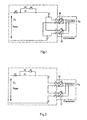
- Figure 1 shows, schematically, a conversion circuit for the conversion of a train busbar voltage U s to an intermediate-circuit voltage U z .
- Two voltage conversion elements for example high-voltage converters 10 and 12, are in this case provided for the conversion process.
- the circuit has six terminals 1, 2, 3, 4, 5 and 6, which are annotated by hollow circles.
- the terminals 1 and 2 are in this case connected to the train busbar voltage via input elements such as fuses or resistors, which may be required here but are not of any further interest for the invention.
- the terminals 3 and 4 are connected to the input of the first voltage conversion element 10, and the terminals 5 and 6 are connected to the input of the second voltage conversion element 12.
- the outputs of the voltage conversion elements 10 and 12 are connected in parallel by means of two output lines to the terminals at which the intermediate-circuit voltage U z which can be tapped off is produced.
- Figure 1 shows the voltage conversion elements connected in parallel.
- the circuit shown in Figure 2 corresponds to the circuit shown in Figure 1, but in this case with the two voltage conversion elements 10 and 12 being arranged in the form of a series circuit.
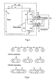
- the circuit shown in Figure 3 represents a combination of the circuits shown in Figure 1 and Figure 2.
- the two voltage conversion elements 10 and 12 can be arranged either in the form of a parallel circuit or in the form of a series circuit.
- Five switches K11, K12, K13, K14 and K15 are provided for this purpose and may, by way of example, be contactors. When the switches K11, K12, K13 and K14 are closed, then the voltage conversion elements 10 and 12 are connected in parallel, and when the switches K12, K13 and K15 are closed, then the voltage conversion elements are connected in series.
- Figure 4 shows an arrangement of the terminals 1, 2, 3, 4, 5 and 6 in the form of a row.
- the terminals are advantageously all at the same distance a apart from one another.
- the terminals in the uppermost row are all shown without any connection. This is intended to represent the situation in which switches are provided between the terminals, as is shown in Figure 3, so that the terminals can be connected to one another in different ways by closing the switches.
- the centre row represents the connection of the terminals 3 and 1, of the terminals 5 and 4 and of the terminals 2 and 6 by means of in each case one bridging element 14. Connecting the terminals in this way results in the voltage conversion elements 10 and 12 being connected in series, as is shown in Figure 2.
- the lower row represents the connection of the terminals 3 and 1, 1 and 5 and of the terminals 4 and 2, 2 and 6 by means of in each case one bridging element 14. Connecting the terminals in this way results in the voltage conversion elements 10 and 12 being connected in parallel, as is illustrated in Figure 1.
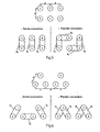
- Figure 5 shows an arrangement of the terminals 1, 2, 3, 4, 5 and 6 in the form of a rectangle.
- the terminals are once again advantageously all at the same distance a apart from one another here.
- the terminals 1, 3, 4 and 5 are thus likewise arranged in the same way as the terminals 2, 4, 5 and 6 in the form of a square.
- the terminals in the uppermost rectangle are all shown without any connection. Once again, this is intended to represent the situation in which switches are provided between the terminals, as is shown in Figure 3, such that the terminals can be connected to one another in different ways by closing the switches.
- the left lower rectangle shows the connection of the terminals 3 and 1, of the terminals 5 and 4 and of the terminals 2 and 6 by means of in each case one bridging element 14.
- Figure 6 shows an arrangement of the terminals 1, 2, 3, 4, 5 and 6 in the form of a triangle (which is open at the top). As can easily be seen, the terminals are also once again advantageously all at the same distance apart from one another here. In the same way as the terminals 2, 4 and 6, the terminals 1, 3 and 5 are in this case arranged in the form of an equilateral triangle. The terminals in the uppermost triangle are all shown without any connection. Once again, this is intended to represent the situation in which switches are provided between the terminals, as is shown in Figure 3, so that the terminals can be connected to one another in different ways by closing the switches. In the left lower triangle, the terminals 3 and 1, the terminals 5 and 4 and of the terminals 2 and 6 are each connected by means of a bridging element 14.
- terminals it is also feasible, although this is not shown here, for the terminals to be arranged in the form of a parallelogram. The chosen arrangement of the terminals will depend on the specific space and connection conditions.
Landscapes
- Engineering & Computer Science (AREA)
- Power Engineering (AREA)
- Amplifiers (AREA)
- Inverter Devices (AREA)
- Measurement Of Current Or Voltage (AREA)
- Power Conversion In General (AREA)
- Analogue/Digital Conversion (AREA)
- Logic Circuits (AREA)
- Networks Using Active Elements (AREA)
- Electric Propulsion And Braking For Vehicles (AREA)
Abstract
Description
- a
- Distance between terminals
- 1, 2, 3, 4, 5, 6
- Terminals
- 10
- First voltage conversion element (circuit component)
- 12
- Second voltage conversion element (circuit component)
- 14
- Bridging element
- K11, K12, K13, K14, K15
- Switches
- Us
- Busbar voltage (input voltage)
- Uz
- Intermediate-circuit voltage (output voltage)
Claims (13)
- Circuit design for variable application of an input voltage (Us) to a circuit which comprises at least two circuit components (10, 12) which each have two input connections, characterized in that the circuit design has two terminals (1, 2) for the input voltage (Us) and in each case two terminals (3, 4 and 5, 6) for the input connections of the at least two circuit components (10, 12), and in that two terminals with bridging elements (14) are in each case connected to one another in a desired manner for variable application of the input voltage (Us).
- Circuit design according to Claim 1, characterized in that the terminals (1, 2, 3, 4, 5, 6) are all the same distance (a) apart from one another.
- Circuit design according to Claim 1 or 2, characterized in that the terminals (1, 2, 3, 4, 5, 6) are arranged in a row.
- Circuit design according to Claim 1 or 2, characterized in that the terminals (1, 2, 3, 4, 5, 6) are arranged in the form of a rectangle.
- Circuit design according to Claim 1 or 2, characterized in that the terminals (1, 2, 3, 4, 5, 6) are arranged in the form of a parallelogram.
- Circuit design according to Claim 1 or 2, characterized in that the terminals (1, 2, 3, 4, 5, 6) are arranged in the form of a triangle.
- Circuit design according to one of the preceding claims, characterized in that the bridging of in each case two terminals by means of a bridging element (14) on the one hand provides a connection between the at least two circuit components (10, 12) and the input voltage (Us) in the form of a series circuit, and on the other hand provides a connection between the two circuit components (10, 12) and the input voltage (Us) in the form of a parallel circuit.
- Circuit design according to one of the preceding claims, characterized in that the bridging elements (14) are wire links which can be pushed or screwed in.
- Circuit design according to one of the preceding claims, characterized in that the bridging elements are solid lugs (14) which can be pushed or screwed in.
- Circuit design according to one of Claims 1 to 7, characterized in that the bridging elements (14) are switchable elements (K11, K12, K13, K14, K15), in particular contactors.
- Circuit design according to one of the preceding claims, characterized in that the circuit components are voltage conversion elements (10, 12).
- Circuit design according to Claim 11, characterized in that the voltage conversion elements (10, 12) are high-voltage converters.
- Circuit design according to Claim 12, characterized in that the circuit is a circuit in trains, for the conversion of different train busbar voltages (Us) to an intermediate-circuit voltage (Uz) which, possibly after further conversion, is used for supplying various devices in a train power supply system.
Applications Claiming Priority (2)
| Application Number | Priority Date | Filing Date | Title |
|---|---|---|---|
| DE10219645 | 2002-04-26 | ||
| DE10219645A DE10219645A1 (en) | 2002-05-02 | 2002-05-02 | Setup for changeable application of an input voltage to a circuit |
Publications (4)
| Publication Number | Publication Date |
|---|---|
| EP1357661A2 true EP1357661A2 (en) | 2003-10-29 |
| EP1357661A3 EP1357661A3 (en) | 2005-07-13 |
| EP1357661B1 EP1357661B1 (en) | 2008-03-26 |
| EP1357661B8 EP1357661B8 (en) | 2008-06-11 |
Family
ID=28685333
Family Applications (1)
| Application Number | Title | Priority Date | Filing Date |
|---|---|---|---|
| EP03252619A Expired - Lifetime EP1357661B8 (en) | 2002-05-02 | 2003-04-25 | Circuit design for variable application of an input voltage to a circuit |
Country Status (3)
| Country | Link |
|---|---|
| EP (1) | EP1357661B8 (en) |
| AT (1) | ATE390750T1 (en) |
| DE (2) | DE10219645A1 (en) |
Family Cites Families (29)
| Publication number | Priority date | Publication date | Assignee | Title |
|---|---|---|---|---|
| CH83200A (en) * | 1919-02-26 | 1920-04-16 | Jonas Julius Ing Dipl | Switching device consisting of plug and mating plug for power consumers to be connected to electrical lines |
| NL30658C (en) * | 1929-01-07 | |||
| US3012206A (en) * | 1958-06-10 | 1961-12-05 | Sunair Electronics Inc | Electronic inverters |
| DE1116917B (en) * | 1958-09-27 | 1961-11-09 | Erich Zillmer | Mains voltage switch for electrically operated projector |
| US3231767A (en) * | 1962-07-18 | 1966-01-25 | Smith Corp A O | Circuit selection switch |
| DE1413609A1 (en) * | 1962-09-01 | 1969-10-02 | Siemens Ag | Equipment for the supply of auxiliary services on multi-system locomotives |
| FR1407491A (en) * | 1963-09-12 | 1965-07-30 | Licentia Gmbh | Electric railcar with lighted direct current traction motors through bridge assemblies with rectifiers |
| GB1108005A (en) * | 1965-10-26 | 1968-03-27 | Amp Inc | Metal strip for connecting electrical posts |
| DE1945678B2 (en) * | 1969-09-10 | 1976-02-19 | Unomat Gmbh & Co Kg, 7411 Reutlingen | Voltage selector switch for charging circuits - consists of moveable plate with offset contact areas to give two different voltages |
| US3846695A (en) * | 1973-05-07 | 1974-11-05 | Honeywell Inf Systems | Series-parallel dual switching regulator for use with a variety of line voltages |
| US3983428A (en) * | 1974-06-10 | 1976-09-28 | Emerson Electrical Co. | Interchangeable connector means for electric motor operation on either of two supply voltages |
| DE2504120A1 (en) * | 1975-01-31 | 1976-08-05 | Paul Boswinkel | Socket for alternative full or dimmed lighting - has six-contact sleeves to give series or parallel connection |
| US4178578A (en) * | 1977-10-11 | 1979-12-11 | Gary Lester Hall | Pest control apparatus |
| US4408154A (en) * | 1981-09-02 | 1983-10-04 | General Electric Company | Dual voltage power supply with input filter |
| JPS59162774A (en) * | 1983-03-04 | 1984-09-13 | Fujitsu Ltd | Switching method of ac input voltage |
| DE3615851A1 (en) * | 1986-05-10 | 1987-11-12 | Oplaender Wilo Werk Gmbh | Single-phase motor |
| DE3817652A1 (en) * | 1988-05-25 | 1989-12-07 | Asea Brown Boveri | Electrically operated tractive unit with at least two drive systems |
| US5017818A (en) * | 1989-06-02 | 1991-05-21 | Emerson Electric Co. | Voltage change and motor rotation reversal device |
| DE3935414A1 (en) * | 1989-10-24 | 1991-04-25 | Manfred Herrmann | Series or parallel LV source connector for consumer - has insulated carrier for at least six contact sockets |
| JPH0479768A (en) * | 1990-07-18 | 1992-03-13 | Fuji Electric Co Ltd | Different voltage input apparatus |
| JPH07115182B2 (en) * | 1991-10-07 | 1995-12-13 | 株式会社三社電機製作所 | Arc welder |
| FR2688635B1 (en) * | 1992-03-13 | 1994-05-27 | Leroy Somer Moteurs | PLATE WITH TWELVE TERMINALS FOR THE CONNECTION OF AN ASYNCHRONOUS THREE-PHASE ELECTRIC MOTOR WITH SIX WINDINGS, AND MOTOR COMPRISING SUCH A PLATE. |
| EP0676854B1 (en) * | 1994-04-08 | 2001-12-12 | Vlt Corporation | Efficient power conversion |
| DE19639163A1 (en) * | 1996-09-24 | 1998-04-02 | Veba Kraftwerke Ruhr | Device for adapting a consumer to the feeding mains voltage |
| US6048219A (en) * | 1998-06-23 | 2000-04-11 | Illinois Tool Works Inc. | Voltage selection electrical connector |
| AT406625B (en) * | 1998-11-12 | 2000-07-25 | Fronius Schweissmasch | VOLTAGE SWITCHING DEVICE |
| US6370047B2 (en) * | 2000-03-10 | 2002-04-09 | Power-One, Inc. | Dual input range power supply using two series or parallel connected converter sections with automatic power balancing |
| GB0019925D0 (en) * | 2000-08-15 | 2000-09-27 | Linn Prod Ltd | Multipe configuration loudspeaker terminals |
| US6269015B1 (en) * | 2000-11-08 | 2001-07-31 | Sansha Electric Manufacturing Company, Limited | Power supply apparatus for ARC-utilizing apparatuses |
-
2002
- 2002-05-02 DE DE10219645A patent/DE10219645A1/en not_active Ceased
-
2003
- 2003-04-25 AT AT03252619T patent/ATE390750T1/en active
- 2003-04-25 DE DE60319906T patent/DE60319906T2/en not_active Expired - Lifetime
- 2003-04-25 EP EP03252619A patent/EP1357661B8/en not_active Expired - Lifetime
Also Published As
| Publication number | Publication date |
|---|---|
| ATE390750T1 (en) | 2008-04-15 |
| EP1357661B1 (en) | 2008-03-26 |
| DE60319906T2 (en) | 2009-04-16 |
| DE10219645A1 (en) | 2003-11-20 |
| EP1357661B8 (en) | 2008-06-11 |
| DE60319906D1 (en) | 2008-05-08 |
| EP1357661A3 (en) | 2005-07-13 |
Similar Documents
| Publication | Publication Date | Title |
|---|---|---|
| EP3114763B1 (en) | Multilevel converter | |
| DK2086102T3 (en) | Alternators for converting an electric DC voltage to an alternating current or alternating voltage | |
| CN114364567B (en) | Vehicle charging circuit and vehicle-mounted network with same | |
| JP5497234B1 (en) | Load testing equipment | |
| CN104081649B (en) | The AC/DC multi-unit power transducer that two-terminal HVDC is connected | |
| CN110999066B (en) | voltage source converter | |
| EP2822164B1 (en) | Multi-level medium-voltage inverter | |
| HUT68302A (en) | Inverter, especially a 3-point inverter | |
| MX2007014966A (en) | Micro-electromechanical system based switching module serially stackable with other such modules to meet a voltage rating. | |
| JP6648535B2 (en) | DC power supply | |
| DE10344563A1 (en) | DC electrical system | |
| US20150102671A1 (en) | Direct current power transmission system | |
| KR20160040378A (en) | Dab convertor with multi-phase structure | |
| CN103384120A (en) | Power supply device | |
| EP1357661B1 (en) | Circuit design for variable application of an input voltage to a circuit | |
| CN108781040A (en) | Modular multistage converter | |
| JPH1189247A (en) | Power converter | |
| JPH09274904A (en) | Battery array wiring method | |
| CN106797182B (en) | Device for connecting railway power supply of railway lines to a three-phase power supply network | |
| US20020126511A1 (en) | Energy converter | |
| US11395407B2 (en) | Intermediate circuit arrangement and inverter | |
| JP2003174782A (en) | Power converter | |
| EP3017996A1 (en) | Vehicle with a power distribution system and power distribution system | |
| CN205356163U (en) | A module for light , cladon and power transfer ware for power transfer ware | |
| JPH11308881A (en) | Overvoltage suppression device |
Legal Events
| Date | Code | Title | Description |
|---|---|---|---|
| PUAI | Public reference made under article 153(3) epc to a published international application that has entered the european phase |
Free format text: ORIGINAL CODE: 0009012 |
|
| AK | Designated contracting states |
Kind code of ref document: A2 Designated state(s): AT BE BG CH CY CZ DE DK EE ES FI FR GB GR HU IE IT LI LU MC NL PT RO SE SI SK TR |
|
| AX | Request for extension of the european patent |
Extension state: AL LT LV MK |
|
| PUAL | Search report despatched |
Free format text: ORIGINAL CODE: 0009013 |
|
| AK | Designated contracting states |
Kind code of ref document: A3 Designated state(s): AT BE BG CH CY CZ DE DK EE ES FI FR GB GR HU IE IT LI LU MC NL PT RO SE SI SK TR |
|
| AX | Request for extension of the european patent |
Extension state: AL LT LV MK |
|
| 17P | Request for examination filed |
Effective date: 20060111 |
|
| AKX | Designation fees paid |
Designated state(s): AT BE BG CH CY CZ DE DK EE ES FI FR GB GR HU IE IT LI LU MC NL PT RO SE SI SK TR |
|
| GRAP | Despatch of communication of intention to grant a patent |
Free format text: ORIGINAL CODE: EPIDOSNIGR1 |
|
| GRAS | Grant fee paid |
Free format text: ORIGINAL CODE: EPIDOSNIGR3 |
|
| GRAA | (expected) grant |
Free format text: ORIGINAL CODE: 0009210 |
|
| AK | Designated contracting states |
Kind code of ref document: B1 Designated state(s): AT BE BG CH CY CZ DE DK EE ES FI FR GB GR HU IE IT LI LU MC NL PT RO SE SI SK TR |
|
| REG | Reference to a national code |
Ref country code: GB Ref legal event code: FG4D |
|
| RAP2 | Party data changed (patent owner data changed or rights of a patent transferred) |
Owner name: BOMBARDIER TRANSPORTATION GMBH |
|
| REG | Reference to a national code |
Ref country code: IE Ref legal event code: FG4D Ref country code: CH Ref legal event code: EP |
|
| REF | Corresponds to: |
Ref document number: 60319906 Country of ref document: DE Date of ref document: 20080508 Kind code of ref document: P |
|
| NLT2 | Nl: modifications (of names), taken from the european patent patent bulletin |
Owner name: BOMBARDIER TRANSPORTATION GMBH Effective date: 20080416 |
|
| PG25 | Lapsed in a contracting state [announced via postgrant information from national office to epo] |
Ref country code: FI Free format text: LAPSE BECAUSE OF FAILURE TO SUBMIT A TRANSLATION OF THE DESCRIPTION OR TO PAY THE FEE WITHIN THE PRESCRIBED TIME-LIMIT Effective date: 20080326 |
|
| REG | Reference to a national code |
Ref country code: CH Ref legal event code: NV Representative=s name: ABREMA AGENCE BREVET ET MARQUES, GANGUILLET |
|
| PG25 | Lapsed in a contracting state [announced via postgrant information from national office to epo] |
Ref country code: SI Free format text: LAPSE BECAUSE OF FAILURE TO SUBMIT A TRANSLATION OF THE DESCRIPTION OR TO PAY THE FEE WITHIN THE PRESCRIBED TIME-LIMIT Effective date: 20080326 |
|
| ET | Fr: translation filed | ||
| PG25 | Lapsed in a contracting state [announced via postgrant information from national office to epo] |
Ref country code: ES Free format text: LAPSE BECAUSE OF FAILURE TO SUBMIT A TRANSLATION OF THE DESCRIPTION OR TO PAY THE FEE WITHIN THE PRESCRIBED TIME-LIMIT Effective date: 20080707 Ref country code: PT Free format text: LAPSE BECAUSE OF FAILURE TO SUBMIT A TRANSLATION OF THE DESCRIPTION OR TO PAY THE FEE WITHIN THE PRESCRIBED TIME-LIMIT Effective date: 20080901 Ref country code: SE Free format text: LAPSE BECAUSE OF FAILURE TO SUBMIT A TRANSLATION OF THE DESCRIPTION OR TO PAY THE FEE WITHIN THE PRESCRIBED TIME-LIMIT Effective date: 20080626 Ref country code: CZ Free format text: LAPSE BECAUSE OF FAILURE TO SUBMIT A TRANSLATION OF THE DESCRIPTION OR TO PAY THE FEE WITHIN THE PRESCRIBED TIME-LIMIT Effective date: 20080326 Ref country code: SK Free format text: LAPSE BECAUSE OF FAILURE TO SUBMIT A TRANSLATION OF THE DESCRIPTION OR TO PAY THE FEE WITHIN THE PRESCRIBED TIME-LIMIT Effective date: 20080326 |
|
| PG25 | Lapsed in a contracting state [announced via postgrant information from national office to epo] |
Ref country code: RO Free format text: LAPSE BECAUSE OF FAILURE TO SUBMIT A TRANSLATION OF THE DESCRIPTION OR TO PAY THE FEE WITHIN THE PRESCRIBED TIME-LIMIT Effective date: 20080326 Ref country code: MC Free format text: LAPSE BECAUSE OF NON-PAYMENT OF DUE FEES Effective date: 20080430 |
|
| PLBI | Opposition filed |
Free format text: ORIGINAL CODE: 0009260 |
|
| PG25 | Lapsed in a contracting state [announced via postgrant information from national office to epo] |
Ref country code: EE Free format text: LAPSE BECAUSE OF FAILURE TO SUBMIT A TRANSLATION OF THE DESCRIPTION OR TO PAY THE FEE WITHIN THE PRESCRIBED TIME-LIMIT Effective date: 20080326 Ref country code: DK Free format text: LAPSE BECAUSE OF FAILURE TO SUBMIT A TRANSLATION OF THE DESCRIPTION OR TO PAY THE FEE WITHIN THE PRESCRIBED TIME-LIMIT Effective date: 20080326 |
|
| 26 | Opposition filed |
Opponent name: SIEMENS AKTIENGESELLSCHAFT Effective date: 20081219 |
|
| PLAX | Notice of opposition and request to file observation + time limit sent |
Free format text: ORIGINAL CODE: EPIDOSNOBS2 |
|
| GBPC | Gb: european patent ceased through non-payment of renewal fee |
Effective date: 20080626 |
|
| NLR1 | Nl: opposition has been filed with the epo |
Opponent name: SIEMENS AKTIENGESELLSCHAFT |
|
| PG25 | Lapsed in a contracting state [announced via postgrant information from national office to epo] |
Ref country code: IE Free format text: LAPSE BECAUSE OF NON-PAYMENT OF DUE FEES Effective date: 20080425 Ref country code: BG Free format text: LAPSE BECAUSE OF FAILURE TO SUBMIT A TRANSLATION OF THE DESCRIPTION OR TO PAY THE FEE WITHIN THE PRESCRIBED TIME-LIMIT Effective date: 20080626 |
|
| PLAF | Information modified related to communication of a notice of opposition and request to file observations + time limit |
Free format text: ORIGINAL CODE: EPIDOSCOBS2 |
|
| PG25 | Lapsed in a contracting state [announced via postgrant information from national office to epo] |
Ref country code: GB Free format text: LAPSE BECAUSE OF NON-PAYMENT OF DUE FEES Effective date: 20080626 |
|
| PLBB | Reply of patent proprietor to notice(s) of opposition received |
Free format text: ORIGINAL CODE: EPIDOSNOBS3 |
|
| PG25 | Lapsed in a contracting state [announced via postgrant information from national office to epo] |
Ref country code: CY Free format text: LAPSE BECAUSE OF FAILURE TO SUBMIT A TRANSLATION OF THE DESCRIPTION OR TO PAY THE FEE WITHIN THE PRESCRIBED TIME-LIMIT Effective date: 20080326 |
|
| PG25 | Lapsed in a contracting state [announced via postgrant information from national office to epo] |
Ref country code: LU Free format text: LAPSE BECAUSE OF NON-PAYMENT OF DUE FEES Effective date: 20080425 Ref country code: HU Free format text: LAPSE BECAUSE OF FAILURE TO SUBMIT A TRANSLATION OF THE DESCRIPTION OR TO PAY THE FEE WITHIN THE PRESCRIBED TIME-LIMIT Effective date: 20080927 |
|
| PG25 | Lapsed in a contracting state [announced via postgrant information from national office to epo] |
Ref country code: TR Free format text: LAPSE BECAUSE OF FAILURE TO SUBMIT A TRANSLATION OF THE DESCRIPTION OR TO PAY THE FEE WITHIN THE PRESCRIBED TIME-LIMIT Effective date: 20080326 |
|
| PG25 | Lapsed in a contracting state [announced via postgrant information from national office to epo] |
Ref country code: GR Free format text: LAPSE BECAUSE OF FAILURE TO SUBMIT A TRANSLATION OF THE DESCRIPTION OR TO PAY THE FEE WITHIN THE PRESCRIBED TIME-LIMIT Effective date: 20080627 |
|
| PLCK | Communication despatched that opposition was rejected |
Free format text: ORIGINAL CODE: EPIDOSNREJ1 |
|
| PLBN | Opposition rejected |
Free format text: ORIGINAL CODE: 0009273 |
|
| STAA | Information on the status of an ep patent application or granted ep patent |
Free format text: STATUS: OPPOSITION REJECTED |
|
| 27O | Opposition rejected |
Effective date: 20120626 |
|
| REG | Reference to a national code |
Ref country code: DE Ref legal event code: R100 Ref document number: 60319906 Country of ref document: DE Effective date: 20120626 |
|
| PGFP | Annual fee paid to national office [announced via postgrant information from national office to epo] |
Ref country code: NL Payment date: 20150420 Year of fee payment: 13 |
|
| PGFP | Annual fee paid to national office [announced via postgrant information from national office to epo] |
Ref country code: BE Payment date: 20150420 Year of fee payment: 13 |
|
| REG | Reference to a national code |
Ref country code: FR Ref legal event code: PLFP Year of fee payment: 14 |
|
| PG25 | Lapsed in a contracting state [announced via postgrant information from national office to epo] |
Ref country code: BE Free format text: LAPSE BECAUSE OF NON-PAYMENT OF DUE FEES Effective date: 20160430 |
|
| REG | Reference to a national code |
Ref country code: NL Ref legal event code: MM Effective date: 20160501 |
|
| PG25 | Lapsed in a contracting state [announced via postgrant information from national office to epo] |
Ref country code: NL Free format text: LAPSE BECAUSE OF NON-PAYMENT OF DUE FEES Effective date: 20160501 |
|
| REG | Reference to a national code |
Ref country code: FR Ref legal event code: PLFP Year of fee payment: 15 |
|
| REG | Reference to a national code |
Ref country code: FR Ref legal event code: PLFP Year of fee payment: 16 |
|
| REG | Reference to a national code |
Ref country code: CH Ref legal event code: PFUS Owner name: BOMBARDIER TRANSPORTATION GMBH, DE Free format text: FORMER OWNER: BOMBARDIER TRANSPORTATION GMBH, DE |
|
| PGFP | Annual fee paid to national office [announced via postgrant information from national office to epo] |
Ref country code: DE Payment date: 20210420 Year of fee payment: 19 Ref country code: FR Payment date: 20210423 Year of fee payment: 19 Ref country code: IT Payment date: 20210427 Year of fee payment: 19 |
|
| PGFP | Annual fee paid to national office [announced via postgrant information from national office to epo] |
Ref country code: AT Payment date: 20210421 Year of fee payment: 19 Ref country code: CH Payment date: 20210420 Year of fee payment: 19 |
|
| REG | Reference to a national code |
Ref country code: DE Ref legal event code: R119 Ref document number: 60319906 Country of ref document: DE |
|
| REG | Reference to a national code |
Ref country code: CH Ref legal event code: PL |
|
| REG | Reference to a national code |
Ref country code: AT Ref legal event code: MM01 Ref document number: 390750 Country of ref document: AT Kind code of ref document: T Effective date: 20220425 |
|
| PG25 | Lapsed in a contracting state [announced via postgrant information from national office to epo] |
Ref country code: LI Free format text: LAPSE BECAUSE OF NON-PAYMENT OF DUE FEES Effective date: 20220430 Ref country code: FR Free format text: LAPSE BECAUSE OF NON-PAYMENT OF DUE FEES Effective date: 20220430 Ref country code: DE Free format text: LAPSE BECAUSE OF NON-PAYMENT OF DUE FEES Effective date: 20221103 Ref country code: CH Free format text: LAPSE BECAUSE OF NON-PAYMENT OF DUE FEES Effective date: 20220430 Ref country code: AT Free format text: LAPSE BECAUSE OF NON-PAYMENT OF DUE FEES Effective date: 20220425 |
|
| PG25 | Lapsed in a contracting state [announced via postgrant information from national office to epo] |
Ref country code: IT Free format text: LAPSE BECAUSE OF NON-PAYMENT OF DUE FEES Effective date: 20220425 |