EP1357021A2 - Electrical communication system for a bicycle - Google Patents
Electrical communication system for a bicycle Download PDFInfo
- Publication number
- EP1357021A2 EP1357021A2 EP03008501A EP03008501A EP1357021A2 EP 1357021 A2 EP1357021 A2 EP 1357021A2 EP 03008501 A EP03008501 A EP 03008501A EP 03008501 A EP03008501 A EP 03008501A EP 1357021 A2 EP1357021 A2 EP 1357021A2
- Authority
- EP
- European Patent Office
- Prior art keywords
- terminal
- coupled
- signal processing
- bicycle
- switch
- Prior art date
- Legal status (The legal status is an assumption and is not a legal conclusion. Google has not performed a legal analysis and makes no representation as to the accuracy of the status listed.)
- Withdrawn
Links
Images


Classifications
-
- H—ELECTRICITY
- H02—GENERATION; CONVERSION OR DISTRIBUTION OF ELECTRIC POWER
- H02J—ELECTRIC POWER NETWORKS; CIRCUIT ARRANGEMENTS OR SYSTEMS FOR SUPPLYING OR DISTRIBUTING ELECTRIC POWER; SYSTEMS FOR STORING ELECTRIC ENERGY
- H02J7/00—Circuit arrangements for charging or discharging batteries or for supplying loads from batteries
- H02J7/34—Parallel operation in networks using both storage and other DC sources, e.g. providing buffering
-
- B—PERFORMING OPERATIONS; TRANSPORTING
- B62—LAND VEHICLES FOR TRAVELLING OTHERWISE THAN ON RAILS
- B62J—CYCLE SADDLES OR SEATS; AUXILIARY DEVICES OR ACCESSORIES SPECIALLY ADAPTED TO CYCLES AND NOT OTHERWISE PROVIDED FOR, e.g. ARTICLE CARRIERS OR CYCLE PROTECTORS
- B62J6/00—Arrangement of optical signalling or lighting devices on cycles; Mounting or supporting thereof; Circuits therefor
- B62J6/01—Electric circuits
- B62J6/015—Electric circuits using electrical power not supplied by the cycle motor generator, e.g. using batteries or piezo elements
-
- G—PHYSICS
- G08—SIGNALLING
- G08C—TRANSMISSION SYSTEMS FOR MEASURED VALUES, CONTROL OR SIMILAR SIGNALS
- G08C19/00—Electric signal transmission systems
- G08C19/02—Electric signal transmission systems in which the signal transmitted is magnitude of current or voltage
-
- H—ELECTRICITY
- H02—GENERATION; CONVERSION OR DISTRIBUTION OF ELECTRIC POWER
- H02J—ELECTRIC POWER NETWORKS; CIRCUIT ARRANGEMENTS OR SYSTEMS FOR SUPPLYING OR DISTRIBUTING ELECTRIC POWER; SYSTEMS FOR STORING ELECTRIC ENERGY
- H02J7/00—Circuit arrangements for charging or discharging batteries or for supplying loads from batteries
- H02J7/855—Circuit arrangements for charging or discharging batteries or for supplying loads from batteries with circuits adapted for supplying loads from the battery
Definitions
- the present invention is directed to bicycles and, more particularly, to a bicycle signal processing device that operates more reliably in the bicycling environment.
- a typical system often gathers and displays information related to bicycle speed, cadence, distance traveled and the like.
- Such systems usually include a magnet mounted to a wheel spoke, a magnet mounted to one of the pedal cranks, and magnet sensors mounted to the bicycle frame for sensing the passage of the magnets as the wheel and crank revolve.
- An electrical pulse is generated every time a magnet passes its associated sensor (e.g., once per wheel or crank revolution).
- the speed of the bicycle can be calculated based on the number of pulses received from the wheel sensor per unit of time and the circumference of the wheel.
- the distance traveled can be calculated based on the number of pulses received over a length of time and the circumference of the wheel.
- the cadence can be calculated based on the number of pulses received from the crank sensor per unit of time.
- One or more switches ordinarily are provided for entering operating parameters (e.g., the wheel circumference), for selecting what information is displayed to the rider, and for starting and stopping various timers used for calculating the desired information.
- More sophisticated systems have the ability to display information related to the state of the bicycle transmission.
- some bicycles have a plurality of front sprockets that rotate with the pedal cranks, a plurality of rear sprockets that rotate with the rear wheel, and a chain that engages one of the front sprockets and one of the rear sprockets.
- a front derailleur is mounted to the bicycle frame for shifting the chain among the plurality of front sprockets
- a rear derailleur is mounted to the bicycle frame for shifting the chain among the plurality of rear sprockets.
- Manually operated switches or levers may control the front and rear derailleur.
- Position sensors e.g., potentiometers or contact sensors
- switches or levers are mounted to the switches or levers so that the front and rear sprockets currently engaged by the chain may be determined by the positions of the corresponding switches or levers. Such information may be displayed to the rider so that the rider may operate the transmission accordingly.
- Even more sophisticated systems use small electric motors to control the bicycle transmission. The motors may be controlled manually by the foregoing switches or levers, or automatically based on bicycle speed and/or cadence.
- the switches, sensors and other electrical components of the signal processing system are often spaced apart from each other and are connected by wires.
- the signal processing system it is common to construct the signal processing system as a modular unit, wherein the individual components are connected to each other using detachable electrical connectors.
- moisture may enter the connector and form a conductive path to other electrical components or to the frame, thus causing a short circuit or otherwise altering the signals communicated along the wires. The effect is particularly severe when the signals communicated along the wires are high impedance signals.
- a bicycle signal processing device which communicates information from one signal processing element to another signal processing element more reliably than known systems.
- a bicycle signal processing device includes a first bicycle signal processing element that generates a first signal having a first impedance, an external output terminal having an exposed output contact surface, and an impedance converting circuit coupled between the first bicycle signal processing element and the external output terminal for converting the first signal to a second signal having a second impedance at the external output terminal.
- the impedance converting circuit may comprise an operational amplifier coupled between the first bicycle signal processing element and the external output terminal.
- the operational amplifier could be configured as a noninverting, unity gain amplifier to convert the first signal into a second signal having a lower impedance than the first signal.
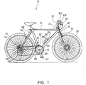
- Fig. 1 is a side view of a bicycle 10 that includes a particular embodiment of a signal processing device 12 (Fig. 3) according to the present invention.
- Bicycle 10 has a frame 14, a front fork 18 rotatably supported in a head tube 22 of frame 14, a front wheel 26 rotatably supported by fork 18, a handlebar 30 for rotating fork 18 (and hence front wheel 26) in the desired direction, and a rear wheel 34 rotatably supported at the rear of frame 14.
- a pair of crank arms 38, each supporting a pedal 42, are mounted to an axle 46 that is rotatably supported in a lower portion of frame 14.
- a plurality of front sprockets 50 are mounted to the right side crank arm 38 for rotating with the right side crank arm 38, and a plurality of rear sprockets 54 are mounted to the rear wheel 34 for rotating with rear wheel 34.
- a chain 58 engages one of the front sprockets 50 and one of the rear sprockets 54.
- a front derailleur 62 is mounted to frame 14 in close proximity to the plurality of front sprockets 50 for moving chain 58 among the plurality of front sprockets 50
- a rear derailleur 66 is mounted to frame 14 in close proximity to the plurality of rear sprockets 54 for moving chain 58 among the plurality of rear sprockets 54.
- a front braking unit 70 is mounted to fork 18 for braking front wheel 26, and a rear braking unit 74 is mounted to the rear of frame 14 for braking rear wheel 34.
- Front braking unit 70 is connected to a Bowden-type control cable 78 that is connected to a brake lever assembly 82 mounted on the right side of handlebar 30 as shown in Fig. 2.
- rear braking unit 74 is connected to a Bowden-type control cable 88 that is connected to a brake lever assembly 92 mounted on the left side of handlebar 30.
- a display housing 100 having an LCD display 104 is coupled to a mounting bracket 108 attached to handlebar 30.
- display housing 100 houses a backlight 112 for display 104, a processor 116 for controlling the operation of display 104, a real time clock (RTC) circuit 120 for providing timing information, a battery 124 for providing backup power for the data stored in processor 116, a receiver circuit 128 for receiving data in a manner described below, a power circuit 132 for receiving power in a manner described below, a resistance (e.g., resistor) R8 coupled to processor 116, and a switch 138 having a terminal 142 coupled to a node 144 between resistance R8 and processor 116 for selecting the information displayed on display 104.
- the other terminal 146 of switch 138 is connected to a ground potential.
- Mounting bracket 108 houses serially connected resistances (e.g., resistors) R1 and R2, a buffer amplifier 150 having an input terminal 154 connected to a node 156 between resistances R1 and R2, a voltage regulator 158 for supplying a regulated voltage to buffer amplifier 150, a voltage regulator 162 for supplying a regulated voltage to resistance R1, and a connector 166.
- resistances e.g., resistors
- Connector 166 includes an external output terminal 170 connected to an output terminal 174 of buffer amplifier 150, a power/data input terminal 178 for communicating power to voltage regulators 158 and 162 in mounting bracket 108 and to power circuit 132 in display housing 100 and for communicating data to receiver circuit 128 in display housing 100, and a ground terminal 182 for providing a ground potential to the components in mounting bracket 108 and display housing 100.
- External output terminal 170, power/data input terminal 178 and ground terminal 182 have exposed contact surfaces 170a, 178a and 182a, respectively.
- the relevant signal processing elements within display housing 100 are directly connected to the relevant signal processing elements within mounting bracket 108.
- display housing 100 may be detachably mounted to mounting bracket 108 in a known manner, wherein exposed electrical contacts (in electrical communication with the relevant components in display housing 100) on display housing 100 contact exposed electrical contacts (in electrical communication with the relevant components in mounting bracket 108) on mounting bracket 108.
- a right switch housing 190 containing a mode switch 194, a rear derailleur upshift switch 198, a rear derailleur downshift switch 202 and serially connected resistances (e.g., resistors) R3 and R4 is mounted to the right side of handlebar 30.
- the relevant signal processing elements within right switch housing 190 are coupled to an intermediate communication path 206 which, in this embodiment, comprises a ground potential communication path 210, a resistance communication path 214 and a resistance communication path 218. More specifically, ground potential communication path 210 is connected to a terminal 222 of mode switch 194, to a terminal 226 of rear derailleur upshift switch 198 and to a terminal 230 of rear derailleur downshift switch 202.
- Another terminal 234 of mode switch 194 is connected to a node 236 on resistance communication path 214 near resistance R3, another terminal 238 of rear derailleur upshift switch 198 is connected to a node 240 between resistances R3 and R4, and another terminal 242 of rear derailleur downshift switch 202 is connected to a node 244 on resistance communication path 218 near resistance R4.
- a left switch housing 250 containing a mode switch 254, a front derailleur upshift switch 258, a front derailleur downshift switch 262 and serially connected resistances (e.g., resistors) R5, R6 and R7 is mounted to the left side of handlebar 30.
- the relevant signal processing elements within left switch housing 250 are coupled to an intermediate communication path 266 which, in this embodiment, comprises a ground potential communication path 270, a resistance communication path 274 and a resistance communication path 278. More specifically, ground potential communication path 270 is connected to a terminal 282 of mode switch 254, to a terminal 286 of front derailleur upshift switch 258 and to a terminal 290 of front derailleur downshift switch 262.
- Another terminal 294 of mode switch 254 is connected to a node 296 between resistances R5 and R6, another terminal 298 of front derailleur upshift switch 258 is connected to a node 300 between resistances R6 and R7, and another terminal 302 of front derailleur downshift switch 262 is connected to a node 304 on resistance communication path 278 near resistance R7.
- Resistance communication path 274 is connected to resistance R5.
- a front derailleur control housing 310 is mounted to frame 14, and it is coupled to mounting bracket 108 through an intermediate communication path 314.
- a rear derailleur control housing 315 is mounted to rear derailleur 66, and it is electrically coupled to front derailleur control housing 310 through an intermediate communication path 316. As shown in Fig.
- front derailleur control housing 310 contains a processor 318, a rectifier and charge control circuit 322 for receiving current from a hub dynamo 326 mounted to rear wheel 34 (not shown) through a communication path 330 and for supplying power to processor 318 through a communication path 330, a capacitance (e.g., capacitor) 334 coupled to rectifier and charge control circuit 322 through a communication path 338 for providing power to other circuit elements as described below, and a programmable memory 342 for storing the programming for processor 318.
- a crank sensor 343 coupled to processor 318 through a communication path 344 is provided for sensing signals from a magnet (not shown) coupled to the left side crank arm 38.
- An optional motor driver 346 is coupled to processor 318 through a communication path 350 for controlling the operation of a motor 354 through a communication path 362 for adjusting an optional front suspension 358
- an optional motor driver 364 is coupled to processor 318 through a communication path 368 for controlling the operation of a motor 372 through a communication path 380 for adjusting an optional rear suspension 376.
- a contact sensor shown as contacts 384a, 384b and 384c is coupled to processor 318 through a communication path 388 for providing signals indicating the position of a front derailleur motor 400 used to position front derailleur 62.
- a motor driver 392 is coupled to processor 318 through a communication path 396 for controlling the operation of front derailleur motor 400 through a communication path 404.
- Motor driver 392 also provides signals over a communication path 408, which is part of intermediate communication path 316, for controlling the operation of a rear derailleur motor 412 contained in rear derailleur control housing 315.
- a potentiometer 416 contained in rear derailleur control housing 315 is coupled to processor 318 through a communication path 420, which is part of intermediate communication path 316, for providing signals indicating the position of motor 412, and hence rear derailleur 66.
- a power/data transmitter 430 is coupled to processor 318 through a communication path 434 for providing power and data signals through a communication path 442 to an external power/data output terminal 438 having a contact surface 438a.
- An external switch signal input terminal 446 having a contact surface 446a is coupled to processor 318 through a communication path 450, and a ground terminal 454 having a contact surface 454a is used to communicate a ground potential among the components in front derailleur control housing 310. Terminals 438, 446 and 454 form part of a connector 456.
- front derailleur control housing 310 is electrically connected to mounting bracket 108 through an intermediate communication path 314.
- Intermediate communication path 314 includes a connector 460 that couples to connector 166 on mounting bracket 108, a connector 464 that couples to connector 456 on front derailleur control housing 310, an intermediate ground potential communication path 468, an intermediate power/data communication path 472, and an intermediate switch signal communication path 476.
- each communication path 468, 472 and 476 comprises a wire, but of course one or more of these communication paths may be an optical communication element or be replaced by a wireless communication method.
- connector 460 includes connector terminals 480, 484 and 488 with contact surfaces 480a, 484a and 488a for contacting the respective contact surfaces 170a, 178a and 182a of external output terminal 170, power/data input terminal 178 and ground terminal 182.
- connector 464 includes terminals 492, 496 and 498 with contact surfaces 492a, 496a and 498a for contacting the respective contact surfaces 446a, 438a and 454a of switch signal input terminal 446, power/data output terminal 438 and ground terminal 454.
- signal processing device 500 includes a housing 504 containing a signal processing element 508 (a switch, sensor, etc.) connected to a processor 512 through a communication path 516, a housing 520 containing a processor 524, and an intermediate communication path 526.
- Processor 512 is connected to external terminals 528, 532 and 536 having respective contact surfaces 528a, 532a and 536a.
- processor 524 is connected to external terminals 540, 544 and 548 having respective contact surfaces 540a, 544a and 548a.
- Terminals 528, 532 and 536 form part of a connector 538, and terminals 540, 544 and 548 form part of a connector 550.
- Intermediate communication path 526 includes a connector 580 for coupling to connector 538 on housing 504, a connector 584 for coupling to connector 550 on housing 520, an intermediate ground potential communication path 588, an intermediate power communication path 592, and an intermediate data signal communication path 596.
- Intermediate ground potential communication path 588 is shown coupled to a ground potential because the ground potential need not originate in processor 512 or processor 524. Such a ground potential may exist at the terminal of a power supply, at the metallic or other conductive elements forming housings 504 and/or 520, or even the bicycle frame or other conductive components attached to the bicycle.
- Each communication path 588, 592 and 596 typically comprises a wire.
- the signals on communication paths 592 and 596 typically are high impedance signals, and very little current flows through them.
- Connector 580 includes connector terminals 600, 604 and 608 with contact surfaces 600a, 604a and 608a for contacting the respective contact surfaces 528a, 532a and 536a of terminals 528, 532 and 536.
- connector 584 includes terminals 612, 616 and 620 with contact surfaces 612a, 616a and 620a for contacting the respective contact surfaces 540a, 544a and 548a of external terminals 540, 544 and 548.
- connectors 580 and 584 be constructed to provide a waterproof seal. This not only increases the initial cost of the device, but over time the connectors may lose their waterproof quality, thus requiring replacement of the connectors, if not the entire device.
- Fig. 5 is a conceptual schematic diagram showing how the circuit of Fig. 4 is modified in accordance with the principles of the present invention.
- signal processing element 508 is not connected through processor 512 (processor 512 has been omitted from the diagram, but processor 512 still may be connected for communicating with intermediate communication paths 588 and 592 as shown in Fig. 4).
- signal processing element 508 is connected to intermediate data signal communication path 596 through an impedance converting circuit 630 that converts the high impedance switch signal appearing on communication path 516' into a low impedance switch signal that is communicated on intermediate data signal communication path 596.
- impedance converting circuit 630 may be an operational amplifier 632 having an input terminal 634 connected to communication path 516', an output terminal 638 connected to external terminal 528, and an input terminal 642 connected to a feedback path 643 that is connected to a node 644 between output terminal 638 and external output terminal 528.
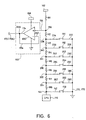
- Fig. 6 is a detailed schematic diagram showing how the principles of the present invention are applied to the device shown in Fig. 3.
- Buffer 150 functions as an impedance converting circuit, and in this embodiment it comprises an operational amplifier 650 having the input terminal 154 connected to the node 156 between resistances R1 and R2, the output terminal 174 connected to external output terminal 170, and an input terminal 652 connected to a feedback path 654 that is connected to a node 656 between output terminal 174 and external output terminal 170.
- operational amplifier 650 is configured as a noninverting, unity gain amplifier.
- Buffer 150 converts the high impedance signal at input terminal 154 into a low impedance signal at output terminal 174.
- the signal at output terminal 174 has an impedance of substantially zero.
- Resistances R1-R8 are connected together in series, with switches 194, 198, 202, 254, 258 and 262 each having one terminal connected to a node 236, 240, 244, 296, 300 and 304, respectively, between adjacent pairs of the resistances.
- the other terminals of switches 194, 198, 202, 254, 258 and 262 are connected to the ground potential appearing on ground potential communication paths 210 and 270.
- Resistances R1-R8 thus function as a voltage divider such that the analog voltage appearing at input terminal 154 of operational amplifier 650 (and hence output terminal 174 of operational amplifier) will vary depending upon which switch 194, 198, 202, 254, 258 and 262 is closed.
- resistances R1-R8 have values of 10k, 2.2k, 2.2k, 2.2k, 3.3k, 5.6k, 8.2k and 18k ohms, respectively.
- operational amplifier 650 Because the varying voltage signal set by the switches 194, 198, 202, 254, 258 and 262 and appearing at output terminal 174 of operational amplifier 650 is a low impedance signal, it will be substantially unaffected by any water that enters between connectors 166 and 460 and/or connectors 456 and 464. Also, the switch signals may be communicated directly to the processor 318 in front derailleur control housing 310. Thus, it is not necessary to incur the expense of using a separate processor to process the switch signals as in the prior art. Operational amplifier 650 also stabilizes the voltages for use by processor 318 (e.g., 10 millivolts either way).
- the present device shown in Fig. 3 is constructed to eliminate such separate communication paths and to communicate power and data over a single communication path. More specifically, the device shown in Fig. 3 includes power/data transmitter 430 in front derailleur control housing 310 for communicating power and data over communication path 442, then to intermediate power/data communication path 472, and ultimately to receiver circuit 128 and power circuit 132 in display housing 100.
- Transmitter 430 comprises a switching circuit 700, a gate drive circuit 704, and a signal shaping circuit 708.
- Switching circuit 700 comprises a field-effect transistor 712 having a gate terminal 716, a source terminal 720 coupled for receiving a voltage Vcc from capacitance 334 (Fig. 4), and a drain terminal 724 coupled to communication path 442.
- Gate drive circuit 704 controls the operation of switching circuit 700, and it includes NPN bipolar transistors Q3, Q6, Q7 and Q8, resistances (e.g., resistors) R9, R10 and R11, and diode D1.
- Transistor Q3 has a collector terminal 728 coupled for receiving voltage Vcc, a base terminal 732 connected to a node 734 between a terminal 736 of resistance R9 and a collector terminal 740 of transistor Q6, and an emitter terminal 744 connected to an anode terminal 748 of diode D1.
- the other terminal 750 of resistance R9 is coupled for receiving voltage Vcc.
- Transistor Q6 further has a base terminal 752 connected to a node 754 on communication path 434a from processor 318, and an emitter terminal 760 connected to a node 765 between a base terminal 764 of transistor Q7 and a terminal 768 of resistance R10.
- the other terminal 770 of resistance R10 is coupled to a ground potential.
- Transistor Q7 further has a collector terminal 772 connected to a node 774 between gate terminal 716 and a cathode terminal 776 of diode D1, and an emitter terminal 780 coupled to a ground potential.
- Transistor Q8 further has a base terminal 784 connected to a terminal 788 of resistance R11, and an emitter terminal 792 coupled to a ground potential.
- the other terminal 796 of resistance R11 is connected to a node 798 between communication path 434b from processor 318 and a terminal 799 of resistance R12.
- Signal shaping circuit 708 shapes the signal appearing at drain terminal 724 of transistor 712 of switching circuit 700, and it includes NPN bipolar transistors Q4 and Q5.
- Transistor Q4 includes a collector terminal 800 connected to a node 802 between drain terminal 724 of transistor 712 and a collector terminal 804 of transistor Q5, a base terminal 808 connected to the other terminal 812 of resistance R12, and an emitter terminal 816 connected to a base terminal 820 of transistor Q5.
- the emitter terminal 824 of transistor Q5 is coupled to a ground potential.
- transmitter 430 may be understood by the signals shown in Figs. 8(A) - 8(D).
- Lower voltage switching signals shown in Fig. 8(A) (approximately 3.0 volts) are produced by processor 318 on communication path 434(A) (point (A) in Fig. 7(A)), and such signals cause gate drive circuit 704 to produce the higher voltage gate drive signals shown in Fig. 8(B) (approximately 4.5 volts) at gate terminal 716 of transistor 712 (point (B)) to operate switching circuit 700.
- switching circuit 700 produces the signals shown in Figs. 8(C) and 8(D) at drain terminal 724 (point (C)).
- Processor 318 produces the signals on communication path 434b to operate signal shaping circuit 708.
- the signals on communication path 434b are similar to the signals produced on communication path 434a (Fig. 8(A)) and are substantially the complements (opposites) of the signals produced on communication path 434a (taking into account propagation delay and necessary timing). These signals, through the operation of transistor Q8, ensure that gate drive circuit 704 rapidly shuts off transistor 712.
- the signals on communication path 434b also cause signal shaping circuit 708 to rapidly sink current from drain terminal 724 of transistor 712 to produce a signal on communication path 442 (point (D)) that more nearly resembles a square wave as shown in Fig. 8(E).
- the signals shown are for example only. In reality, the signals will have varying pulse widths. Also, in this embodiment the pulses should have a frequency greater than 20 Hz to avoid flicker in the display and other artifacts, but in other embodiments that may not be necessary.
- receiver circuit 128 comprises transistors Q1 and Q2 and resistances (e.g., resistors) R13, R14, R15 and R16.
- Transistor Q1 has a collector terminal 850 connected to a node 854 between a power line 858 and a terminal 862 of resistance R14, a base terminal 866 connected to a terminal 870 of resistance R13, and an emitter terminal 874 connected to a node 878 between a terminal 882 of resistance R15 and a terminal 886 of resistance R16.
- the other terminal 886 of resistance R13 is coupled through mounting bracket 108 to power/data input terminal 178, and the other terminal 890 of resistance R16 is coupled to a ground potential.
- Transistor Q2 has a collector terminal 894 connected to a node 898 between the other terminal 902 of resistance R14 and a communication path 906 to processor 116, a base terminal 910 coupled to the other terminal 912 of resistance R15, and an emitter terminal 916 coupled to a ground potential.
- Power circuit 132 comprises a commercially available voltage regulator 920, capacitances (e.g., capacitors) C1-C3, and a diode D2.
- Diode D2 has an anode terminal 924 coupled through mounting bracket 108 to power/data input terminal 178 and a cathode terminal 928 connected to a node 932 between terminals 936 and 940 of capacitances C1 and C3 and an input terminal 944 of voltage regulator 920.
- the other terminals 948 and 952 of capacitances C1 and C3 are coupled to a ground potential.
- Voltage regulator 920 has an output terminal 956 coupled to power line 858 for supplying operating voltage to processor 116 and receiver circuit 128, and a ground terminal 960 coupled to a ground potential.
- Capacitance C2 has a terminal 964 connected to a node 966 between output terminal 956 and power line 858, and a terminal 968 coupled to a ground potential.
- receiver circuit 128 and power circuit 132 may be understood by the signals shown in Figs. 8(C) ⁇ 8(F).
- the pulse signals output from switching circuit 700 (Fig. 8(C)) and shaped by signal shaping circuit 708 (Fig. 8(D)) are communicated over the single intermediate power/data communication path 472 and through mounting bracket 108 to receiver circuit 128 and power circuit 132.
- Diode D2 rectifies the incoming signal and charges capacitances C1 and C3 to produce the input signal shown in Fig. 8(E) on input terminal 944 (point (E)).
- Voltage regulator 920 and capacitance C2 thereafter produce a stable signal (approximately 3 volts) on output terminal 956.
- the power signal is communicated to processor 116 and receiver circuit 128 through power line 858.
- Receiver circuit 128 demodulates the incoming signal and produces the data signal shown in Fig. 8(F) (approximately 3 volts) on communication path 906 (point (F)).
- FIG. 9 is a block diagram of such an alternative embodiment of a transmitter 950 for communicating power and data from a first signal processing element to a second signal processing element.
- a processor 954 controls a sine wave (or other waveform) generator 958 through a communication path 962.
- the generated waveform is communicated to a mixing circuit 966 through a communication path 970.
- Mixer 966 receives power from a power source 974 through a communication path 978, combines the power and waveform signals, and communicates the combined signals on a communication path 982.
- the frequency of the waveform should be less than 500 KHz to avoid radio interference or other artifacts, but that may not be necessary in other embodiments.
- the size, shape, location or orientation of the various components may be changed as desired. Components that are shown directly connected or contacting each other may have intermediate structures disposed between them. The functions of one element may be performed by two, and vice versa. While an operational amplifier was used as an impedance converting circuit in the preferred embodiment, many other circuit elements could be used. For example, bipolar transistors having an emitter-follower configuration could replace operational amplifier 650. The number of switches and resistances will depend upon the application and their assigned function. Power and data communication could occur bidirectionally. It is not necessary for all advantages to be present in a particular embodiment at the same time.
Landscapes
- Engineering & Computer Science (AREA)
- Power Engineering (AREA)
- Physics & Mathematics (AREA)
- General Physics & Mathematics (AREA)
- Mechanical Engineering (AREA)
- Arrangements For Transmission Of Measured Signals (AREA)
Abstract
A bicycle signal processing device 12 includes a first bicycle signal processing element that
generates a first signal having a first impedance, an external output terminal having an exposed
output contact surface, and an impedance converting circuit 150 coupled between the
first bicycle signal processing element and the external output terminal 170 for converting the
first signal to a second signal having a second impedance at the external output terminal 170.
Description
- The present invention is directed to bicycles and, more particularly, to a bicycle signal processing device that operates more reliably in the bicycling environment.
- Many bicycle signal processing systems have been developed. A typical system often gathers and displays information related to bicycle speed, cadence, distance traveled and the like. Such systems usually include a magnet mounted to a wheel spoke, a magnet mounted to one of the pedal cranks, and magnet sensors mounted to the bicycle frame for sensing the passage of the magnets as the wheel and crank revolve. An electrical pulse is generated every time a magnet passes its associated sensor (e.g., once per wheel or crank revolution). The speed of the bicycle can be calculated based on the number of pulses received from the wheel sensor per unit of time and the circumference of the wheel. Similarly, the distance traveled can be calculated based on the number of pulses received over a length of time and the circumference of the wheel. The cadence can be calculated based on the number of pulses received from the crank sensor per unit of time. One or more switches ordinarily are provided for entering operating parameters (e.g., the wheel circumference), for selecting what information is displayed to the rider, and for starting and stopping various timers used for calculating the desired information.
- More sophisticated systems have the ability to display information related to the state of the bicycle transmission. For example, some bicycles have a plurality of front sprockets that rotate with the pedal cranks, a plurality of rear sprockets that rotate with the rear wheel, and a chain that engages one of the front sprockets and one of the rear sprockets. A front derailleur is mounted to the bicycle frame for shifting the chain among the plurality of front sprockets, and a rear derailleur is mounted to the bicycle frame for shifting the chain among the plurality of rear sprockets. Manually operated switches or levers may control the front and rear derailleurs. Position sensors (e.g., potentiometers or contact sensors) are mounted to the switches or levers so that the front and rear sprockets currently engaged by the chain may be determined by the positions of the corresponding switches or levers. Such information may be displayed to the rider so that the rider may operate the transmission accordingly. Even more sophisticated systems use small electric motors to control the bicycle transmission. The motors may be controlled manually by the foregoing switches or levers, or automatically based on bicycle speed and/or cadence.
- The switches, sensors and other electrical components of the signal processing system are often spaced apart from each other and are connected by wires. Not surprisingly, it is desirable to construct the system such that the components are easily installed and removed and to ensure that the electrical signals are reliably communicated from one component to another. To facilitate assembly and removal of the components, it is common to construct the signal processing system as a modular unit, wherein the individual components are connected to each other using detachable electrical connectors. However, when a bicycle is ridden in a wet environment, moisture may enter the connector and form a conductive path to other electrical components or to the frame, thus causing a short circuit or otherwise altering the signals communicated along the wires. The effect is particularly severe when the signals communicated along the wires are high impedance signals. Because of the small amount of current associated with such high impedance signals, a very small amount of current flowing away from a signal wire can result in a large effect on the signal traveling through that wire, usually in the form of an unacceptably large change in signal voltage. As a result, waterproof connectors must be used to connect the components together, thus increasing the cost of the device.
- Finally, because the number of components may be large, it is usually desirable to minimize the number of wires running along the bicycle. Such minimization of wiring not only decreases the cost of the device but also minimizes the number of connectors needed to connect the device together.
- The present invention is directed to a bicycle signal processing device which communicates information from one signal processing element to another signal processing element more reliably than known systems. In one embodiment of the present invention, a bicycle signal processing device includes a first bicycle signal processing element that generates a first signal having a first impedance, an external output terminal having an exposed output contact surface, and an impedance converting circuit coupled between the first bicycle signal processing element and the external output terminal for converting the first signal to a second signal having a second impedance at the external output terminal.
- In a more specific embodiment, the impedance converting circuit may comprise an operational amplifier coupled between the first bicycle signal processing element and the external output terminal. The operational amplifier could be configured as a noninverting, unity gain amplifier to convert the first signal into a second signal having a lower impedance than the first signal.
-
- Fig. 1 is a side view of a bicycle that includes a particular embodiment of a signal processing device according to the present invention;
- Fig. 2 is an oblique view of the handlebar mounted components of the signal processing device;
- Fig. 3 is a detailed block diagram of a particular embodiment of a signal processing device according to the present invention;
- Fig. 4 is conceptual schematic diagram of a prior art signal processing device;
- Fig. 5 is a conceptual schematic diagram showing a particular embodiment of an impedance converting circuit according to the present invention;
- Fig. 6 is a schematic diagram of a particular embodiment of a signal processing element and impedance converting circuit according to the present invention;
- Figs. 7(A) and 7(B) together comprise a schematic diagram of a circuit for communicating power and data from a first signal processing element to a second signal processing element;
- Figs. 8(A)-8(F) are diagrams showing the waveforms of signals at various points in the circuit shown in Figs. 7(A) and 7(B); and
- Fig. 9 is a block diagram of an alternative embodiment of a device for communicating power and data from a first signal processing element to a second signal processing element.
-
- Fig. 1 is a side view of a
bicycle 10 that includes a particular embodiment of a signal processing device 12 (Fig. 3) according to the present invention.Bicycle 10 has aframe 14, afront fork 18 rotatably supported in ahead tube 22 offrame 14, afront wheel 26 rotatably supported byfork 18, ahandlebar 30 for rotating fork 18 (and hence front wheel 26) in the desired direction, and arear wheel 34 rotatably supported at the rear offrame 14. A pair ofcrank arms 38, each supporting apedal 42, are mounted to anaxle 46 that is rotatably supported in a lower portion offrame 14. A plurality offront sprockets 50 are mounted to the rightside crank arm 38 for rotating with the rightside crank arm 38, and a plurality ofrear sprockets 54 are mounted to therear wheel 34 for rotating withrear wheel 34. Achain 58 engages one of thefront sprockets 50 and one of therear sprockets 54. Afront derailleur 62 is mounted toframe 14 in close proximity to the plurality offront sprockets 50 for movingchain 58 among the plurality offront sprockets 50, and arear derailleur 66 is mounted toframe 14 in close proximity to the plurality ofrear sprockets 54 for movingchain 58 among the plurality ofrear sprockets 54. Afront braking unit 70 is mounted tofork 18 for brakingfront wheel 26, and arear braking unit 74 is mounted to the rear offrame 14 for brakingrear wheel 34.Front braking unit 70 is connected to a Bowden-type control cable 78 that is connected to abrake lever assembly 82 mounted on the right side ofhandlebar 30 as shown in Fig. 2. Similarly,rear braking unit 74 is connected to a Bowden-type control cable 88 that is connected to abrake lever assembly 92 mounted on the left side ofhandlebar 30. - As shown in Figs. 1-3, a
display housing 100 having anLCD display 104 is coupled to amounting bracket 108 attached tohandlebar 30. As shown in Fig. 3, displayhousing 100 houses abacklight 112 fordisplay 104, aprocessor 116 for controlling the operation ofdisplay 104, a real time clock (RTC)circuit 120 for providing timing information, abattery 124 for providing backup power for the data stored inprocessor 116, areceiver circuit 128 for receiving data in a manner described below, apower circuit 132 for receiving power in a manner described below, a resistance (e.g., resistor) R8 coupled toprocessor 116, and aswitch 138 having aterminal 142 coupled to anode 144 between resistance R8 andprocessor 116 for selecting the information displayed ondisplay 104. Theother terminal 146 ofswitch 138 is connected to a ground potential. -
Mounting bracket 108 houses serially connected resistances (e.g., resistors) R1 and R2, abuffer amplifier 150 having aninput terminal 154 connected to anode 156 between resistances R1 and R2, avoltage regulator 158 for supplying a regulated voltage tobuffer amplifier 150, avoltage regulator 162 for supplying a regulated voltage to resistance R1, and aconnector 166.Connector 166 includes anexternal output terminal 170 connected to anoutput terminal 174 ofbuffer amplifier 150, a power/data input terminal 178 for communicating power tovoltage regulators mounting bracket 108 and topower circuit 132 indisplay housing 100 and for communicating data toreceiver circuit 128 indisplay housing 100, and aground terminal 182 for providing a ground potential to the components inmounting bracket 108 anddisplay housing 100.External output terminal 170, power/data input terminal 178 andground terminal 182 have exposed contact surfaces 170a, 178a and 182a, respectively. - In this embodiment, the relevant signal processing elements within
display housing 100 are directly connected to the relevant signal processing elements withinmounting bracket 108. In other embodiments,display housing 100 may be detachably mounted to mountingbracket 108 in a known manner, wherein exposed electrical contacts (in electrical communication with the relevant components in display housing 100) ondisplay housing 100 contact exposed electrical contacts (in electrical communication with the relevant components in mounting bracket 108) onmounting bracket 108. - A
right switch housing 190 containing amode switch 194, a rearderailleur upshift switch 198, a rearderailleur downshift switch 202 and serially connected resistances (e.g., resistors) R3 and R4 is mounted to the right side ofhandlebar 30. The relevant signal processing elements withinright switch housing 190 are coupled to anintermediate communication path 206 which, in this embodiment, comprises a groundpotential communication path 210, aresistance communication path 214 and aresistance communication path 218. More specifically, groundpotential communication path 210 is connected to aterminal 222 ofmode switch 194, to aterminal 226 of rearderailleur upshift switch 198 and to aterminal 230 of rearderailleur downshift switch 202. Anotherterminal 234 ofmode switch 194 is connected to anode 236 onresistance communication path 214 near resistance R3, anotherterminal 238 of rearderailleur upshift switch 198 is connected to anode 240 between resistances R3 and R4, and anotherterminal 242 of rearderailleur downshift switch 202 is connected to anode 244 onresistance communication path 218 near resistance R4. - A
left switch housing 250 containing amode switch 254, a frontderailleur upshift switch 258, a frontderailleur downshift switch 262 and serially connected resistances (e.g., resistors) R5, R6 and R7 is mounted to the left side ofhandlebar 30. The relevant signal processing elements withinleft switch housing 250 are coupled to anintermediate communication path 266 which, in this embodiment, comprises a groundpotential communication path 270, aresistance communication path 274 and aresistance communication path 278. More specifically, groundpotential communication path 270 is connected to aterminal 282 ofmode switch 254, to aterminal 286 of frontderailleur upshift switch 258 and to aterminal 290 of frontderailleur downshift switch 262. Anotherterminal 294 ofmode switch 254 is connected to anode 296 between resistances R5 and R6, anotherterminal 298 of frontderailleur upshift switch 258 is connected to anode 300 between resistances R6 and R7, and anotherterminal 302 of frontderailleur downshift switch 262 is connected to anode 304 onresistance communication path 278 near resistance R7.Resistance communication path 274 is connected to resistance R5. - As shown in Fig. 1, a front
derailleur control housing 310 is mounted to frame 14, and it is coupled to mountingbracket 108 through anintermediate communication path 314. A rearderailleur control housing 315 is mounted torear derailleur 66, and it is electrically coupled to frontderailleur control housing 310 through anintermediate communication path 316. As shown in Fig. 3, frontderailleur control housing 310 contains aprocessor 318, a rectifier andcharge control circuit 322 for receiving current from ahub dynamo 326 mounted to rear wheel 34 (not shown) through acommunication path 330 and for supplying power toprocessor 318 through acommunication path 330, a capacitance (e.g., capacitor) 334 coupled to rectifier andcharge control circuit 322 through acommunication path 338 for providing power to other circuit elements as described below, and aprogrammable memory 342 for storing the programming forprocessor 318. Acrank sensor 343 coupled toprocessor 318 through acommunication path 344 is provided for sensing signals from a magnet (not shown) coupled to the left side crankarm 38. Anoptional motor driver 346 is coupled toprocessor 318 through acommunication path 350 for controlling the operation of amotor 354 through acommunication path 362 for adjusting anoptional front suspension 358, and anoptional motor driver 364 is coupled toprocessor 318 through acommunication path 368 for controlling the operation of amotor 372 through acommunication path 380 for adjusting an optionalrear suspension 376. A contact sensor shown as contacts 384a, 384b and 384c is coupled toprocessor 318 through acommunication path 388 for providing signals indicating the position of afront derailleur motor 400 used to positionfront derailleur 62. Amotor driver 392 is coupled toprocessor 318 through a communication path 396 for controlling the operation offront derailleur motor 400 through acommunication path 404.Motor driver 392 also provides signals over acommunication path 408, which is part ofintermediate communication path 316, for controlling the operation of arear derailleur motor 412 contained in rearderailleur control housing 315. Apotentiometer 416 contained in rearderailleur control housing 315 is coupled toprocessor 318 through acommunication path 420, which is part ofintermediate communication path 316, for providing signals indicating the position ofmotor 412, and hencerear derailleur 66. - A power/
data transmitter 430 is coupled toprocessor 318 through acommunication path 434 for providing power and data signals through acommunication path 442 to an external power/data output terminal 438 having a contact surface 438a. An external switchsignal input terminal 446 having a contact surface 446a is coupled toprocessor 318 through acommunication path 450, and aground terminal 454 having a contact surface 454a is used to communicate a ground potential among the components in frontderailleur control housing 310.Terminals connector 456. - As noted above, front
derailleur control housing 310 is electrically connected to mountingbracket 108 through anintermediate communication path 314.Intermediate communication path 314 includes aconnector 460 that couples toconnector 166 on mountingbracket 108, aconnector 464 that couples toconnector 456 on frontderailleur control housing 310, an intermediate groundpotential communication path 468, an intermediate power/data communication path 472, and an intermediate switchsignal communication path 476. In this embodiment, eachcommunication path connector 460 includesconnector terminals external output terminal 170, power/data input terminal 178 andground terminal 182. Similarly,connector 464 includesterminals signal input terminal 446, power/data output terminal 438 andground terminal 454. - Before continuing with the description of
signal processing device 12, it may be helpful to consider a prior artsignal processing device 500 shown conceptually in Fig. 4. As shown in Fig. 4,signal processing device 500 includes ahousing 504 containing a signal processing element 508 (a switch, sensor, etc.) connected to aprocessor 512 through acommunication path 516, ahousing 520 containing aprocessor 524, and anintermediate communication path 526.Processor 512 is connected toexternal terminals processor 524 is connected toexternal terminals Terminals connector 538, andterminals connector 550.Intermediate communication path 526 includes aconnector 580 for coupling toconnector 538 onhousing 504, aconnector 584 for coupling toconnector 550 onhousing 520, an intermediate groundpotential communication path 588, an intermediatepower communication path 592, and an intermediate datasignal communication path 596. Intermediate groundpotential communication path 588 is shown coupled to a ground potential because the ground potential need not originate inprocessor 512 orprocessor 524. Such a ground potential may exist at the terminal of a power supply, at the metallic or other conductiveelements forming housings 504 and/or 520, or even the bicycle frame or other conductive components attached to the bicycle. Eachcommunication path communication paths Connector 580 includesconnector terminals terminals connector 584 includesterminals external terminals - If water were to enter between
connector 580 andconnector 538, for example, there is a possibility that the water, being somewhat conductive, will form a conductive path betweencommunication paths 592 and/or 596 and the ground potential. The effect may be similar to current siphoned off through a resistance of, for example, 1K ohms to a ground potential. Since the signals onintermediate communication paths intermediate communication paths processor 524 will vary greatly even if the current lost through the conductive path is small. Indeed, it is possible that a complete short circuit may result. In any event, such a voltage variation may causeprocessor 524 to malfunction. To prevent such malfunctioning, it is necessary thatconnectors - Fig. 5 is a conceptual schematic diagram showing how the circuit of Fig. 4 is modified in accordance with the principles of the present invention. In this case,
signal processing element 508 is not connected through processor 512 (processor 512 has been omitted from the diagram, butprocessor 512 still may be connected for communicating withintermediate communication paths signal processing element 508 is connected to intermediate data signalcommunication path 596 through animpedance converting circuit 630 that converts the high impedance switch signal appearing on communication path 516' into a low impedance switch signal that is communicated on intermediate data signalcommunication path 596. In this example,impedance converting circuit 630 may be anoperational amplifier 632 having aninput terminal 634 connected to communication path 516', anoutput terminal 638 connected toexternal terminal 528, and aninput terminal 642 connected to afeedback path 643 that is connected to anode 644 betweenoutput terminal 638 andexternal output terminal 528. - Fig. 6 is a detailed schematic diagram showing how the principles of the present invention are applied to the device shown in Fig. 3. Buffer 150 functions as an impedance converting circuit, and in this embodiment it comprises an
operational amplifier 650 having theinput terminal 154 connected to thenode 156 between resistances R1 and R2, theoutput terminal 174 connected toexternal output terminal 170, and aninput terminal 652 connected to afeedback path 654 that is connected to anode 656 betweenoutput terminal 174 andexternal output terminal 170. One of ordinary skill in the art will readily recognize that, in this embodiment,operational amplifier 650 is configured as a noninverting, unity gain amplifier. Buffer 150 converts the high impedance signal atinput terminal 154 into a low impedance signal atoutput terminal 174. The signal atoutput terminal 174 has an impedance of substantially zero. - Resistances R1-R8 are connected together in series, with
switches node switches potential communication paths input terminal 154 of operational amplifier 650 (and henceoutput terminal 174 of operational amplifier) will vary depending upon which switch 194, 198, 202, 254, 258 and 262 is closed. In this embodiment, resistances R1-R8 have values of 10k, 2.2k, 2.2k, 2.2k, 3.3k, 5.6k, 8.2k and 18k ohms, respectively. - Because the varying voltage signal set by the
switches output terminal 174 ofoperational amplifier 650 is a low impedance signal, it will be substantially unaffected by any water that enters betweenconnectors connectors processor 318 in frontderailleur control housing 310. Thus, it is not necessary to incur the expense of using a separate processor to process the switch signals as in the prior art.Operational amplifier 650 also stabilizes the voltages for use by processor 318 (e.g., 10 millivolts either way). - As noted above when discussing the prior art device shown in Fig. 4, conventional devices have separate power and data communication paths for communicating power and data from one signal processing element to another. The present device shown in Fig. 3 is constructed to eliminate such separate communication paths and to communicate power and data over a single communication path. More specifically, the device shown in Fig. 3 includes power/
data transmitter 430 in frontderailleur control housing 310 for communicating power and data overcommunication path 442, then to intermediate power/data communication path 472, and ultimately toreceiver circuit 128 andpower circuit 132 indisplay housing 100. - Figs. 7(A) and 7(B) together comprise a detailed schematic diagram of the relevant components of
transmitter 430,receiver circuit 128 andpower circuit 132.Transmitter 430 comprises aswitching circuit 700, a gate drive circuit 704, and asignal shaping circuit 708. -
Switching circuit 700 comprises a field-effect transistor 712 having agate terminal 716, asource terminal 720 coupled for receiving a voltage Vcc from capacitance 334 (Fig. 4), and adrain terminal 724 coupled tocommunication path 442. - Gate drive circuit 704 controls the operation of switching
circuit 700, and it includes NPN bipolar transistors Q3, Q6, Q7 and Q8, resistances (e.g., resistors) R9, R10 and R11, and diode D1. Transistor Q3 has acollector terminal 728 coupled for receiving voltage Vcc, abase terminal 732 connected to anode 734 between a terminal 736 of resistance R9 and acollector terminal 740 of transistor Q6, and anemitter terminal 744 connected to ananode terminal 748 of diode D1. Theother terminal 750 of resistance R9 is coupled for receiving voltage Vcc. Transistor Q6 further has abase terminal 752 connected to anode 754 on communication path 434a fromprocessor 318, and anemitter terminal 760 connected to anode 765 between abase terminal 764 of transistor Q7 and aterminal 768 of resistance R10. Theother terminal 770 of resistance R10 is coupled to a ground potential. Transistor Q7 further has acollector terminal 772 connected to anode 774 betweengate terminal 716 and acathode terminal 776 of diode D1, and anemitter terminal 780 coupled to a ground potential. Transistor Q8 further has abase terminal 784 connected to a terminal 788 of resistance R11, and anemitter terminal 792 coupled to a ground potential. Theother terminal 796 of resistance R11 is connected to anode 798 betweencommunication path 434b fromprocessor 318 and aterminal 799 of resistance R12. - Signal shaping
circuit 708 shapes the signal appearing atdrain terminal 724 oftransistor 712 of switchingcircuit 700, and it includes NPN bipolar transistors Q4 and Q5. Transistor Q4 includes acollector terminal 800 connected to anode 802 betweendrain terminal 724 oftransistor 712 and acollector terminal 804 of transistor Q5, abase terminal 808 connected to theother terminal 812 of resistance R12, and anemitter terminal 816 connected to abase terminal 820 of transistor Q5. Theemitter terminal 824 of transistor Q5 is coupled to a ground potential. - The operation of
transmitter 430 may be understood by the signals shown in Figs. 8(A) - 8(D). Lower voltage switching signals shown in Fig. 8(A) (approximately 3.0 volts) are produced byprocessor 318 on communication path 434(A) (point (A) in Fig. 7(A)), and such signals cause gate drive circuit 704 to produce the higher voltage gate drive signals shown in Fig. 8(B) (approximately 4.5 volts) atgate terminal 716 of transistor 712 (point (B)) to operate switchingcircuit 700. In response, switchingcircuit 700 produces the signals shown in Figs. 8(C) and 8(D) at drain terminal 724 (point (C)).Processor 318 produces the signals oncommunication path 434b to operatesignal shaping circuit 708. The signals oncommunication path 434b are similar to the signals produced on communication path 434a (Fig. 8(A)) and are substantially the complements (opposites) of the signals produced on communication path 434a (taking into account propagation delay and necessary timing). These signals, through the operation of transistor Q8, ensure that gate drive circuit 704 rapidly shuts offtransistor 712. The signals oncommunication path 434b also causesignal shaping circuit 708 to rapidly sink current fromdrain terminal 724 oftransistor 712 to produce a signal on communication path 442 (point (D)) that more nearly resembles a square wave as shown in Fig. 8(E). The signals shown are for example only. In reality, the signals will have varying pulse widths. Also, in this embodiment the pulses should have a frequency greater than 20 Hz to avoid flicker in the display and other artifacts, but in other embodiments that may not be necessary. - As shown in Fig. 7(B),
receiver circuit 128 comprises transistors Q1 and Q2 and resistances (e.g., resistors) R13, R14, R15 and R16. Transistor Q1 has acollector terminal 850 connected to anode 854 between apower line 858 and aterminal 862 of resistance R14, abase terminal 866 connected to aterminal 870 of resistance R13, and anemitter terminal 874 connected to anode 878 between a terminal 882 of resistance R15 and aterminal 886 of resistance R16. Theother terminal 886 of resistance R13 is coupled through mountingbracket 108 to power/data input terminal 178, and theother terminal 890 of resistance R16 is coupled to a ground potential. Transistor Q2 has acollector terminal 894 connected to anode 898 between theother terminal 902 of resistance R14 and acommunication path 906 toprocessor 116, abase terminal 910 coupled to theother terminal 912 of resistance R15, and anemitter terminal 916 coupled to a ground potential. -
Power circuit 132 comprises a commerciallyavailable voltage regulator 920, capacitances (e.g., capacitors) C1-C3, and a diode D2. Diode D2 has ananode terminal 924 coupled through mountingbracket 108 to power/data input terminal 178 and acathode terminal 928 connected to anode 932 betweenterminals input terminal 944 ofvoltage regulator 920. Theother terminals 948 and 952 of capacitances C1 and C3 are coupled to a ground potential.Voltage regulator 920 has anoutput terminal 956 coupled topower line 858 for supplying operating voltage toprocessor 116 andreceiver circuit 128, and aground terminal 960 coupled to a ground potential. Capacitance C2 has a terminal 964 connected to anode 966 betweenoutput terminal 956 andpower line 858, and a terminal 968 coupled to a ground potential. - The operation of
receiver circuit 128 andpower circuit 132 may be understood by the signals shown in Figs. 8(C) ― 8(F). The pulse signals output from switching circuit 700 (Fig. 8(C)) and shaped by signal shaping circuit 708 (Fig. 8(D)) are communicated over the single intermediate power/data communication path 472 and through mountingbracket 108 toreceiver circuit 128 andpower circuit 132. Diode D2 rectifies the incoming signal and charges capacitances C1 and C3 to produce the input signal shown in Fig. 8(E) on input terminal 944 (point (E)).Voltage regulator 920 and capacitance C2 thereafter produce a stable signal (approximately 3 volts) onoutput terminal 956. The power signal is communicated toprocessor 116 andreceiver circuit 128 throughpower line 858.Receiver circuit 128 demodulates the incoming signal and produces the data signal shown in Fig. 8(F) (approximately 3 volts) on communication path 906 (point (F)). - While the above is a description of various embodiments of the present invention, further modifications may be employed without departing from the spirit and scope of the present invention. For example, while pulses were used to communicate data in the preferred embodiment, frequency modulation also could be employed. Fig. 9 is a block diagram of such an alternative embodiment of a
transmitter 950 for communicating power and data from a first signal processing element to a second signal processing element. In this embodiment, aprocessor 954 controls a sine wave (or other waveform)generator 958 through acommunication path 962. The generated waveform is communicated to amixing circuit 966 through acommunication path 970.Mixer 966 receives power from apower source 974 through acommunication path 978, combines the power and waveform signals, and communicates the combined signals on acommunication path 982. In such an embodiment the frequency of the waveform should be less than 500 KHz to avoid radio interference or other artifacts, but that may not be necessary in other embodiments. - The size, shape, location or orientation of the various components may be changed as desired. Components that are shown directly connected or contacting each other may have intermediate structures disposed between them. The functions of one element may be performed by two, and vice versa. While an operational amplifier was used as an impedance converting circuit in the preferred embodiment, many other circuit elements could be used. For example, bipolar transistors having an emitter-follower configuration could replace
operational amplifier 650. The number of switches and resistances will depend upon the application and their assigned function. Power and data communication could occur bidirectionally. It is not necessary for all advantages to be present in a particular embodiment at the same time. Every feature that is unique from the prior art, alone or in combination with other features, also should be considered a separate description of further inventions by the applicant, including the structural and/or functional concepts embodied by such feature(s). Thus, the scope of the invention should not be limited by the specific structures disclosed or the apparent initial focus on a particular structure or feature.
Claims (17)
- A bicycle signal processing device (12) comprising:a first bicycle signal processing element that generates a first signal having a first impedance;an external output terminal (170) having an exposed output contact surface; andan impedance converting circuit (150) coupled between the first bicycle signal processing element and the external output terminal (170) for converting the first signal to a second signal having a second impedance at the external output terminal (170).
- The device (12) according to claim 1 wherein the second impedance is less than the first impedance.
- The device (12) according to claim 1 or 2 wherein the first bicycle signal processing element comprises a voltage divider.
- The device (12) according to claim 3 wherein the voltage divider comprises:a plurality of resistances connected in series; anda switch having a first switch terminal coupled to a node between an adjacent pair of resistances from the plurality of resistances.
- The device (12) according to claim 4 wherein the switch has a second switch terminal directly coupled to a ground potential.
- The device (12) according to any of the preceding claims wherein the first bicycle signal processing element comprises:a mounting member for attaching the first bicycle signal processing element to a bicycle (10);a switch coupled to the mounting member; anda resistance element coupled to the switch.
- The device (12) according to claim 6 wherein the resistance element comprises a voltage divider.
- The device (12) according to claim 7 wherein the voltage divider comprises a plurality of resistances connected in series, wherein the switch has a first switch terminal coupled to a node between an adjacent pair of resistances from the plurality of resistances.
- The device (12) according to any of the preceding claims wherein the impedance converting circuit (150) comprises an operational amplifier (650) coupled between the first bicycle signal processing element and the external output terminal (170).
- The device (12) according to claim 9 wherein the operational amplifier (650) has an input terminal (154) coupled for receiving the first signal and an output terminal (174) coupled to the external output terminal (170).
- The device (12) according to claim 9 or 10 wherein the operational amplifier (650) is configured for unity gain.
- The device (12) according to claims 9 to 11 wherein the operational amplifier (650) is configured as a noninverting amplifier.
- The device (12) according to claims 9 to 12 further comprising an intermediate communication element having a first connector with a first connector terminal with a first terminal contact surface for contacting the output contact surface of the external output terminal (170).
- The device (12) according to claims 9 to 13 further comprising a second bicycle signal processing element coupled to the intermediate communication element for receiving the second signal.
- The device (12) according to claim 14 wherein the second bicycle signal processing element comprises a processor that processes the second signal.
- The device (12) according to claim 14 or 15 wherein the intermediate communication element has a second connector with a second connector terminal with a second terminal contact surface so that the second signal is communicated from the first terminal contact surface to the second terminal contact surface, and wherein the second bicycle signal processing element has an external input terminal having an exposed input contact surface for contacting the second terminal contact surface.
- The device (12) according to claim 15 wherein the processor has a processor input terminal directly connected to the external input terminal.
Applications Claiming Priority (2)
| Application Number | Priority Date | Filing Date | Title |
|---|---|---|---|
| US10/131,151 US7116008B2 (en) | 2002-04-23 | 2002-04-23 | Electrical communication system for a bicycle |
| US131151 | 2002-04-23 |
Publications (1)
| Publication Number | Publication Date |
|---|---|
| EP1357021A2 true EP1357021A2 (en) | 2003-10-29 |
Family
ID=28790977
Family Applications (1)
| Application Number | Title | Priority Date | Filing Date |
|---|---|---|---|
| EP03008501A Withdrawn EP1357021A2 (en) | 2002-04-23 | 2003-04-11 | Electrical communication system for a bicycle |
Country Status (5)
| Country | Link |
|---|---|
| US (2) | US7116008B2 (en) |
| EP (1) | EP1357021A2 (en) |
| JP (1) | JP2003327188A (en) |
| CN (1) | CN100335359C (en) |
| TW (1) | TWI221131B (en) |
Families Citing this family (23)
| Publication number | Priority date | Publication date | Assignee | Title |
|---|---|---|---|---|
| IT1320286B1 (en) * | 2000-03-29 | 2003-11-26 | Campagnolo Srl | MULTIPROCESSOR CONTROL SYSTEM FOR CYCLES, FOR EXAMPLE COMPETITION BICYCLES. |
| US7373845B2 (en) * | 2001-06-19 | 2008-05-20 | Cts Corporation | Seat belt tension sensor |
| US7272979B2 (en) * | 2001-06-19 | 2007-09-25 | Cts Corporation | Seat belt tension sensor having an integral connector |
| US7347108B2 (en) * | 2001-06-19 | 2008-03-25 | Cts Corporation | Seat belt tension sensor |
| JP2004110628A (en) * | 2002-09-20 | 2004-04-08 | Shimano Inc | Bicycle user's information management device and cycle computer |
| US7522033B2 (en) * | 2005-07-27 | 2009-04-21 | Shimano, Inc. | Signal generating apparatus for a bicycle control device |
| ITMI20070140A1 (en) * | 2007-01-30 | 2008-07-31 | Campagnolo Srl | MAN-BICYCLE INTERACTION DEVICE |
| ITMI20070737A1 (en) * | 2007-04-12 | 2008-10-13 | Campagnolo Srl | EQUIPMENT AND ELECTRONIC SYSTEM FOR BICYCLE AND RELATIVE METHODS |
| US20090088934A1 (en) * | 2007-09-28 | 2009-04-02 | Shimano Inc. | Bicycle control system |
| US7902967B2 (en) * | 2007-10-23 | 2011-03-08 | Shimano Inc. | Bicycle control system |
| ITMI20072407A1 (en) * | 2007-12-20 | 2009-06-21 | Campagnolo Srl | ELECTRONIC EQUIPMENT FOR BICYCLE |
| EP2757030B1 (en) | 2008-01-24 | 2015-12-23 | Cycling Sports Group, Inc. | Bicycle user interface system and method of operation thereof |
| US20100010709A1 (en) * | 2008-01-24 | 2010-01-14 | Cannondale Bicycle Corporation | Bicycle distributed computing arrangement and method of operation |
| US7805268B2 (en) * | 2008-02-20 | 2010-09-28 | Shimano Inc. | Bicycle component calibration device |
| US8025597B2 (en) * | 2008-02-20 | 2011-09-27 | Shimano Inc. | Bicycle component position correcting device |
| JP5607003B2 (en) * | 2011-08-29 | 2014-10-15 | 株式会社シマノ | Bicycle sensor control device and bicycle sensor control method |
| US9302739B2 (en) | 2012-06-18 | 2016-04-05 | Shimano, Inc. | Bicycle power control apparatus |
| US9561734B2 (en) | 2012-07-31 | 2017-02-07 | Shimano Inc. | Bicycle power supply system |
| US8909424B2 (en) * | 2012-10-11 | 2014-12-09 | Sram, Llc | Electronic shifting systems and methods |
| JP6305322B2 (en) * | 2014-11-28 | 2018-04-04 | 株式会社シマノ | Components and communication systems |
| US10363992B2 (en) * | 2015-01-29 | 2019-07-30 | Shimano Inc. | Electric bicycle component |
| TWI781303B (en) * | 2015-03-06 | 2022-10-21 | 日商島野股份有限公司 | Bicycle electrical component |
| US11964725B2 (en) | 2021-08-31 | 2024-04-23 | Sram, Llc | Low power control for a control device for a bicycle |
Family Cites Families (30)
| Publication number | Priority date | Publication date | Assignee | Title |
|---|---|---|---|---|
| USRE27983E (en) * | 1972-08-07 | 1974-04-23 | Music synthesizer keyboard | |
| US4143557A (en) * | 1977-04-18 | 1979-03-13 | Sanyo Electric Co., Ltd | Control system for use in a multiple speed transmission system |
| GB2061033B (en) | 1979-06-18 | 1983-11-16 | Ullmann Ulo Werk | Electric lighting apparatus for a bicycle |
| WO1981001274A1 (en) | 1979-11-06 | 1981-05-14 | T Murphy | Bicycle or other vehicle generator improvement unit |
| GB2126438B (en) | 1982-02-10 | 1986-09-17 | Vincent Joseph Skinner | Lighting system for cycles |
| US4962462A (en) * | 1983-09-29 | 1990-10-09 | Engelhard Corporation | Fuel cell/battery hybrid system |
| GB8412897D0 (en) | 1984-05-21 | 1984-06-27 | Mackinnon J M | Electrical power supply device |
| FR2687977B1 (en) * | 1992-02-27 | 1994-04-22 | Bg Innovation | DEVICES ALLOWING THE CHANGES OF SPEEDS ON BICYCLES. |
| DE4212320A1 (en) * | 1992-04-13 | 1993-10-14 | Fichtel & Sachs Ag | Electric actuator |
| US5455774A (en) * | 1992-10-22 | 1995-10-03 | Motorola, Inc. | Interrupt programmable analog-to-digital port |
| US5414335A (en) * | 1993-04-08 | 1995-05-09 | Harada Kogyo Kabushiki Kaisha | Device for controlling the angle of the optical axis of a headlamp light |
| US5612580A (en) * | 1995-10-10 | 1997-03-18 | Northrop Grumman Corporation | Uninterruptible power system |
| JP3088661B2 (en) * | 1996-07-23 | 2000-09-18 | 株式会社シマノ | Method and apparatus for transmitting detection signal in bicycle |
| JPH1065744A (en) | 1996-08-13 | 1998-03-06 | Oki Electric Ind Co Ltd | Bus interface circuit |
| JP3321045B2 (en) * | 1996-12-20 | 2002-09-03 | 株式会社シマノ | Bicycle electrical operating device |
| JP3727751B2 (en) * | 1997-04-18 | 2005-12-14 | 株式会社三社電機製作所 | Bicycle transmission |
| US6192300B1 (en) * | 1997-06-27 | 2001-02-20 | Echowell Electronic Ltd. | Bicycle computer |
| US6122181A (en) * | 1998-05-21 | 2000-09-19 | Exide Electronics Corporation | Systems and methods for producing standby uninterruptible power for AC loads using rectified AC and battery |
| JP3231018B2 (en) * | 1998-06-26 | 2001-11-19 | 株式会社シマノ | Bicycle computer |
| US6222343B1 (en) * | 1998-08-14 | 2001-04-24 | Milwaukee Electric Tool Corporation | Battery charger, a method for charging a battery, and a software program for operating the battery charger |
| DE19948798A1 (en) | 1998-10-10 | 2001-05-10 | Norman Gerkinsmeyer | Bicycle lighting device has dynamo coupled to rechargeable battery and lighting system with front headlamp and rear tail-light |
| US6181263B1 (en) * | 1999-02-26 | 2001-01-30 | Linear Technology Corp. | Signal processor |
| US6163445A (en) * | 1999-03-11 | 2000-12-19 | Fluke Corporation | Low-voltage test signal path protection circuit with extended bandwidth, overvoltage and transient protection |
| IT1310744B1 (en) * | 1999-11-26 | 2002-02-22 | Campagnolo Srl | SENSOR DEVICE FOR THE OPERATIONAL POSITION OF A SPEED CHANGE SYSTEM FOR BICYCLES, AND A SPEED CHANGE SYSTEM |
| IT1320286B1 (en) * | 2000-03-29 | 2003-11-26 | Campagnolo Srl | MULTIPROCESSOR CONTROL SYSTEM FOR CYCLES, FOR EXAMPLE COMPETITION BICYCLES. |
| DE20016669U1 (en) | 2000-09-18 | 2000-12-28 | Braun, Peter, 10627 Berlin | Accu dynamo automatic |
| JP4867066B2 (en) | 2000-11-28 | 2012-02-01 | 日本テキサス・インスツルメンツ株式会社 | Amplifier circuit |
| JP2002164749A (en) | 2000-11-29 | 2002-06-07 | Matsushita Electric Ind Co Ltd | Impedance conversion type amplifier |
| JP2002187584A (en) | 2000-12-22 | 2002-07-02 | Shimano Inc | Drive control circuit for electric bicycle unit |
| US7024482B2 (en) * | 2001-02-28 | 2006-04-04 | Sharp Laboratories Of America, Inc. | Pseudo-random dynamic scheduler for scheduling communication periods between electronic devices |
-
2002
- 2002-04-23 US US10/131,151 patent/US7116008B2/en not_active Expired - Fee Related
-
2003
- 2003-03-25 TW TW092106667A patent/TWI221131B/en not_active IP Right Cessation
- 2003-04-02 US US10/406,424 patent/US20030207731A1/en not_active Abandoned
- 2003-04-11 EP EP03008501A patent/EP1357021A2/en not_active Withdrawn
- 2003-04-21 JP JP2003116281A patent/JP2003327188A/en not_active Ceased
- 2003-04-22 CN CNB031232124A patent/CN100335359C/en not_active Expired - Fee Related
Also Published As
| Publication number | Publication date |
|---|---|
| US7116008B2 (en) | 2006-10-03 |
| TW200307619A (en) | 2003-12-16 |
| TWI221131B (en) | 2004-09-21 |
| US20030197600A1 (en) | 2003-10-23 |
| CN1453181A (en) | 2003-11-05 |
| US20030207731A1 (en) | 2003-11-06 |
| CN100335359C (en) | 2007-09-05 |
| JP2003327188A (en) | 2003-11-19 |
Similar Documents
| Publication | Publication Date | Title |
|---|---|---|
| EP1357678B1 (en) | Bicycle control apparatus that communicates power and data over a single transmission path | |
| EP1391974B1 (en) | Power control apparatus for a bicycle | |
| EP1357021A2 (en) | Electrical communication system for a bicycle | |
| EP1375324B1 (en) | Bicycle data communication method and apparatus | |
| EP1394031B1 (en) | Apparatus for wiring bicycle electrical components | |
| TW202128492A (en) | Interface for electric assist bicycle | |
| US7147238B2 (en) | Bicycle part with a partitioned chamber | |
| EP1398266B1 (en) | Bicycle power supply | |
| US20210061413A1 (en) | Bicycle derailleur | |
| EP2873603B1 (en) | Bicycle electronic system |
Legal Events
| Date | Code | Title | Description |
|---|---|---|---|
| PUAI | Public reference made under article 153(3) epc to a published international application that has entered the european phase |
Free format text: ORIGINAL CODE: 0009012 |
|
| AK | Designated contracting states |
Kind code of ref document: A2 Designated state(s): AT BE BG CH CY CZ DE DK EE ES FI FR GB GR HU IE IT LI LU MC NL PT RO SE SI SK TR |
|
| AX | Request for extension of the european patent |
Extension state: AL LT LV MK |
|
| STAA | Information on the status of an ep patent application or granted ep patent |
Free format text: STATUS: THE APPLICATION HAS BEEN WITHDRAWN |
|
| 18W | Application withdrawn |
Effective date: 20060512 |