EP1353319A1 - Dual scan method of matrix display panel - Google Patents
Dual scan method of matrix display panel Download PDFInfo
- Publication number
- EP1353319A1 EP1353319A1 EP03007770A EP03007770A EP1353319A1 EP 1353319 A1 EP1353319 A1 EP 1353319A1 EP 03007770 A EP03007770 A EP 03007770A EP 03007770 A EP03007770 A EP 03007770A EP 1353319 A1 EP1353319 A1 EP 1353319A1
- Authority
- EP
- European Patent Office
- Prior art keywords
- scan
- scan lines
- lower half
- lines
- display panel
- Prior art date
- Legal status (The legal status is an assumption and is not a legal conclusion. Google has not performed a legal analysis and makes no representation as to the accuracy of the status listed.)
- Withdrawn
Links
- 230000009977 dual effect Effects 0.000 title claims abstract description 21
- 238000000034 method Methods 0.000 title claims abstract description 21
- 239000011159 matrix material Substances 0.000 title description 12
- 230000008901 benefit Effects 0.000 description 4
- 238000010586 diagram Methods 0.000 description 4
- 238000012986 modification Methods 0.000 description 2
- 230000004048 modification Effects 0.000 description 2
- 238000011161 development Methods 0.000 description 1
- 230000018109 developmental process Effects 0.000 description 1
- 238000005401 electroluminescence Methods 0.000 description 1
- 239000004973 liquid crystal related substance Substances 0.000 description 1
- 238000004519 manufacturing process Methods 0.000 description 1
- 239000000463 material Substances 0.000 description 1
- 230000035807 sensation Effects 0.000 description 1
- 230000000007 visual effect Effects 0.000 description 1
Images


Classifications
-
- G—PHYSICS
- G09—EDUCATION; CRYPTOGRAPHY; DISPLAY; ADVERTISING; SEALS
- G09G—ARRANGEMENTS OR CIRCUITS FOR CONTROL OF INDICATING DEVICES USING STATIC MEANS TO PRESENT VARIABLE INFORMATION
- G09G3/00—Control arrangements or circuits, of interest only in connection with visual indicators other than cathode-ray tubes
- G09G3/20—Control arrangements or circuits, of interest only in connection with visual indicators other than cathode-ray tubes for presentation of an assembly of a number of characters, e.g. a page, by composing the assembly by combination of individual elements arranged in a matrix no fixed position being assigned to or needed to be assigned to the individual characters or partial characters
- G09G3/22—Control arrangements or circuits, of interest only in connection with visual indicators other than cathode-ray tubes for presentation of an assembly of a number of characters, e.g. a page, by composing the assembly by combination of individual elements arranged in a matrix no fixed position being assigned to or needed to be assigned to the individual characters or partial characters using controlled light sources
- G09G3/30—Control arrangements or circuits, of interest only in connection with visual indicators other than cathode-ray tubes for presentation of an assembly of a number of characters, e.g. a page, by composing the assembly by combination of individual elements arranged in a matrix no fixed position being assigned to or needed to be assigned to the individual characters or partial characters using controlled light sources using electroluminescent panels
-
- G—PHYSICS
- G09—EDUCATION; CRYPTOGRAPHY; DISPLAY; ADVERTISING; SEALS
- G09G—ARRANGEMENTS OR CIRCUITS FOR CONTROL OF INDICATING DEVICES USING STATIC MEANS TO PRESENT VARIABLE INFORMATION
- G09G3/00—Control arrangements or circuits, of interest only in connection with visual indicators other than cathode-ray tubes
- G09G3/20—Control arrangements or circuits, of interest only in connection with visual indicators other than cathode-ray tubes for presentation of an assembly of a number of characters, e.g. a page, by composing the assembly by combination of individual elements arranged in a matrix no fixed position being assigned to or needed to be assigned to the individual characters or partial characters
- G09G3/22—Control arrangements or circuits, of interest only in connection with visual indicators other than cathode-ray tubes for presentation of an assembly of a number of characters, e.g. a page, by composing the assembly by combination of individual elements arranged in a matrix no fixed position being assigned to or needed to be assigned to the individual characters or partial characters using controlled light sources
- G09G3/30—Control arrangements or circuits, of interest only in connection with visual indicators other than cathode-ray tubes for presentation of an assembly of a number of characters, e.g. a page, by composing the assembly by combination of individual elements arranged in a matrix no fixed position being assigned to or needed to be assigned to the individual characters or partial characters using controlled light sources using electroluminescent panels
- G09G3/32—Control arrangements or circuits, of interest only in connection with visual indicators other than cathode-ray tubes for presentation of an assembly of a number of characters, e.g. a page, by composing the assembly by combination of individual elements arranged in a matrix no fixed position being assigned to or needed to be assigned to the individual characters or partial characters using controlled light sources using electroluminescent panels semiconductive, e.g. using light-emitting diodes [LED]
- G09G3/3208—Control arrangements or circuits, of interest only in connection with visual indicators other than cathode-ray tubes for presentation of an assembly of a number of characters, e.g. a page, by composing the assembly by combination of individual elements arranged in a matrix no fixed position being assigned to or needed to be assigned to the individual characters or partial characters using controlled light sources using electroluminescent panels semiconductive, e.g. using light-emitting diodes [LED] organic, e.g. using organic light-emitting diodes [OLED]
- G09G3/3216—Control arrangements or circuits, of interest only in connection with visual indicators other than cathode-ray tubes for presentation of an assembly of a number of characters, e.g. a page, by composing the assembly by combination of individual elements arranged in a matrix no fixed position being assigned to or needed to be assigned to the individual characters or partial characters using controlled light sources using electroluminescent panels semiconductive, e.g. using light-emitting diodes [LED] organic, e.g. using organic light-emitting diodes [OLED] using a passive matrix
-
- G—PHYSICS
- G09—EDUCATION; CRYPTOGRAPHY; DISPLAY; ADVERTISING; SEALS
- G09G—ARRANGEMENTS OR CIRCUITS FOR CONTROL OF INDICATING DEVICES USING STATIC MEANS TO PRESENT VARIABLE INFORMATION
- G09G3/00—Control arrangements or circuits, of interest only in connection with visual indicators other than cathode-ray tubes
- G09G3/20—Control arrangements or circuits, of interest only in connection with visual indicators other than cathode-ray tubes for presentation of an assembly of a number of characters, e.g. a page, by composing the assembly by combination of individual elements arranged in a matrix no fixed position being assigned to or needed to be assigned to the individual characters or partial characters
-
- G—PHYSICS
- G09—EDUCATION; CRYPTOGRAPHY; DISPLAY; ADVERTISING; SEALS
- G09G—ARRANGEMENTS OR CIRCUITS FOR CONTROL OF INDICATING DEVICES USING STATIC MEANS TO PRESENT VARIABLE INFORMATION
- G09G2310/00—Command of the display device
- G09G2310/02—Addressing, scanning or driving the display screen or processing steps related thereto
- G09G2310/0202—Addressing of scan or signal lines
- G09G2310/0205—Simultaneous scanning of several lines in flat panels
-
- G—PHYSICS
- G09—EDUCATION; CRYPTOGRAPHY; DISPLAY; ADVERTISING; SEALS
- G09G—ARRANGEMENTS OR CIRCUITS FOR CONTROL OF INDICATING DEVICES USING STATIC MEANS TO PRESENT VARIABLE INFORMATION
- G09G2310/00—Command of the display device
- G09G2310/02—Addressing, scanning or driving the display screen or processing steps related thereto
- G09G2310/0202—Addressing of scan or signal lines
- G09G2310/0221—Addressing of scan or signal lines with use of split matrices
-
- G—PHYSICS
- G09—EDUCATION; CRYPTOGRAPHY; DISPLAY; ADVERTISING; SEALS
- G09G—ARRANGEMENTS OR CIRCUITS FOR CONTROL OF INDICATING DEVICES USING STATIC MEANS TO PRESENT VARIABLE INFORMATION
- G09G2310/00—Command of the display device
- G09G2310/02—Addressing, scanning or driving the display screen or processing steps related thereto
- G09G2310/0264—Details of driving circuits
- G09G2310/0283—Arrangement of drivers for different directions of scanning
Definitions
- the present invention relates to a display panel, and more particularly, to a dual scan method of a display panel having a passive matrix structure.
- flat display panels including LCD (liquid crystal display) as a leading device appears in the markets to replace CRT (cathode ray tube) having been used most widely in the display field.
- LCD liquid crystal display
- the flat display panels including PDP (plasma display panel), VFD (visual fluorescent display), FED (field emission display), LED (light emitting diode), EL (electroluminescence), and the like have achieved great developments.
- Such a flat display panel requires a simple manufacturing process as well as high visibility and color sensation, thereby widening its application fields.
- the organic EL displays are classified into a passive matrix display and an active matrix display in accordance with panel structures.
- the passive matrix display has a structure that an organic EL material is located at each intersection between column and row lines.
- the RC response time slows down the operation of the display as well as reduces brightness of the display.
- Such a method elongates the light-emitting time of the display to increase the brightness but to reduce the influence of the resistance and capacitance.
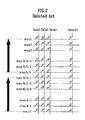
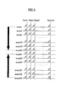
- FIG. 1 and FIG. 2 illustrate diagrams of general dual scan methods of passive matrix display panels, respectively.
- a display panel having "n (natural number as a multiple of '2')" scan lines is divided into an upper half and a lower half.
- the upper half includes 1 st to a (n/2) th scan lines and the lower half includes (n/2 + 1) th to n th scan lines.
- a sequential scan is carried out on the first scan line to the (n/2) th scan line.
- a sequential scan is carried out on the (n/2 + 1) th scan line to the n th scan line.
- a scan as shown in FIG. 2, can be carried out in a direction opposite to that of the display panel shown in FIG. 1.
- the scan is sequentially carried out on the scan lines of the upper half from the (n/2) th to the first scan lines while the other scan is sequentially carried out on the scan lines of the lower half from the n th to the (n/2 + 1) th scan lines.
- the present invention is directed to a dual scan method of a display panel that substantially obviates one or more problems due to limitations and disadvantages of the related art.
- An object of the present invention is to provide a dual scan method of a display panel enabling to remove strong light generated instantly from a central part of a display panel on driving the display panel by changing a scan order of scan lines.
- a dual scan method of a display panel having M data lines and N scan lines includes the steps of dividing the N scan lines into an upper half and a lower half and applying current to the scan lines of the upper half and the lower half respectively to scan, wherein the scan lines of the upper half and the scan lines of the lower half are sequentially scanned to be symmetrical to each other centering on a central axis of the display panel.
- the scan lines of the upper half and the scan lines of the lower half are sequentially scanned to be symmetrical to each other from outside to a center of the display panel.
- the scan lines of the upper half are scanned in a sequence from 1 st to (N/2) th scan lines and the scan lines of the lower half are scanned in a sequence from N th to (N/2 + 1) th scan lines, simultaneously.
- the scan lines of the upper half and the scan lines of the lower half are sequentially scanned to be symmetrical to each other from center to outside of the display panel.
- the scan lines of the upper half are scanned in a sequence from (N/2) th to 1 st scan lines and the scan lines of the lower half are scanned in a sequence from (N/2 + 1) th to N th scan lines, simultaneously.
- the scan lines of the upper half and the scan lines of the lower half are simultaneously scanned for one frame time.
- FIG. 1 and FIG. 2 illustrate diagrams of general dual scan methods of passive matrix display panels, respectively.
- FIG. 3 and FIG. 4 illustrate diagrams of dual scan methods of passive matrix display panels according to the present invention, respectively.
- FIG. 3 and FIG. 4 illustrate diagrams of dual scan methods of passive matrix display panels according to the present invention, respectively.
- Each of the display panels shown in FIG. 3 and FIG. 4 has a passive matrix structure of 120(column lines/data lines) * 160(row lines/scan lines).
- Each of the display panels of FIG. 3 and FIG. 4 carries out a dual scan on each eighty lines of upper and lower halves of scan lines.
- a display panel having one hundred sixty scan lines is divided into an upper half and a lower half.
- the upper half includes 1 st to 80 th scan lines and the lower half includes 81 st to 160 th scan lines.
- a scan line driving sequence of the above-constituted display panel according to the present invention is described as follows.
- a sequential scan is carried out on the scan lines (1 st to 80 th scan lines) of the upper half and the scan lines (81 st to 160 th scan lines) of the lower half to be symmetrical on a central axis of the panel.
- the scan is carried out so that the scan lines of the upper half and the other scan lines of the lower half are symmetrical to each other in a direction from outside to center of the panel.
- the scan is sequentially carried out on the scan lines of the upper half from the 1 st to 80 th scan lines while the other scan is sequentially carried out on the scan lines of the lower half from the 160 th to 81 st scan lines of the lower half.
- the scans are simultaneously carried out on the scan lines of the upper and lower halves for 1 frame time.
- the 1 st scan line of the upper half and the 160 th scan line of the lower half are simultaneously scanned.
- the 2 nd scan line of the upper half and the 159 th scan line of the lower half are simultaneously scanned.
- the 3 rd scan line of the upper half and the 158 th scan line of the lower half are simultaneously scanned.
- a 78 th scan time the 78 th scan line of the upper half and the 83 rd scan line of the lower half are simultaneously scanned. And, in a 79 th scan time, the 80 th scan line of the upper half and the 81 st scan line of the lower half are simultaneously scanned.
- the 80 th scan line of the upper half and the 81 st scan line of the lower half are simultaneously scanned to finish the scan for one frame.
- the scan is carried out in the above-explained same manner to make a corresponding pixel emit light.
- FIG. 4 illustrates another embodiment of the present invention.
- a display panel having one hundred sixty scan lines is divided into an upper half and a lower half.
- the upper half includes 1 st to 80 th scan lines and the lower half includes 81 st to 160 th scan lines.
- the scan lines (1 st to 80 th scan lines) of the upper half and the scan lines (81 st to 160 th scan lines) of the lower half are sequentially scanned to be symmetrical to each other on a central axis of the panel.
- the scan is carried out so that the scan lines of the upper half and the other scan lines of the lower half are symmetrical to each other in a direction from center to outside of the panel.
- the scan is sequentially carried out on the scan lines of the upper half from the 80 th to 1 st scan lines while the other scan is sequentially carried out on the scan lines of the lower half from the 81 st to 160 th scan lines of the lower half.
- the scans are simultaneously carried out on the scan lines of the upper and lower halves for 1 frame time.
- the 80 th scan line of the upper half and the 81 st scan line of the lower half are simultaneously scanned.
- the 1 st scan line of the upper half and the 160 th scan line of the lower half are simultaneously scanned to finish the scan for one frame.
- the scan is carried out in the above-explained same manner to make a corresponding pixel emit light.
- the dual scan method of the passive matrix display panel according to the present invention enables to eliminate the strong light generated instantly from the central part of the display panel by scanning the panel symmetrically on the central axis of the display panel.
Landscapes
- Engineering & Computer Science (AREA)
- Physics & Mathematics (AREA)
- Computer Hardware Design (AREA)
- General Physics & Mathematics (AREA)
- Theoretical Computer Science (AREA)
- Control Of Indicators Other Than Cathode Ray Tubes (AREA)
- Electroluminescent Light Sources (AREA)
- Control Of El Displays (AREA)
- Devices For Indicating Variable Information By Combining Individual Elements (AREA)
Abstract
Disclosed is a dual scan method of a display panel having M
data lines and N scan lines. The present invention includes the
steps of dividing the N scan lines into an upper half and a lower
half; and applying current to the scan lines of the upper half
and the lower half respectively to scan, wherein the scan lines
of the upper half and the scan lines of the lower half are
sequentially scanned to be symmetrical to each other centering on
a central axis of the display panel.
Description
- This application claims the benefit of the Korean Application No. P2002-18659 filed on April, 04 2002, which is hereby incorporated by reference.
- The present invention relates to a display panel, and more particularly, to a dual scan method of a display panel having a passive matrix structure.
- Recently, rapid progress has been made in a flat display panel field.
- Specifically, flat display panels including LCD (liquid crystal display) as a leading device appears in the markets to replace CRT (cathode ray tube) having been used most widely in the display field. Lately, the flat display panels including PDP (plasma display panel), VFD (visual fluorescent display), FED (field emission display), LED (light emitting diode), EL (electroluminescence), and the like have achieved great developments.
- Such a flat display panel requires a simple manufacturing process as well as high visibility and color sensation, thereby widening its application fields.
- Great attention is recently paid to an organic EL display as a flat display panel which occupies a small space as well as enables to have a wide screen size.
- The organic EL displays are classified into a passive matrix display and an active matrix display in accordance with panel structures.
- The passive matrix display has a structure that an organic EL material is located at each intersection between column and row lines.
- Hence, as an area of the passive matrix display increases, line resistance and capacitance increase to elongate an RC response time.
- The RC response time slows down the operation of the display as well as reduces brightness of the display.
- In order to decrease such a phenomenon, a dual scan method of scanning upper and lower parts of the display panel respectively is applied.
- Such a method elongates the light-emitting time of the display to increase the brightness but to reduce the influence of the resistance and capacitance.
- FIG. 1 and FIG. 2 illustrate diagrams of general dual scan methods of passive matrix display panels, respectively.
- Referring to FIG. 1, a display panel having "n (natural number as a multiple of '2')" scan lines is divided into an upper half and a lower half.
- In this case, the upper half includes 1st to a (n/2)th scan lines and the lower half includes (n/2 + 1)th to nth scan lines.
- For the scan lines of the upper half, a sequential scan is carried out on the first scan line to the (n/2)th scan line. Simultaneously, for the scan lines of the lower half, a sequential scan is carried out on the (n/2 + 1)th scan line to the nth scan line.
- On the other hand, a scan, as shown in FIG. 2, can be carried out in a direction opposite to that of the display panel shown in FIG. 1.
- Namely, the scan is sequentially carried out on the scan lines of the upper half from the (n/2)th to the first scan lines while the other scan is sequentially carried out on the scan lines of the lower half from the nth to the (n/2 + 1)th scan lines.
- Unfortunately, the above-explained dual scan methods have the problem that strong light is instantly generated from a central part of the panel as a boundary between the upper and lower halves.
- Accordingly, the present invention is directed to a dual scan method of a display panel that substantially obviates one or more problems due to limitations and disadvantages of the related art.
- An object of the present invention is to provide a dual scan method of a display panel enabling to remove strong light generated instantly from a central part of a display panel on driving the display panel by changing a scan order of scan lines.
- Additional advantages, objects, and features of the invention will be set forth in part in the description which follows and in part will become apparent to those having ordinary skill in the art upon examination of the following or may be learned from practice of the invention. The objectives and other advantages of the invention may be realized and attained by the structure particularly pointed out in the written description and claims hereof as well as the appended drawings.
- To achieve these objects and other advantages and in accordance with the purpose of the invention, as embodied and broadly described herein, a dual scan method of a display panel having M data lines and N scan lines according to the present invention includes the steps of dividing the N scan lines into an upper half and a lower half and applying current to the scan lines of the upper half and the lower half respectively to scan, wherein the scan lines of the upper half and the scan lines of the lower half are sequentially scanned to be symmetrical to each other centering on a central axis of the display panel.
- Preferably, the scan lines of the upper half and the scan lines of the lower half are sequentially scanned to be symmetrical to each other from outside to a center of the display panel.
- More preferably, the scan lines of the upper half are scanned in a sequence from 1st to (N/2)th scan lines and the scan lines of the lower half are scanned in a sequence from Nth to (N/2 + 1)th scan lines, simultaneously.
- Preferably, the scan lines of the upper half and the scan lines of the lower half are sequentially scanned to be symmetrical to each other from center to outside of the display panel.
- More preferably, the scan lines of the upper half are scanned in a sequence from (N/2)th to 1st scan lines and the scan lines of the lower half are scanned in a sequence from (N/2 + 1)th to Nth scan lines, simultaneously.
- Preferably, the scan lines of the upper half and the scan lines of the lower half are simultaneously scanned for one frame time.
- It is to be understood that both the foregoing general description and the following detailed description of the present invention are exemplary and explanatory and are intended to provide further explanation of the invention as claimed.
- The accompanying drawings, which are included to provide a further understanding of the invention and are incorporated in and constitute a part of this application, illustrate embodiment(s) of the invention and together with the description serve to explain the principle of the invention. In the drawings:
- FIG. 1 and FIG. 2 illustrate diagrams of general dual scan methods of passive matrix display panels, respectively; and
- FIG. 3 and FIG. 4 illustrate diagrams of dual scan methods of passive matrix display panels according to the present invention, respectively.
- Reference will now be made in detail to the preferred embodiments of the present invention, examples of which are illustrated in the accompanying drawings. Wherever possible, the same reference numbers will be used throughout the drawings to refer to the same or like parts.
- FIG. 3 and FIG. 4 illustrate diagrams of dual scan methods of passive matrix display panels according to the present invention, respectively.
- Each of the display panels shown in FIG. 3 and FIG. 4 has a passive matrix structure of 120(column lines/data lines) * 160(row lines/scan lines).
- Each of the display panels of FIG. 3 and FIG. 4 carries out a dual scan on each eighty lines of upper and lower halves of scan lines.
- Referring to FIG. 3, a display panel having one hundred sixty scan lines is divided into an upper half and a lower half.
- Namely, the upper half includes 1st to 80th scan lines and the lower half includes 81st to 160th scan lines.
- A scan line driving sequence of the above-constituted display panel according to the present invention is described as follows.
- Referring to FIG. 3, a sequential scan is carried out on the scan lines (1st to 80th scan lines) of the upper half and the scan lines (81st to 160th scan lines) of the lower half to be symmetrical on a central axis of the panel.
- Namely, the scan is carried out so that the scan lines of the upper half and the other scan lines of the lower half are symmetrical to each other in a direction from outside to center of the panel.
- The scan is sequentially carried out on the scan lines of the upper half from the 1st to 80th scan lines while the other scan is sequentially carried out on the scan lines of the lower half from the 160th to 81st scan lines of the lower half.
- Hence, the scans are simultaneously carried out on the scan lines of the upper and lower halves for 1 frame time.
- More specifically, in a 1st scan time, the 1st scan line of the upper half and the 160th scan line of the lower half are simultaneously scanned.
- Subsequently, in a 2nd scan time, the 2nd scan line of the upper half and the 159th scan line of the lower half are simultaneously scanned.
- Next, in a 3rd scan time, the 3rd scan line of the upper half and the 158th scan line of the lower half are simultaneously scanned.
- In the above-explained sequence manner, the respective scan lines are consecutively scanned.
- In a 78th scan time, the 78th scan line of the upper half and the 83rd scan line of the lower half are simultaneously scanned. And, in a 79th scan time, the 80th scan line of the upper half and the 81st scan line of the lower half are simultaneously scanned.
- Finally, in an 80th scan time, the 80th scan line of the upper half and the 81st scan line of the lower half are simultaneously scanned to finish the scan for one frame.
- And, in the subsequent frame, the scan is carried out in the above-explained same manner to make a corresponding pixel emit light.
- Using such a scan sequence can eliminate the instant light generated from a center of the panel.
- On the other hand, FIG. 4 illustrates another embodiment of the present invention.
- Referring to FIG. 4, a display panel having one hundred sixty scan lines is divided into an upper half and a lower half.
- Namely, the upper half includes 1st to 80th scan lines and the lower half includes 81st to 160th scan lines.
- The scan lines (1st to 80th scan lines) of the upper half and the scan lines (81st to 160th scan lines) of the lower half are sequentially scanned to be symmetrical to each other on a central axis of the panel.
- Namely, the scan is carried out so that the scan lines of the upper half and the other scan lines of the lower half are symmetrical to each other in a direction from center to outside of the panel.
- The scan is sequentially carried out on the scan lines of the upper half from the 80th to 1st scan lines while the other scan is sequentially carried out on the scan lines of the lower half from the 81st to 160th scan lines of the lower half.
- Hence, the scans are simultaneously carried out on the scan lines of the upper and lower halves for 1 frame time.
- More specifically, in a 1st scan time, the 80th scan line of the upper half and the 81st scan line of the lower half are simultaneously scanned.
- Subsequently, in a 2nd scan time, the 79th scan line of the upper half and the 82nd scan line of the lower half are simultaneously scanned.
- Next, in a 3rd scan time, the 78th scan line of the upper half and the 83rd scan line of the lower half are simultaneously scanned.
- In the above-explained sequence manner, the respective scan lines are consecutively scanned.
- In a 78th scan time, the 3rd scan line of the upper half and the 158th scan line of the lower half are simultaneously scanned. And, in a 79th scan time, the 2nd scan line of the upper half and the 159th scan line of the lower half are simultaneously scanned.
- Finally, in an 80th scan time, the 1st scan line of the upper half and the 160th scan line of the lower half are simultaneously scanned to finish the scan for one frame.
- And, in the subsequent frame, the scan is carried out in the above-explained same manner to make a corresponding pixel emit light.
- Using such a scan sequence can eliminate the instant light generated from a center of the panel.
- Accordingly, the dual scan method of the passive matrix display panel according to the present invention enables to eliminate the strong light generated instantly from the central part of the display panel by scanning the panel symmetrically on the central axis of the display panel.
- It will be apparent to those skilled in the art that various modifications and variations can be made in the present invention. Thus, it is intended that the present invention covers the modifications and variations of this invention provided they come within the scope of the appended claims and their equivalents.
Claims (6)
- A dual scan method of a display panel, the display panel having M data lines and N scan lines, the dual scan method comprising the steps of:dividing the N scan lines into an upper half and a lower half; andapplying current to the scan lines of the upper half and the lower half respectively to scan, wherein the scan lines of the upper half and the scan lines of the lower half are sequentially scanned to be symmetrical to each other centering on a central axis of the display panel.
- The dual scan method of claim 1, wherein the scan lines of the upper half and the scan lines of the lower half are sequentially scanned to be symmetrical to each other from outside to a center of the display panel.
- The dual scan method of claim 2, wherein the scan lines of the upper half are scanned in a sequence from 1st to (N/2)th scan lines and the scan lines of the lower half are scanned in a sequence from Nth to (N/2 + 1)th scan lines, simultaneously.
- The dual scan method of claim 1, wherein the scan lines of the upper half and the scan lines of the lower half are sequentially scanned to be symmetrical to each other from center to outside of the display panel.
- The dual scan method of claim 4, wherein the scan lines of the upper half are scanned in a sequence from (N/2)th to 1st scan lines and the scan lines of the lower half are scanned in a sequence from (N/2 + 1)th to Nth scan lines, simultaneously.
- The dual scan method of claim 1, wherein the scan lines of the upper half and the scan lines of the lower half are simultaneously scanned for one frame time.
Applications Claiming Priority (2)
| Application Number | Priority Date | Filing Date | Title |
|---|---|---|---|
| KR2002018659 | 2002-04-04 | ||
| KR1020020018659A KR20030080146A (en) | 2002-04-04 | 2002-04-04 | scan method of Organic Electroluminescence display device with passive matrix structure |
Publications (1)
| Publication Number | Publication Date |
|---|---|
| EP1353319A1 true EP1353319A1 (en) | 2003-10-15 |
Family
ID=28450127
Family Applications (1)
| Application Number | Title | Priority Date | Filing Date |
|---|---|---|---|
| EP03007770A Withdrawn EP1353319A1 (en) | 2002-04-04 | 2003-04-04 | Dual scan method of matrix display panel |
Country Status (5)
| Country | Link |
|---|---|
| US (1) | US20050073474A1 (en) |
| EP (1) | EP1353319A1 (en) |
| JP (1) | JP2003302937A (en) |
| KR (1) | KR20030080146A (en) |
| CN (1) | CN1450516A (en) |
Cited By (3)
| Publication number | Priority date | Publication date | Assignee | Title |
|---|---|---|---|---|
| EP1710778A1 (en) * | 2005-04-06 | 2006-10-11 | LG Electronics Inc. | Plasma display apparatus and driving method thereof |
| CN100385497C (en) * | 2004-07-10 | 2008-04-30 | 乐金电子(中国)研究开发中心有限公司 | Mobile communication terminal LCD driving device and method thereof |
| US7773053B2 (en) | 2004-07-30 | 2010-08-10 | Oki Semiconductor Co., Ltd. | Scanning method of display panel and a display unit |
Families Citing this family (17)
| Publication number | Priority date | Publication date | Assignee | Title |
|---|---|---|---|---|
| KR100515360B1 (en) | 2003-09-02 | 2005-09-15 | 삼성에스디아이 주식회사 | Plasma display panel and Driving method thereof |
| US7558884B2 (en) | 2004-05-03 | 2009-07-07 | Microsoft Corporation | Processing information received at an auxiliary computing device |
| US7511682B2 (en) | 2004-05-03 | 2009-03-31 | Microsoft Corporation | Context-aware auxiliary display platform and applications |
| JP2006023539A (en) | 2004-07-08 | 2006-01-26 | Tohoku Pioneer Corp | Self light emitting display panel and its driving method |
| KR100621020B1 (en) * | 2004-12-08 | 2006-09-19 | 엘지전자 주식회사 | Display unit control device and method of mobile terminal |
| US7728810B2 (en) * | 2005-11-28 | 2010-06-01 | Lg Display Co., Ltd. | Display device and method for driving the same |
| CN100446070C (en) * | 2006-02-10 | 2008-12-24 | 奇晶光电股份有限公司 | Driving method of dual-scanning display and related display device thereof |
| KR101128543B1 (en) * | 2006-06-09 | 2012-03-23 | 애플 인크. | Touch screen liquid crystal display |
| WO2011121654A1 (en) | 2010-03-31 | 2011-10-06 | パナソニック株式会社 | Method for driving stereoscopic display device, and stereoscopic display device |
| US20130021385A1 (en) * | 2011-07-22 | 2013-01-24 | Shenzhen China Star Optoelectronics Technology Co, Ltd. | Lcd device and black frame insertion method thereof |
| WO2014012247A1 (en) * | 2012-07-20 | 2014-01-23 | Shenzhen Yunyinggu Technology Co., Ltd. | Field sequential color display and driving method thereof |
| CN103208250B (en) * | 2013-03-26 | 2015-08-05 | 京东方科技集团股份有限公司 | A kind of driving circuit, driving method and display device |
| CN104575347A (en) * | 2013-10-10 | 2015-04-29 | 冠捷投资有限公司 | Flat panel display and driving circuit thereof |
| TWI505010B (en) * | 2013-11-12 | 2015-10-21 | E Ink Holdings Inc | Active device array substrate |
| US11538414B2 (en) | 2019-03-19 | 2022-12-27 | Sitronix Technology Corp. | Driving circuit of display panel |
| WO2021005772A1 (en) * | 2019-07-11 | 2021-01-14 | シャープNecディスプレイソリューションズ株式会社 | Multi-display device, display device, method for controlling multi-display device, and method for controlling display device |
| CN113205781A (en) * | 2020-02-03 | 2021-08-03 | 辉达公司 | Medium-to-outside technology for refreshing low-delay display |
Citations (5)
| Publication number | Priority date | Publication date | Assignee | Title |
|---|---|---|---|---|
| EP0441692A1 (en) * | 1990-02-06 | 1991-08-14 | Commissariat A L'energie Atomique | Control process for a matrix screen comprising two independent parts and device to carry it out |
| US5767831A (en) * | 1991-11-22 | 1998-06-16 | Sanyo Electric Co., Ltd. | Dot-matrix display for screen having multiple portions |
| JP2001045524A (en) * | 1999-01-26 | 2001-02-16 | Denso Corp | 3D display device |
| US20010003447A1 (en) * | 1999-12-08 | 2001-06-14 | Hiroyuki Murai | Liquid crystal display device |
| US6448952B1 (en) * | 1999-01-26 | 2002-09-10 | Denso Corporation | Stereoscopic image display device |
Family Cites Families (9)
| Publication number | Priority date | Publication date | Assignee | Title |
|---|---|---|---|---|
| JPH09130708A (en) * | 1995-10-31 | 1997-05-16 | Victor Co Of Japan Ltd | Liquid crystal image display device |
| JP3953544B2 (en) * | 1996-03-25 | 2007-08-08 | 株式会社デンソー | EL display device |
| JPH10133172A (en) * | 1996-10-30 | 1998-05-22 | Sharp Corp | Drive circuit for simple matrix display device |
| JPH1165486A (en) * | 1997-08-18 | 1999-03-05 | Nec Corp | Piasma display panel and its manufacture |
| JP2000259124A (en) * | 1999-03-05 | 2000-09-22 | Sanyo Electric Co Ltd | Electroluminescence display device |
| KR100341312B1 (en) * | 1999-10-27 | 2002-06-21 | 구자홍 | Method Of Driving Plasma Display Panel And Apparatus Thereof |
| KR100359021B1 (en) * | 2000-02-12 | 2002-10-31 | 엘지전자 주식회사 | Method of Driving Plasma Display Panel |
| KR100363677B1 (en) * | 2000-04-19 | 2002-12-05 | 엘지전자 주식회사 | Method of Driving Plasma Display Panel |
| KR100498282B1 (en) * | 2001-12-07 | 2005-07-01 | 엘지전자 주식회사 | Scan method for plat display device |
-
2002
- 2002-04-04 KR KR1020020018659A patent/KR20030080146A/en not_active Ceased
-
2003
- 2003-04-02 US US10/404,535 patent/US20050073474A1/en not_active Abandoned
- 2003-04-04 CN CN03128662A patent/CN1450516A/en active Pending
- 2003-04-04 EP EP03007770A patent/EP1353319A1/en not_active Withdrawn
- 2003-04-04 JP JP2003101331A patent/JP2003302937A/en active Pending
Patent Citations (5)
| Publication number | Priority date | Publication date | Assignee | Title |
|---|---|---|---|---|
| EP0441692A1 (en) * | 1990-02-06 | 1991-08-14 | Commissariat A L'energie Atomique | Control process for a matrix screen comprising two independent parts and device to carry it out |
| US5767831A (en) * | 1991-11-22 | 1998-06-16 | Sanyo Electric Co., Ltd. | Dot-matrix display for screen having multiple portions |
| JP2001045524A (en) * | 1999-01-26 | 2001-02-16 | Denso Corp | 3D display device |
| US6448952B1 (en) * | 1999-01-26 | 2002-09-10 | Denso Corporation | Stereoscopic image display device |
| US20010003447A1 (en) * | 1999-12-08 | 2001-06-14 | Hiroyuki Murai | Liquid crystal display device |
Non-Patent Citations (1)
| Title |
|---|
| PATENT ABSTRACTS OF JAPAN vol. 2000, no. 19 5 June 2001 (2001-06-05) * |
Cited By (4)
| Publication number | Priority date | Publication date | Assignee | Title |
|---|---|---|---|---|
| CN100385497C (en) * | 2004-07-10 | 2008-04-30 | 乐金电子(中国)研究开发中心有限公司 | Mobile communication terminal LCD driving device and method thereof |
| US7773053B2 (en) | 2004-07-30 | 2010-08-10 | Oki Semiconductor Co., Ltd. | Scanning method of display panel and a display unit |
| EP1710778A1 (en) * | 2005-04-06 | 2006-10-11 | LG Electronics Inc. | Plasma display apparatus and driving method thereof |
| US7768476B2 (en) | 2005-04-06 | 2010-08-03 | Lg Electronics Inc. | Plasma display apparatus and driving method thereof |
Also Published As
| Publication number | Publication date |
|---|---|
| KR20030080146A (en) | 2003-10-11 |
| JP2003302937A (en) | 2003-10-24 |
| US20050073474A1 (en) | 2005-04-07 |
| CN1450516A (en) | 2003-10-22 |
Similar Documents
| Publication | Publication Date | Title |
|---|---|---|
| EP1353319A1 (en) | Dual scan method of matrix display panel | |
| KR100394006B1 (en) | dual scan structure in current driving display element and production method of the same | |
| EP1391864A2 (en) | Flat display panel | |
| CN106782317B (en) | AMOLED display panel and its driving method and driving device | |
| CN106898296B (en) | Image processing circuit and display device with image processing circuit | |
| US20150228214A1 (en) | Display panel | |
| US20090135108A1 (en) | Sample-and-Hold Display with Impulse Backlight | |
| US6741037B2 (en) | Driving circuit of display for preventing electrostatic discharge | |
| US7142199B2 (en) | Matrix type-flat-panel display device having multi data lines and method for driving the same | |
| CN1418043A (en) | electroluminescent panel | |
| CN1855197A (en) | Display device and method of driving the same | |
| US7262748B2 (en) | Driving method for a plasma display panel | |
| KR100453165B1 (en) | Plasma display panel | |
| KR100680916B1 (en) | Multi-panel display and its driving method | |
| KR20030012302A (en) | driving circuit of current driving display element | |
| KR20030090408A (en) | method for interlacing scan of Organic Electroluminescence display device with passive matrix structure | |
| KR100352977B1 (en) | Field Emission Display and Driving Method thereof | |
| KR20030080148A (en) | method for random scan of Organic Electroluminescence display device with passive matrix structure | |
| US20220028322A1 (en) | Method for driving display device and driver | |
| KR100698701B1 (en) | Organic Light Emitting Display and Driving Method Thereof | |
| KR100608889B1 (en) | Organic electroluminescent display device and driving method thereof | |
| KR100610612B1 (en) | Driving method of organic electroluminescent display device | |
| KR100610618B1 (en) | Driving method of organic electroluminescent display device | |
| CN102074183B (en) | Method for driving field emission display | |
| JPS63163818A (en) | Reflected light reducing method for light emission type display device |
Legal Events
| Date | Code | Title | Description |
|---|---|---|---|
| PUAI | Public reference made under article 153(3) epc to a published international application that has entered the european phase |
Free format text: ORIGINAL CODE: 0009012 |
|
| AK | Designated contracting states |
Kind code of ref document: A1 Designated state(s): AT BE BG CH CY CZ DE DK EE ES FI FR GB GR HU IE IT LI LU MC NL PT RO SE SI SK TR |
|
| AX | Request for extension of the european patent |
Extension state: AL LT LV MK |
|
| 17P | Request for examination filed |
Effective date: 20040214 |
|
| 17Q | First examination report despatched |
Effective date: 20040326 |
|
| AKX | Designation fees paid |
Designated state(s): DE FR GB NL |
|
| STAA | Information on the status of an ep patent application or granted ep patent |
Free format text: STATUS: THE APPLICATION IS DEEMED TO BE WITHDRAWN |
|
| 18D | Application deemed to be withdrawn |
Effective date: 20061212 |