EP0441692A1 - Control process for a matrix screen comprising two independent parts and device to carry it out - Google Patents
Control process for a matrix screen comprising two independent parts and device to carry it out Download PDFInfo
- Publication number
- EP0441692A1 EP0441692A1 EP91400260A EP91400260A EP0441692A1 EP 0441692 A1 EP0441692 A1 EP 0441692A1 EP 91400260 A EP91400260 A EP 91400260A EP 91400260 A EP91400260 A EP 91400260A EP 0441692 A1 EP0441692 A1 EP 0441692A1
- Authority
- EP
- European Patent Office
- Prior art keywords
- lines
- line
- screen
- output
- information
- Prior art date
- Legal status (The legal status is an assumption and is not a legal conclusion. Google has not performed a legal analysis and makes no representation as to the accuracy of the status listed.)
- Granted
Links
Images


Classifications
-
- G—PHYSICS
- G09—EDUCATION; CRYPTOGRAPHY; DISPLAY; ADVERTISING; SEALS
- G09G—ARRANGEMENTS OR CIRCUITS FOR CONTROL OF INDICATING DEVICES USING STATIC MEANS TO PRESENT VARIABLE INFORMATION
- G09G3/00—Control arrangements or circuits, of interest only in connection with visual indicators other than cathode-ray tubes
- G09G3/20—Control arrangements or circuits, of interest only in connection with visual indicators other than cathode-ray tubes for presentation of an assembly of a number of characters, e.g. a page, by composing the assembly by combination of individual elements arranged in a matrix no fixed position being assigned to or needed to be assigned to the individual characters or partial characters
- G09G3/34—Control arrangements or circuits, of interest only in connection with visual indicators other than cathode-ray tubes for presentation of an assembly of a number of characters, e.g. a page, by composing the assembly by combination of individual elements arranged in a matrix no fixed position being assigned to or needed to be assigned to the individual characters or partial characters by control of light from an independent source
- G09G3/36—Control arrangements or circuits, of interest only in connection with visual indicators other than cathode-ray tubes for presentation of an assembly of a number of characters, e.g. a page, by composing the assembly by combination of individual elements arranged in a matrix no fixed position being assigned to or needed to be assigned to the individual characters or partial characters by control of light from an independent source using liquid crystals
- G09G3/3611—Control of matrices with row and column drivers
- G09G3/3622—Control of matrices with row and column drivers using a passive matrix
- G09G3/3644—Control of matrices with row and column drivers using a passive matrix with the matrix divided into sections
-
- G—PHYSICS
- G09—EDUCATION; CRYPTOGRAPHY; DISPLAY; ADVERTISING; SEALS
- G09G—ARRANGEMENTS OR CIRCUITS FOR CONTROL OF INDICATING DEVICES USING STATIC MEANS TO PRESENT VARIABLE INFORMATION
- G09G2310/00—Command of the display device
- G09G2310/02—Addressing, scanning or driving the display screen or processing steps related thereto
- G09G2310/0202—Addressing of scan or signal lines
- G09G2310/0221—Addressing of scan or signal lines with use of split matrices
-
- G—PHYSICS
- G09—EDUCATION; CRYPTOGRAPHY; DISPLAY; ADVERTISING; SEALS
- G09G—ARRANGEMENTS OR CIRCUITS FOR CONTROL OF INDICATING DEVICES USING STATIC MEANS TO PRESENT VARIABLE INFORMATION
- G09G2310/00—Command of the display device
- G09G2310/02—Addressing, scanning or driving the display screen or processing steps related thereto
- G09G2310/0224—Details of interlacing
-
- G—PHYSICS
- G09—EDUCATION; CRYPTOGRAPHY; DISPLAY; ADVERTISING; SEALS
- G09G—ARRANGEMENTS OR CIRCUITS FOR CONTROL OF INDICATING DEVICES USING STATIC MEANS TO PRESENT VARIABLE INFORMATION
- G09G2310/00—Command of the display device
- G09G2310/02—Addressing, scanning or driving the display screen or processing steps related thereto
- G09G2310/0264—Details of driving circuits
- G09G2310/0267—Details of drivers for scan electrodes, other than drivers for liquid crystal, plasma or OLED displays
-
- G—PHYSICS
- G09—EDUCATION; CRYPTOGRAPHY; DISPLAY; ADVERTISING; SEALS
- G09G—ARRANGEMENTS OR CIRCUITS FOR CONTROL OF INDICATING DEVICES USING STATIC MEANS TO PRESENT VARIABLE INFORMATION
- G09G2310/00—Command of the display device
- G09G2310/02—Addressing, scanning or driving the display screen or processing steps related thereto
- G09G2310/0264—Details of driving circuits
- G09G2310/0275—Details of drivers for data electrodes, other than drivers for liquid crystal, plasma or OLED displays, not related to handling digital grey scale data or to communication of data to the pixels by means of a current
-
- G—PHYSICS
- G09—EDUCATION; CRYPTOGRAPHY; DISPLAY; ADVERTISING; SEALS
- G09G—ARRANGEMENTS OR CIRCUITS FOR CONTROL OF INDICATING DEVICES USING STATIC MEANS TO PRESENT VARIABLE INFORMATION
- G09G3/00—Control arrangements or circuits, of interest only in connection with visual indicators other than cathode-ray tubes
- G09G3/20—Control arrangements or circuits, of interest only in connection with visual indicators other than cathode-ray tubes for presentation of an assembly of a number of characters, e.g. a page, by composing the assembly by combination of individual elements arranged in a matrix no fixed position being assigned to or needed to be assigned to the individual characters or partial characters
- G09G3/34—Control arrangements or circuits, of interest only in connection with visual indicators other than cathode-ray tubes for presentation of an assembly of a number of characters, e.g. a page, by composing the assembly by combination of individual elements arranged in a matrix no fixed position being assigned to or needed to be assigned to the individual characters or partial characters by control of light from an independent source
- G09G3/36—Control arrangements or circuits, of interest only in connection with visual indicators other than cathode-ray tubes for presentation of an assembly of a number of characters, e.g. a page, by composing the assembly by combination of individual elements arranged in a matrix no fixed position being assigned to or needed to be assigned to the individual characters or partial characters by control of light from an independent source using liquid crystals
- G09G3/3611—Control of matrices with row and column drivers
- G09G3/3674—Details of drivers for scan electrodes
- G09G3/3681—Details of drivers for scan electrodes suitable for passive matrices only
-
- G—PHYSICS
- G09—EDUCATION; CRYPTOGRAPHY; DISPLAY; ADVERTISING; SEALS
- G09G—ARRANGEMENTS OR CIRCUITS FOR CONTROL OF INDICATING DEVICES USING STATIC MEANS TO PRESENT VARIABLE INFORMATION
- G09G3/00—Control arrangements or circuits, of interest only in connection with visual indicators other than cathode-ray tubes
- G09G3/20—Control arrangements or circuits, of interest only in connection with visual indicators other than cathode-ray tubes for presentation of an assembly of a number of characters, e.g. a page, by composing the assembly by combination of individual elements arranged in a matrix no fixed position being assigned to or needed to be assigned to the individual characters or partial characters
- G09G3/34—Control arrangements or circuits, of interest only in connection with visual indicators other than cathode-ray tubes for presentation of an assembly of a number of characters, e.g. a page, by composing the assembly by combination of individual elements arranged in a matrix no fixed position being assigned to or needed to be assigned to the individual characters or partial characters by control of light from an independent source
- G09G3/36—Control arrangements or circuits, of interest only in connection with visual indicators other than cathode-ray tubes for presentation of an assembly of a number of characters, e.g. a page, by composing the assembly by combination of individual elements arranged in a matrix no fixed position being assigned to or needed to be assigned to the individual characters or partial characters by control of light from an independent source using liquid crystals
- G09G3/3611—Control of matrices with row and column drivers
- G09G3/3685—Details of drivers for data electrodes
- G09G3/3692—Details of drivers for data electrodes suitable for passive matrices only
Definitions
- the present invention relates to a method for controlling a matrix screen comprising two independent parts and a device for its implementation. It applies in particular to all matrix screens ordered in two independent parts and in particular to video screens (for example, liquid crystal screens or fluorescent microtip screens).
- a matrix screen of this type and in accordance with the prior art is described.
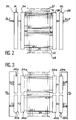
- Such a screen is made up of a first part 10 and a second part 12 which are independent but contiguous.
- Each part 10, 12 of the screen comprises N control lines crossed with M addressing columns.
- the lines of the first part 10 are successively selected simultaneously with the lines of the second part 12: the line 1 of the first part 10 with the line N + 1 of the second part 12, the line 2 with the line N + 2 and so on.
- the selection of the lines is carried out by a first register 6 for the first part 10 and a second register 8 for the second part 12.
- Signals DP for the register 6 and DS for the second register 8 provide the data relating to the line to be selected.
- a line scanning signal HL controls the selection of the lines.
- the registers 6 and 8 are respectively connected to means 9 and 11 amplifiers and impedance adapters for applying a determined potential to the selected lines.
- the information to be displayed is contained coded in binary form in a first and a second register 14, 16 which allow the addressing of the columns.
- the first and second registers 14, 16 are connected to decoders 21, 23 which allow the application to the columns of the screen of the potentials corresponding to the information to be displayed on the pixels of the selected lines.
- decoders 21, 23 which allow the application to the columns of the screen of the potentials corresponding to the information to be displayed on the pixels of the selected lines.
- the information to be displayed during the next selection is recorded in first and second buffer registers 18, 20.
- the first and second buffer registers 18, 20 are respectively connected to the first and second registers 14, 16 for transferring the information to be displayed.
- the information to be displayed is delivered in series, line after line.
- An intermediate memory 24 is therefore necessary: at a given instant, the information provided relates to only one line while two lines are displayed simultaneously (and also, it is necessary to fill in the two buffer registers 18, 20).
- This memory 24 therefore records the information to be displayed as it arrives and delivers to the buffer registers 18, 20 the information necessary for display. For this, it must be able to record the information to be displayed on all the lines of each part 10, 12 of the screen. It must therefore have a minimum capacity of 2N MK bits where: 2N is the number lines of the screen, M is the number of columns, and K is the number of bits necessary for coding the information to be displayed on a pixel.
- the present invention aims to reduce the size of this intermediate memory and thus reduce the cost of this type of screen.
- the invention recommends the simultaneous selection of a line of a first type of parity of the first part and of a line of a second type of parity of the second part. Then, all the lines of the first type of the first part and all the lines of the second type of the second part having been selected, a line of the second type of parity of the first part and a line of the first type of parity of the second part so as to select all the lines.
- this control method makes it possible to reduce the memory capacity to N / 2 MK bits, that is to say to reduce it by a factor of 4 compared to to that of the devices of the prior art.
- the present invention also relates to a device for implementing the method comprising for addressing the columns of the screen, a source capable of delivering on an output of information to display, a memory capable of recording the information to be displayed on the lines of one of the types of parity of the screen, connected to the output of the source, means for controlling the writing or reading of the memory, connected to said memory, means for generating write and read addresses connected to said memory, a first switching means connected on the one hand to the output of the source and on the other hand to an output of said memory, means for controlling the switching of the first switching means, connected to the first switching means, a second switching means connected on the one hand to the output of the source and on the other hand to the output of said memory , means for controlling the switching of the second switching means, connected to the second switching means, a first buffer register connected to an output of the first switching means, a second buffer register connected to an output of the second switching means, a first register connected as an input to an output of the first buffer register and capable of delivering information to be displayed on
- the memory is at least capable of simultaneously containing the information to be displayed on N / 2 lines of the screen.
- the memory once records information relating to the N lines of one of the types of parity on the screen, but at the same time as it performs these operations of writing information from the source, it transmits, during read operations, information to one or the other of the buffer registers of the device, so that at a given moment, the memory contains only N / 2.MK bits relating to the information of N / 2 lines .
- the means for writing and reading the memory is produced by a counter with two binary states having a counting input capable of receiving a pulse signal for synchronizing the delivery of the information to be displayed on a line and a second input capable of receiving a reset signal, this counter delivering on an output a pulse at each transition to its initial state and on another output connected to the memory a control signal L / E.
- the means for generating write and read addresses is produced by a counter with N / 2 binary states having a counting input connected to the output of the counter with two binary states delivering pulses to each transition to its initial state and a second input capable of receiving a reset signal, this counter delivering on an output a pulse at each transition to its initial state and on another output connected to the memory an address signal AD .
- the first and second means for controlling the switching of the first and second switching means are produced by a single circuit.
- said single circuit is a counter with two binary states having a counting input connected to the output of the counter with N / 2 binary states delivering on an output a pulse at each change to its initial state and a second input capable of receiving a reset signal, this counter delivering on an output connected to the first and second switching means a control signal HB.
- the device comprises: at least one register having a first input suitable for receiving a clock signal and a second input suitable for receiving a data signal.
- the device comprises: a first register having N stages for the selection of the N lines of the first type of parity of the first and second parts of the screen, and having a first input capable of receiving a clock signal and a second input capable of receiving a first data signal (DLI), a second register having N stages for the selection of the N lines of the second type of parity of the first and of the second parts of the screen and having a first input capable of receiving the clock signal and a second input capable of receiving a second data signal (DLP).
- a first register having N stages for the selection of the N lines of the first type of parity of the first and second parts of the screen, and having a first input capable of receiving a clock signal and a second input capable of receiving a second data signal (DLP).
- DLP second data signal
- Figures 2, 3, 4 and 6 schematically represent different variants of a circuit for the selection of a matrix screen having two parts 10, 12 independent but contiguous so as to ensure the continuity of the rows and columns.
- the screen can be of the liquid crystal or fluorescent microtip type.
- Each part 10, 12 comprises an even number N of lines; for the first part 10, these lines are numbered from 1 to N; for the second part 12, they are numbered from N + 1 to 2N.
- the lines of the screen are therefore divided into odd lines and successive pairs.
- Each part of the screen further comprises M columns. Screen pixels are formed at each crossing of rows and columns.
- each line of a first type of parity of the first part 10 of the screen is selected simultaneously with a line of a second type of parity of the second part 12
- each line of the second type of parity of the first part 10 is selected simultaneously with a line of the first type of parity of the second part 12.
- FIG. 2 schematically represents a matrix screen comprising two contiguous parts 10, 12 provided with a line selection circuit according to the invention.
- the selection circuit comprises two registers 26, 28 with N stages respectively supplied with data signals DLI, DLP relating to the odd and even lines to be selected and delivered by a control circuit not shown.
- the register 26 is connected to means 34 of impedance amplifiers and adapters, themselves connected to the odd lines of the first part 10 and the second part 12.
- the register 28 is connected to means 38 impedance amplifiers and adapters, themselves connected to the even lines of the first part 10 and the second part 12.
- the signals DLI, DLP, respectively applied to the registers 26, 28 indicate the lines to be selected during the first selection.
- the lines to be selected at the start of the frame time are lines 1 and N + 2
- the signals DLI and DLP correspond respectively to binary elements of which only the first binary element is non-zero for DLI and of which only the N / 2 + 1 binary element corresponding to the line N + 2 is non-zero for DLP.
- the following selections are obtained by shifting the signals contained in the registers by applying clock pulses HL to inputs of registers 26 and 28.
- the register 26 selects, one after the other, the odd lines of the first part 10.
- the register 28 selects, one after the other, the even lines of the second part 12.
- each odd line of the first part 10 is selected simultaneously with the selection of an even line of the second part 12 to which it is paired.
- the line numbered 1 is selected simultaneously with the line numbered N + 2 and so on until the last odd numbered line N-1 of the first part 10 selected simultaneously with the line numbered 2N of the second part 12.
- the register 28 selects, one after the other, the even lines of the first part 10.
- the register 26 selects, one after the other, the odd lines of the second part 12.
- each even line of the first part 10 is selected simultaneously when selecting an odd line from the second part to which it is paired.
- the line numbered 2 is selected simultaneously with the line numbered N + 1 and so on until the last even line of the first part 10 numbered N selected simultaneously with the line numbered 2N-1 of the second part 12.
- FIG. 3 schematically represents an alternative embodiment of a selection circuit. This variant allows the selection of the successive odd (respectively odd) lines of the first part 10 simultaneously with the successive even (odd) lines of the second part 12 with which they are paired.
- the selection circuit further comprises four registers 26a, 28a, 30a, 32a with N / 2 stages connected as above to means 34a, 38a, 36a, 40a, amplifiers and impedance adapters.
- the four registers are not interconnected but an identical clock signal HL and applied to an input of each of the registers controls the selection of a line.
- data signals DLI1, DLP1, DLI2, DLP2 delivered by a control circuit not shown are respectively applied to the registers 26a, 28a, 30a, 32a.
- these data signals introduce into the stages of the corresponding registers signals corresponding to binary elements of which only the stage corresponding to a line to be selected contains a non-zero binary element.
- the signals contained in the registers undergo an offset at each clock pulse so as to select the lines to be.
- registers 26a and 32a (containing a non-zero binary element) each select a line while registers 28a and 30a (containing only zero binary elements) do not select one; the situation is reversed during the next half-frame.
- FIG. 4 schematically represents another variant of a selection circuit according to the invention.
- the latter consists of two registers 42, 44 with N stages respectively connected to means 46, 48 amplifiers and impedance adapters.
- the amplifier and impedance adapter means 46 is connected to the lines of the first part 10; the means 48 amplifier and impedance adapter is connected to the lines of the second part 12.
- Data signals DL1 and DL2 delivered by a control circuit not shown, allow the selection of the lines of each part.
- HL clock pulses supplied to inputs of registers 42 and 44 control the shifts of the information contained in registers 42 and 44 and therefore each new selection of a pair of lines.
- This type of selection circuit requires clock pulses having an asymmetric timing diagram.
- the stages of the registers supplied by the signals DL1 and DL2 allow, during a first half of the duration of a frame, the simultaneous selection of an odd line of the first part 10 with an even line of the second part 12 During the second half of the duration of a frame, they allow the simultaneous selection of a line pair of the first part 10 with an odd line of the second part 12. During each half-frame, the lines which should not be displayed are selected for too short a time to be effective.
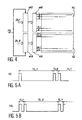
- FIG. 5A we see the timing diagram of the clock pulses HL for the selection of the odd lines of the first part 10 and the even lines of the second part used during the first half of a frame time.
- Two different periods TL1 and TL2 are used for the selection of the odd and even lines of the first part 10 (and of the even and odd lines to which they are paired).
- the duration of a period TL1 separating two clock pulses during the selection of an odd line of the first part 10 (or of an even line of the second part) is substantially equal to the usual duration of selection of a line.
- the duration of a period TL2 separating two clock pulses during the selection of an even line of the first part (or of an odd line of the second part) is much less than the usual duration of selection d 'a line. In this way, the even lines of part 10 and the odd lines of part 12 are selected for too short a time for a display to be initiated on these lines.
- FIG. 5B shows the chronogram of the clock pulses HL for the selection of the even lines of the first part 10 and of the paired odd lines of the second part 12 used during the second half of a frame time.
- TL1 has a duration much less than the usual duration for selecting a line while TL2 has a duration substantially equal to the usual duration for selecting a line. In this way, the selection of the lines which should not support a display is carried out only for too short a time for a display to be initiated and their selection is of no consequence.
- FIG. 6 schematically represents another alternative embodiment of a line selection circuit according to the invention.
- This circuit uses only a register 50 to 2N stages connected to an amplifier means 52 and impedance adapter itself connected to the lines of the two parts 10, 12 of the screen.
- the signals DL correspond to the set of signals DL1 and DL2 in FIG. 4.
- the register 50 therefore contains two non-zero binary elements.
- the clock pulses H delivered on an entry of the register present an asymmetric chronogram in a manner analogous to those of FIGS. 5A and 5B.
- the pulses corresponding to the timing diagram of FIG. 5A are applied during a first half-frame and the pulses corresponding to the timing diagram of FIG. 5B are applied during the following half-frame.
- FIG. 7 schematically represents a circuit for addressing the columns of the screen according to the invention.
- a source 22 delivers information coded in binary in an order relating to the successive lines of the screen. This source also delivers TL clock pulses in synchronism with the delivery of information. to be displayed on one line of the screen and TT frame pulses. Each piece of information to be displayed on a pixel of the screen is binary coded by a number of K bits.
- the output of the source delivering the information to be displayed is connected to an input of a memory 62 of capacity at least capable of simultaneously containing the information to be displayed on N / 2 lines of the screen, to an input of a circuit 64 for addressing the columns of the first part of the screen and to an input of a circuit 66 for addressing the columns of the second part of the screen.
- the circuit 64 comprises: a switching means 68 of the multiplexer type connected on the one hand to the source 22 and on the other hand to an output of the memory 62, a buffer register 70 connected to an output of the switching means 68, a register 72 connected to an output of the buffer register 70 and a decoder 21 connected by an input to the register 72 and at the output to the columns of the first part 10 of the screen.
- the circuit 66 comprises, connected in a similar manner to the preceding circuit, a switching means 74 of the multiplexer type, a buffer register 76, a register 78 and a decoder 23 connected to the columns of the second part 12 of the screen.
- the decoders 21 and 23 carry out an adaptation between the information in binary form contained in the registers 72 and 78 and the information to be applied to the columns.
- the addressing circuit also comprises, a means 80 for writing and reading from the memory and delivering on an output connected to an input of the memory 62 a L / E signal for writing or of reading.
- This means 80 can be produced by a counter with two binary states having first and second data inputs connected to the outputs of the source 22 delivering the clock pulses and the frame pulses, the latter carrying out a reset of the counter. 80.
- the counter From the reset to zero, following the first clock pulse TL, the counter delivers for example a read signal in memory 62; following the second clock pulse, the counter delivers a write signal to memory 62.
- the counter operates in this way for successive clock pulses until the new reset to zero during a frame pulse.
- the memory only records the information relating to lines of a single type of parity.
- the memory records only the information to be displayed on the even lines of the screen.
- the latter transmits the information relating to a selected even line by means of switches 68 or 74 depending on whether the selected line is included in part 10 or 12 of the screen.
- this counter 80 delivers pulses IC1 on an output each time it regains its initial state, that is to say every two clock pulses.
- the addressing circuit further comprises means 82 for generating write and read addresses connected by an output to an input of memory 62.
- This means 82 can be implemented by a counter with N / 2 binary states having a counting input connected to an output of the counter 80 with two binary states for receiving the pulses IC1. It also has a second input connected to the output of the source 22 delivering the frame pulses which allow resetting of the counter 82.
- the means 82 supplies the memory with a signal AD designating the addresses of the writes and readings in memory 62.
- Each address is composed by a word of L bits with L integer and respecting the condition:
- the signal AD designates a particular address common to the reading of a line from one part of the screen and the writing of a line from the other part of the screen.
- the addresses of reading and writing of these lines correspond respectively to 1, 2, ... N / 2 coded in binary.
- Each AD address being maintained during a read pulse and a write pulse, the information of the corresponding line stored in the memory at the address AD is read and then replaced by information corresponding to a line of the other part of the screen.
- These two lines are lines of the same order in each part, i.e. 2 and N + 2 or N + 2 and 2, 4 and N + 4 or N + 4 and 4 ... N and 2N or 2N and N.
- the counter with N / 2 binary states delivers an IC2 pulse on an output.
- the addressing circuit finally comprises means for controlling the switches of the switching means 68, 74. These means are produced by a counter 84 with two binary states.
- This counter 84 has a counting input connected to an output of the counter with N / 2 binary states for the reception of the pulses IC2. It also has a second input connected to the output of the source 22 delivering frame pulses which trigger its reset.
- the counter 84 delivers a signal HB whose binary value determines whether the multiplexers 68 and 74 deliver to the buffer registers 70 and 76 the information coming directly from the source 22 and relating to the odd lines or coming from the memory 62 and relating to the even lines .
- the multiplexer 68 delivers on its output the information coming from the source 22, while the multiplexer 74 delivers on its output the information coming from the memory 62.
- the multiplexer 68 delivers on its outputs information from memory 62, while multiplexer 74 delivers information from source 22 at its output.
- the selection by the circuit for selecting the lines to be displayed begins synchronously with the delivery by the source 22 of the information to be displayed on an odd line of the screen. This synchronism is obtained by virtue of the clock pulses TL and of frame TT which are transformed or not to form the clock pulses triggering the register or registers of the selection circuit.
- the information to be displayed on the even lines of the screen is recorded in the memory 62.
- the registers 72 and 78 record the information contained in the buffer registers 70 and 76 respectively. This information decoded by the decoders 21 and 23 is displayed on the selected lines of the first and second parts of the screen.
- the buffer registers 70 and 76 then record the information to be displayed during the next selection.
- This information comes either directly from the source 22 or from the memory 62 via the multiplexers 68 and 74 controlled by the signal HB. There is therefore constantly a time lag between the supply of the information by the source 22 and its display. This offset is equal to half a frame time for the information to be displayed on an even line while it is only equal to the time for selecting a line for the information to be displayed on an odd line.
- the first frame allows the initialization of counters, registers and filling the memory with the information to be displayed on half of the even lines of the next frame.
Landscapes
- Engineering & Computer Science (AREA)
- Physics & Mathematics (AREA)
- Computer Hardware Design (AREA)
- General Physics & Mathematics (AREA)
- Theoretical Computer Science (AREA)
- Chemical & Material Sciences (AREA)
- Crystallography & Structural Chemistry (AREA)
- Control Of Indicators Other Than Cathode Ray Tubes (AREA)
- Liquid Crystal Display Device Control (AREA)
- Controls And Circuits For Display Device (AREA)
Abstract
Description
La présente invention a pour objet un procédé de commande d'un écran matriciel comportant deux parties indépendantes et un dispositif pour sa mise en oeuvre. Elle s'applique notamment à tous les écrans matriciels commandés en deux parties indépendantes et en particulier aux écrans vidéo (par exemple, écrans à cristaux liquides ou écrans fluorescents à micropointes).The present invention relates to a method for controlling a matrix screen comprising two independent parts and a device for its implementation. It applies in particular to all matrix screens ordered in two independent parts and in particular to video screens (for example, liquid crystal screens or fluorescent microtip screens).
En référence à la figure 1, on décrit un écran matriciel de ce type et conforme à l'art antérieur. Un tel écran se compose d'une première partie 10 et d'une seconde partie 12 indépendantes mais jointives. Chaque partie 10, 12 de l'écran comporte N lignes de commande croisées à M colonnes d'adressage.With reference to FIG. 1, a matrix screen of this type and in accordance with the prior art is described. Such a screen is made up of a
Pour l'affichage, les lignes de la première partie 10 sont successivement sélectionnées simultanément aux lignes de la seconde partie 12 : la ligne 1 de la première partie 10 avec la ligne N+1 de la seconde partie 12, la ligne 2 avec la ligne N+2 et ainsi de suite.For the display, the lines of the
La sélection des lignes est effectuée par un premier registre 6 pour la première partie 10 et un second registre 8 pour la seconde partie 12. Des signaux DP pour le registre 6 et DS pour le second registre 8 fournissent les données concernant la ligne à sélectionner. Un signal HL de balayage des lignes commande la sélection des lignes.The selection of the lines is carried out by a first register 6 for the
Les registres 6 et 8 sont respectivement connectés à des moyens 9 et 11 amplificateurs et adaptateurs d'impédance permettant d'appliquer sur les lignes sélectionnées un potentiel déterminé.The
A chaque sélection d'une ligne d'une partie simultanément à une ligne de l'autre partie, les informations à afficher sont contenues codées sous forme binaire dans un premier et un second registres 14, 16 qui permettent l'adressage des colonnes. Les premier et second registres 14, 16 sont connectés à des décodeurs 21, 23 qui permettent l'application sur les colonnes de l'écran des potentiels correspondant aux informations à afficher sur les pixels des lignes sélectionnées. Pendant la durée de cette sélection, les informations à afficher lors de la sélection suivante sont enregistrées dans un premier et un second registres-tampons 18, 20.With each selection of a line of a part simultaneously with a line of the other part, the information to be displayed is contained coded in binary form in a first and a
Les premier et second registres-tampons 18, 20 sont respectivement reliés aux premier et second registres 14, 16 pour le transfert des informations à afficher.The first and
Pour un signal V du type vidéo fourni par une source 22, les informations à afficher sont délivrées en série, ligne après ligne. Une mémoire intermédiaire 24 est donc nécessaire : à un instant donné, les informations fournies ne concernent qu'une seule ligne alors que deux lignes sont affichées simultanément (et aussi, il est nécessaire de remplir les deux registres-tampons 18, 20).For a signal V of the video type supplied by a
Cette mémoire 24 enregistre donc les informations à afficher au fur et à mesure de leur arrivée et délivre aux registres-tampon 18, 20 les informations nécessaires à l'affichage. Pour cela, elle doit être capable d'enregistrer les informations à afficher sur toutes les lignes de chaque partie 10, 12 de l'écran. Elle doit donc présenter une capacité minimale de 2N M K bits où : 2N est le nombre de lignes de l'écran, M est le nombre de colonnes, et K est le nombre de bits nécessaire au codage des informations à afficher sur un pixel.This
L'importante capacité de la mémoire constitue un inconvénient grave de ce type d'écran connu. En effet, le coût du dispositif croît avec la taille de celle-ci.The large memory capacity is a serious drawback of this type of known screen. Indeed, the cost of the device increases with the size thereof.
La présente invention a pour but de réduire la taille de cette mémoire intermédiaire et ainsi de diminuer le coût de ce type d'écran.The present invention aims to reduce the size of this intermediate memory and thus reduce the cost of this type of screen.
Pour cela, les lignes successives de l'écran étant réparties en lignes paires et impaires successives, l'invention préconise la sélection simultanée d'une ligne d'un premier type de parité de la première partie et d'une ligne d'un second type de parité de la seconde partie. Puis, toutes les lignes du premier type de la première partie et toutes les lignes du second type de la seconde partie ayant été sélectionnées, on sélectionne simultanément une ligne du second type de parité de la première partie et une ligne du premier type de parité de la seconde partie de façon à sélectionner l'ensemble des lignes.For this, the successive lines of the screen being distributed in successive even and odd lines, the invention recommends the simultaneous selection of a line of a first type of parity of the first part and of a line of a second type of parity of the second part. Then, all the lines of the first type of the first part and all the lines of the second type of the second part having been selected, a line of the second type of parity of the first part and a line of the first type of parity of the second part so as to select all the lines.
Comme on va le voir plus en détail dans la description qui suit, ce procédé de commande permet de réduire la capacité de la mémoire à N/2 M K bits, c'est-à-dire de la réduire d'un facteur 4 par rapport à celle des dispositifs de l'art antérieur.As will be seen in more detail in the description which follows, this control method makes it possible to reduce the memory capacity to N / 2 MK bits, that is to say to reduce it by a factor of 4 compared to to that of the devices of the prior art.
De façon plus précise, l'invention concerne un procédé de commande d'un écran matriciel composé d'une première partie et d'une seconde partie comportant chacune un nombre N pair de lignes, les lignes de chacune des parties étant réparties en lignes d'un premier type de parité et lignes d'un second type de parité successives, caractérisé en ce qu'il consiste à :
pour chaque trame de l'écran,
- A) sélectionner, les unes après les autres, les lignes du premier type de parité successives de la première partie ;
sélectionner, les unes après les autres, les lignes du second type de parité successives de la seconde partie,
chaque ligne du premier type de la première partie étant sélectionnée simultanément à une ligne du second type de la seconde partie à laquelle elle est appariée, - B) puis, sélectionner, les unes après les autres, les lignes du second type de parité successives de la première partie,
sélectionner, les unes après les autres, les lignes du premier type de parité successives de la seconde partie,
chaque ligne du second type de la première partie étant sélectionnée simultanément à une ligne du premier type de la seconde partie à laquelle elle est appariée, - C) pour chaque ligne sélectionnée, afficher des informations devant l'être.
On entend par lignes d'un premier type de parité les lignes impaires et par lignes d'un second type de parité les lignes paires ou l'inverse. Dans le cas où le nombre total de lignes de l'écran est impair, pour avoir deux parties comportant un nombre N identique de lignes, on utilise pour une des parties une ligne fictive qui n'est pas affichée mais qui est prise en compte par l'électronique de l'écran au niveau temporel. De même, lorsque la moitié du nombre total de lignes est impaire, on ajoute pour avoir N pair une ligne fictive à chaque partie. On peut donc avoir jusqu'à trois lignes fictives pour un écran.
Selon un mode préféré de réalisation du procédé, lesdites informations à afficher étant délivrées par une source à un rythme régulier et dans un ordre relatif aux lignes successives de l'écran, - D) au fur et à mesure de leur délivrance, on enregistre dans une mémoire les informations à afficher sur les lignes d'un des types de parité de l'écran,
- E) parallèlement à chaque sélection d'une ligne de la première partie appariée à une ligne de la seconde partie, chaque sélection débutant de manière synchrone avec la délivrance par la source des informations à afficher sur une ligne de l'autre type de parité de l'écran,
- a) on enregistre dans un premier registre à partir d'un premier registre-tampon les informations à afficher sur ladite ligne sélectionnée de la première partie,
- b) on enregistre dans un second registre à partir d'un second registre-tampon les informations à afficher sur ladite ligne sélectionnée de la seconde partie,
- c) on enregistre les informations délivrées par la source et à afficher sur la ligne dudit autre type de parité de la sélection suivante dans le registre-tampon qui est associé à ladite ligne,
- d) on transfère à partir de la mémoire les informations à afficher sur la ligne de parité définie en D) de la sélection suivante dans le registre-tampon qui est associé à ladite ligne.
for each screen frame,
- A) select, one after the other, the lines of the first successive type of parity of the first part;
select, one after the other, the lines of the second successive type of parity of the second part,
each line of the first type of the first part being selected simultaneously with a line of the second type of the second part to which it is paired, - B) then select, one after the other, the lines of the second successive type of parity of the first part,
select, one after the other, the lines of the first successive type of parity of the second part,
each line of the second type of the first part being selected simultaneously with a line of the first type of the second part to which it is paired, - C) for each selected line, display information that must be displayed.
The lines of a first type of parity are understood to mean the odd lines and the lines of a second type of parity to mean the even lines or the reverse. In the case where the total number of lines of the screen is odd, to have two parts comprising an identical number N of lines, one uses for one of the parts a fictitious line which is not displayed but which is taken into account by screen electronics at the time level. Similarly, when half of the total number of lines is odd, we add to have N even a fictitious line to each part. We can therefore have up to three fictitious lines for a screen.
According to a preferred embodiment of the method, said information to be displayed being delivered by a source at a regular rate and in an order relating to the successive lines of the screen, - D) as and when they are delivered, the information to be displayed on the lines of one of the parity types of the screen is recorded in a memory,
- E) parallel to each selection of a line of the first part paired with a line of the second part, each selection starting synchronously with the delivery by the source of the information to be displayed on a line of the other type of parity the screen,
- a) the information to be displayed on said selected line of the first part is recorded in a first register from a first buffer register,
- b) the information to be displayed on said selected line of the second part is recorded in a second register from a second buffer register,
- c) the information delivered by the source is recorded and to be displayed on the line of said other type of parity of the following selection in the buffer register which is associated with said line,
- d) the information to be displayed on the parity line defined in D) of the following selection is transferred from the memory into the buffer register which is associated with said line.
La présente invention concerne aussi un dispositif pour la mise en oeuvre du procédé comprenant pour adresser les colonnes de l'écran,
une source apte à délivrer sur une sortie des informations à afficher,
une mémoire apte à enregister les informations à afficher sur les lignes d'un des types de parité de l'écran, connectée à la sortie de la source,
un moyen pour commander l'écriture ou la lecture de la mémoire, connecté à ladite mémoire,
un moyen pour engendrer des adresses d'écriture et de lecture connecté à ladite mémoire,
un premier moyen d'aiguillage connecté d'une part à la sortie de la source et d'autre part à une sortie de ladite mémoire,
un moyen pour commander l'aiguillage du premier moyen d'aiguillage, connecté au premier moyen d'aiguillage, un second moyen d'aiguillage connecté d'une part à la sortie de la source et d'autre part à la sortie de ladite mémoire,
un moyen pour commander l'aiguillage du second moyen d'aiguillage, connecté au second moyen d'aiguillage, un premier registre-tampon connecté à une sortie du premier moyen d'aiguillage,
un second registre-tampon connecté à une sortie du second moyen d'aiguillage,
un premier registre connecté en entrée à une sortie du premier registre-tampon et apte à délivrer des informations à afficher sur une ligne sélectionnée de la première partie de l'écran,
un second registre connecté en entrée à une sortie du second registre-tampon et apte à délivrer des informations à afficher sur une ligne sélectionnée de la seconde partie de l'écran.The present invention also relates to a device for implementing the method comprising for addressing the columns of the screen,
a source capable of delivering on an output of information to display,
a memory capable of recording the information to be displayed on the lines of one of the types of parity of the screen, connected to the output of the source,
means for controlling the writing or reading of the memory, connected to said memory,
means for generating write and read addresses connected to said memory,
a first switching means connected on the one hand to the output of the source and on the other hand to an output of said memory,
means for controlling the switching of the first switching means, connected to the first switching means, a second switching means connected on the one hand to the output of the source and on the other hand to the output of said memory ,
means for controlling the switching of the second switching means, connected to the second switching means, a first buffer register connected to an output of the first switching means,
a second buffer register connected to an output of the second switching means,
a first register connected as an input to an output of the first buffer register and capable of delivering information to be displayed on a selected line of the first part of the screen,
a second register connected as an input to an output of the second buffer register and capable of delivering information to be displayed on a selected line of the second part of the screen.
De manière avantageuse, la mémoire est au moins apte à contenir simultanément les informations à afficher sur N/2 lignes de l'écran.Advantageously, the memory is at least capable of simultaneously containing the information to be displayed on N / 2 lines of the screen.
En effet, au cours d'une trame la mémoire enregistre une fois l'information relative aux N lignes d'un des types de parité de l'écran, mais en même temps qu'elle effectue ces opérations d'écriture des informations en provenance de la source, elle transmet, au cours d'opérations de lecture, des informations à l'un ou à l'autre des registres-tampons du dispositif, de sorte qu'à un moment donné, la mémoire ne contient que N/2.M.K bits relatifs aux informations de N/2 lignes.Indeed, during a frame the memory once records information relating to the N lines of one of the types of parity on the screen, but at the same time as it performs these operations of writing information from the source, it transmits, during read operations, information to one or the other of the buffer registers of the device, so that at a given moment, the memory contains only N / 2.MK bits relating to the information of N / 2 lines .
Selon un mode de réalisation particulier, le moyen de commande d'écriture et de lecture de la mémoire est réalisé par un compteur à deux états binaires présentant une entrée de comptage apte à recevoir un signal impulsionnel de synchronisation de la délivrance des informations à afficher sur une ligne et une deuxième entrée apte à recevoir un signal de remise à zéro, ce compteur délivrant sur une sortie une impulsion à chaque passage à son état initial et sur une autre sortie connectée à la mémoire un signal de commande L/E.According to a particular embodiment, the means for writing and reading the memory is produced by a counter with two binary states having a counting input capable of receiving a pulse signal for synchronizing the delivery of the information to be displayed on a line and a second input capable of receiving a reset signal, this counter delivering on an output a pulse at each transition to its initial state and on another output connected to the memory a control signal L / E.
Dans ce mode de réalisation, avantageusement, le moyen pour engendrer des adresses d'écriture et de lecture est réalisé par un compteur à N/2 états binaires présentant une entrée de comptage connectée à la sortie du compteur à deux états binaires délivrant des impulsions à chaque passage à son état initial et une deuxième entrée apte à recevoir un signal de remise à zéro, ce compteur délivrant sur une sortie une impulsion à chaque passage à son état initial et sur une autre sortie connectée à la mémoire un signal d'adresse AD.In this embodiment, advantageously, the means for generating write and read addresses is produced by a counter with N / 2 binary states having a counting input connected to the output of the counter with two binary states delivering pulses to each transition to its initial state and a second input capable of receiving a reset signal, this counter delivering on an output a pulse at each transition to its initial state and on another output connected to the memory an address signal AD .
Selon un mode de réalisation préféré, les premier et second moyens pour commander l'aiguillage des premier et second moyens d'aiguillage sont réalisés par un circuit unique.According to a preferred embodiment, the first and second means for controlling the switching of the first and second switching means are produced by a single circuit.
Avantageusement, ledit circuit unique est un compteur à deux états binaires présentant une entrée de comptage connectée à la sortie du compteur à N/2 états binaires délivrant sur une sortie une impulsion à chaque passage à son état initial et une deuxième entrée apte à recevoir un signal de remise à zéro, ce compteur délivrant sur une sortie connectée aux premier et second moyens d'aiguillage un signal de commande HB.Advantageously, said single circuit is a counter with two binary states having a counting input connected to the output of the counter with N / 2 binary states delivering on an output a pulse at each change to its initial state and a second input capable of receiving a reset signal, this counter delivering on an output connected to the first and second switching means a control signal HB.
Selon un mode de réalisation avantageux pour sélectionner les lignes de l'écran, le dispositif comprend :
au moins un registre présentant une première entrée apte à recevoir un signal d'horloge et une seconde entrée apte à recevoir un signal de donnée.According to an advantageous embodiment for selecting the lines of the screen, the device comprises:
at least one register having a first input suitable for receiving a clock signal and a second input suitable for receiving a data signal.
Selon un mode particulier de réalisation, le dispositif comprend :
un premier registre présentant N étages pour la sélection des N lignes du premier type de parité de la première et la seconde parties de l'écran, et ayant une première entrée apte à recevoir un signal d'horloge et une seconde entrée apte à recevoir un premier signal de donnée (DLI),
un second registre présentant N étages pour la sélection des N lignes du second type de parité de la première et de la seconde parties de l'écran et ayant une première entrée apte à recevoir le signal d'horloge et une seconde entrée apte à recevoir un second signal de donnée (DLP).According to a particular embodiment, the device comprises:
a first register having N stages for the selection of the N lines of the first type of parity of the first and second parts of the screen, and having a first input capable of receiving a clock signal and a second input capable of receiving a first data signal (DLI),
a second register having N stages for the selection of the N lines of the second type of parity of the first and of the second parts of the screen and having a first input capable of receiving the clock signal and a second input capable of receiving a second data signal (DLP).
De toute façon, les caractéristiques et avantages de l'invention apparaîtront mieux après la description qui suit donnée à titre explicatif et nullement limitatif. Cette description se réfère à des dessins annexés, sur lesquels :
- la figure 1, déjà décrite et relative à l'art antérieur, représente schématiquement un écran matriciel composé de deux parties ;
- la figure 2 représente schématiquement un circuit de sélection des lignes d'un écran conforme à l'invention ;
- la figure 3 représente schématiquement une variante de réalisation d'un circuit de sélection conforme à l'invention ;
- la figure 4 représente schématiquement une autre variante de réalisation d'un circuit de sélection conforme à l'invention ;
- les figures 5A et 5B représentent schématiquement des signaux d'horloge pour la sélection des lignes dans le cas du circuit de la figure 4 ;
- la figure 6 représente schématiquement une autre variante de réalisation d'un circuit de sélection conforme à l'invention ;
- la figure 7 représente schématiquement un circuit d'adressage des colonnes d'un écran conforme à l'invention.
- Figure 1, already described and relating to art previous, schematically represents a matrix screen composed of two parts;
- FIG. 2 schematically represents a circuit for selecting the lines of a screen according to the invention;
- FIG. 3 schematically represents an alternative embodiment of a selection circuit according to the invention;
- FIG. 4 schematically represents another variant embodiment of a selection circuit according to the invention;
- FIGS. 5A and 5B schematically represent clock signals for the selection of the lines in the case of the circuit of FIG. 4;
- FIG. 6 schematically represents another variant embodiment of a selection circuit according to the invention;
- FIG. 7 schematically represents a circuit for addressing the columns of a screen according to the invention.
Les figures 2, 3, 4 et 6 représentent schématiquement différentes variantes d'un circuit pour la sélection d'un écran matriciel ayant deux parties 10, 12 indépendantes mais jointives de manière à assurer la continuité des lignes et des colonnes. L'écran peut être du type à cristaux liquides ou fluorescent à micropointes.Figures 2, 3, 4 and 6 schematically represent different variants of a circuit for the selection of a matrix screen having two
Chaque partie 10, 12 comporte un nombre N pair de lignes ; pour la première partie 10, ces lignes sont numérotées de 1 à N ; pour la seconde partie 12, elles sont numérotées de N+1 à 2N. Les lignes de l'écran sont donc réparties en lignes impaires et paires successives.Each
Chaque partie de l'écran comporte en outre M colonnes. Les pixels de l'écran sont formés à chaque croisement des lignes et des colonnes.Each part of the screen further comprises M columns. Screen pixels are formed at each crossing of rows and columns.
Selon l'invention, pendant une première moitié du temps de trame, chaque ligne d'un premier type de parité de la première partie 10 de l'écran est sélectionnée simultanément à une ligne d'un second type de parité de la seconde partie 12. Pendant une seconde moitié du temps de trame, chaque ligne du second type de parité de la première partie 10 est sélectionnée simultanément à une ligne du premier type de parité de la seconde partie 12.According to the invention, during a first half of the frame time, each line of a first type of parity of the
Pour plus de clarté dans la description qui suit, on prend à titre d'exemple, comme premier type de parité, la parité impaire et comme second type de parité, la parité paire.For greater clarity in the description which follows, we take as an example, as the first type of parity, the odd parity and as the second type of parity, the even parity.
La figure 2 représente schématiquement un écran matriciel comportant deux parties 10, 12 jointives munies d'un circuit de sélection des lignes conforme à l'invention.FIG. 2 schematically represents a matrix screen comprising two
Le circuit de sélection comprend deux registres 26, 28 à N étages respectivement alimentés par des signaux de données DLI, DLP concernant les lignes impaires et paires à sélectionner et délivrés par un circuit de commande non représenté. Le registre 26 est connecté à des moyens 34 amplificateurs et adaptateurs d'impédance, eux-mêmes reliés aux lignes impaires de la première partie 10 et de la seconde partie 12.The selection circuit comprises two
Le registre 28 est connecté à des moyens 38 amplificateurs et adaptateurs d'impédance, eux-mêmes reliés aux lignes paires de la première partie 10 et de la seconde partie 12.The
Durant une trame de l'écran toutes les lignes de l'écran sont sélectionnées une fois.During a screen frame all the lines of the screen are selected once.
A l'origine de chaque trame, les signaux DLI, DLP, respectivement appliqués sur les registres 26, 28 indiquent les lignes à selectionner lors de la première sélection. Ainsi, à titre d'exemple, si les lignes à sélectionner au début du temps trame sont les lignes 1 et N+2, les signaux DLI et DLP correspondent respectivement à des éléments binaires dont seul le premier élément binaire est non nul pour DLI et dont seul le N/2+1 élément binaire correspondant à la ligne N+2 est non nul pour DLP. Les sélections suivantes sont obtenues par décalage des signaux contenus dans les registres par l'application des impulsions d'horloge HL sur des entrées des registres 26 et 28.At the origin of each frame, the signals DLI, DLP, respectively applied to the
Pendant la première moitié d'une trame de l'écran, le registre 26 sélectionne, les unes après les autres, les lignes impaires de la première partie 10. Simultanément, le registre 28 sélectionne, les unes après les autres, les lignes paires de la seconde partie 12.During the first half of a screen frame, the
De cette manière, chaque ligne impaire de la première partie 10 est sélectionnée simultanément à la sélection d'une ligne paire de la seconde partie 12 à laquelle elle est appariée. Par exemple, la ligne numérotée 1 est sélectionnée simultanément avec la ligne numérotée N+2 et ainsi de suite jusqu'à la dernière ligne impaire numérotée N-1 de la première partie 10 sélectionnée simultanément avec la ligne numérotée 2N de la seconde partie 12.In this way, each odd line of the
Pendant la seconde moitié d'une trame, le registre 28 sélectionne, les unes après les autres, les lignes paires de la première partie 10.During the second half of a frame, the
Simultanément, le registre 26 sélectionne, les unes après les autres, les lignes impaires de la seconde partie 12.Simultaneously, the
De cette manière, chaque ligne paire de la première partie 10 est sélectionnée simultanément à la sélection d'une ligne impaire de la seconde partie à laquelle elle est appariée. Par exemple, la ligne numérotée 2 est sélectionnée siumultanément avec la ligne numérotée N+1 et ainsi de suite jusqu'à la dernière ligne paire de la première partie 10 numérotée N sélectionnée simultanément avec la ligne numérotée 2N-1 de la seconde partie 12.In this way, each even line of the
La figure 3 représente schématiquement une variante de réalisation d'un circuit de sélection. Cette variante permet la sélection des lignes impaires (respectivement paires) successives de la première partie 10 simultanément avec les lignes paires (respectivement impaires) successives de la seconde partie 12 avec lesquelles elles sont appariées.FIG. 3 schematically represents an alternative embodiment of a selection circuit. This variant allows the selection of the successive odd (respectively odd) lines of the
Le circuit de sélection comprend encore quatre registres 26a, 28a, 30a, 32a à N/2 étages connectés comme précédemment à des moyens 34a, 38a, 36a, 40a, amplificateurs et adaptateurs d'impédance.The selection circuit further comprises four
Les quatre registres ne sont pas reliés entre eux mais un signal d'horloge HL identique et appliqué sur une entrée de chacun des registres commande la sélection d'une ligne.The four registers are not interconnected but an identical clock signal HL and applied to an input of each of the registers controls the selection of a line.
Par ailleurs, aprés chaque demi-trame, des signaux de données DLI1, DLP1, DLI2, DLP2 délivrés par un circuit de commande non représenté, sont respectivement appliqués sur les registres 26a, 28a, 30a, 32a. Comme dans le cas de la figure 2, ces signaux de données introduisent dans les étages des registres correspondants des signaux correspondant à des éléments binaires dont seul l'étage correspondant à une ligne à sélectionner contient un élément binaire non nul. Pendant chaque demi-trame, les signaux contenus dans les registres subissent un décalage à chaque impulsion d'horloge de manière à sélectionner les lignes devant l'être.Furthermore, after each half-frame, data signals DLI1, DLP1, DLI2, DLP2 delivered by a control circuit not shown, are respectively applied to the
Pendant une première demi-trame, les registres 26a et 32a (contenant un élément binaire non nul) sélectionnent chacun une ligne alors que les registres 28a et 30a (ne contenant que des éléments binaires nuls) n'en sélectionnent pas ; la situation est inversée lors de la demi-trame suivante.During a first half-frame, registers 26a and 32a (containing a non-zero binary element) each select a line while
La figure 4 représente schématiquement une autre variante d'un circuit de sélection conforme à l'invention. Ce dernier est constitué par deux registres 42, 44 à N étages respectivement connectés à des moyens 46, 48 amplificateurs et adaptateurs d'impédance.FIG. 4 schematically represents another variant of a selection circuit according to the invention. The latter consists of two
Le moyen 46 amplificateur et adaptateur d'impédance est connecté aux lignes de la première partie 10 ; le moyen 48 amplificateur et adaptateur d'impédance est connecté aux lignes de la seconde partie 12.The amplifier and impedance adapter means 46 is connected to the lines of the
Des signaux de données DL1 et DL2 délivrés par un circuit de commande non représenté, permettent la sélection des lignes de chaque partie.Data signals DL1 and DL2 delivered by a control circuit not shown, allow the selection of the lines of each part.
Des impulsions d'horloge HL délivrées sur des entrées des registres 42 et 44 commandent les décalages des informations contenues dans les registres 42 et 44 et donc chaque nouvelle sélection d'une paire de lignes.HL clock pulses supplied to inputs of
Ce type de circuit de sélection nécessite des impulsions d'horloge présentant un chronogramme asymétrique.This type of selection circuit requires clock pulses having an asymmetric timing diagram.
En effet, les étages des registres alimentés par les signaux DL1 et DL2 permettent, pendant une première moitié de la durée d'une trame, la sélection simultanée d'une ligne impaire de la première partie 10 avec une ligne paire de la seconde partie 12. Pendant la seconde moitié de la durée d'une trame, ils permettent la sélection simultanée d'une ligne paire de la première partie 10 avec une ligne impaire de la seconde partie 12. Pendant chaque demi-trame, les lignes ne devant pas être affichées sont sélectionnées pendant un temps trop court pour être efficace.Indeed, the stages of the registers supplied by the signals DL1 and DL2 allow, during a first half of the duration of a frame, the simultaneous selection of an odd line of the
Sur la figure 5A, on voit le chronogramme des impulsions d'horloge HL pour la sélection des lignes impaires de la première partie 10 et des lignes paires de la seconde partie utilisées pendant la première moitié d'un temps de trame.In FIG. 5A, we see the timing diagram of the clock pulses HL for the selection of the odd lines of the
Deux périodes différentes TL1 et TL2 sont utilisées pour la sélection des lignes impaires et paires de la première partie 10 (et des lignes paires et impaires auxquelles elles sont appariées).Two different periods TL1 and TL2 are used for the selection of the odd and even lines of the first part 10 (and of the even and odd lines to which they are paired).
La durée d'une période TL1 séparant deux impulsions d'horloge pendant la sélection d'une ligne impaire de la première partie 10 (ou d'une ligne paire de la deuxième partie) est sensiblement égale à la durée usuelle de sélection d'une ligne. Par contre, la durée d'une période TL2 séparant deux impulsions d'horloge pendant la sélection d'une ligne paire de la première partie (ou d'une ligne impaire de la deuxième partie) est très inférieure à la durée usuelle de sélection d'une ligne. De cette manière, les lignes paires de la partie 10 et les lignes impaires de la partie 12 sont sélectionnées pendant un temps trop court pour qu'un affichage puisse être initié sur ces lignes.The duration of a period TL1 separating two clock pulses during the selection of an odd line of the first part 10 (or of an even line of the second part) is substantially equal to the usual duration of selection of a line. On the other hand, the duration of a period TL2 separating two clock pulses during the selection of an even line of the first part (or of an odd line of the second part) is much less than the usual duration of selection d 'a line. In this way, the even lines of
On voit sur la figure 5B le chronogramme des impulsions d'horloge HL pour la sélection des lignes paires de la première partie 10 et des lignes impaires appariées de la seconde partie 12 utilisée pendant la seconde moitié d'un temps de trame.FIG. 5B shows the chronogram of the clock pulses HL for the selection of the even lines of the
Sur ce chronogramme, TL1 a une durée très inférieure à la durée usuelle de sélection d'une ligne alors que TL2 présente une durée sensiblement égale à la durée usuelle de sélection d'une ligne. De cette manière, la sélection des lignes ne devant pas supporter un affichage ne s'effectue que pendant un temps trop court pour qu'un affichage puisse être initié et leur sélection est sans conséquence.On this timing diagram, TL1 has a duration much less than the usual duration for selecting a line while TL2 has a duration substantially equal to the usual duration for selecting a line. In this way, the selection of the lines which should not support a display is carried out only for too short a time for a display to be initiated and their selection is of no consequence.
La figure 6 représente schématiquement une autre variante de réalisation d'un circuit de sélection des lignes conforme à l'invention.FIG. 6 schematically represents another alternative embodiment of a line selection circuit according to the invention.
Ce circuit n'utilise qu'un registre 50 à 2N étages connecté à un moyen 52 amplificateur et adaptateur d'impédance lui-même connecté aux lignes des deux parties 10, 12 de l'écran.This circuit uses only a
Des signaux de données DL délivrés par un circuit de commande (non représenté) programmé à cet effet, permettent la sélection des lignes devant l'être. Les signaux DL correspondent à l'ensemble des signaux DL1 et DL2 de la figure 4. Le registre 50 contient donc deux éléments binaires non nuls.DL data signals delivered by a control circuit (not shown) programmed for this purpose, allow the selection of the lines to be. The signals DL correspond to the set of signals DL1 and DL2 in FIG. 4. The
Les impulsions d'horloge H délivrées sur une entrée du registre présentent un chronogramme asymétrique de manière analogue à ceux des figures 5A et 5B.The clock pulses H delivered on an entry of the register present an asymmetric chronogram in a manner analogous to those of FIGS. 5A and 5B.
Les impulsions correspondant au chronogramme de la figure 5A sont appliquées au cours d'une première demi-trame et les impulsions correspondant au chronogramme de la figure 5B sont appliquées au cours de la demi-trame suivante.The pulses corresponding to the timing diagram of FIG. 5A are applied during a first half-frame and the pulses corresponding to the timing diagram of FIG. 5B are applied during the following half-frame.
La figure 7 représente schématiquement un circuit d'adressage des colonnes de l'écran conforme à l'invention. A un rythme régulier, une source 22 délivre des informations codées en binaire dans un ordre relatif aux lignes successives de l'écran. Cette source délivre par ailleurs des impulsions d'horloge TL en synchronisme avec la délivrance des informations à afficher sur une ligne de l'écran et des impulsions de trame TT. Chaque information à afficher sur un pixel de l'écran est codée en binaire par un nombre de K bits.FIG. 7 schematically represents a circuit for addressing the columns of the screen according to the invention. At a regular rate, a
La sortie de la source délivrant les informations à afficher est connectée à une entrée d'une mémoire 62 de capacité au moins apte à contenir simultanément les informations à afficher sur N/2 lignes de l'écran, à une entrée d'un circuit 64 pour l'adressage des colonnes de la première partie de l'écran et à une entrée d'un circuit 66 pour l'adressage des colonnes de la seconde partie de l'écran.The output of the source delivering the information to be displayed is connected to an input of a
Le circuit 64 comprend : un moyen d'aiguillage 68 du type multiplexeur connecté d'une part à la source 22 et d'autre part à une sortie de la mémoire 62, un registre-tampon 70 connecté à une sortie du moyen d'aiguillage 68, un registre 72 connecté à une sortie du registre-tampon 70 et un décodeur 21 connecté par une entrée au registre 72 et en sortie aux colonnes de la première partie 10 de l'écran.The
Le circuit 66 comprend, connectés de manière analogue au circuit précédent, un moyen d'aiguillage 74 du type multiplexeur, un registre-tampon 76, un registre 78 et un décodeur 23 connecté aux colonnes de la seconde partie 12 de l'écran.The
Les décodeurs 21 et 23 réalisent une adaptation entre les informations sous forme binaire contenues dans les registres 72 et 78 et les informations devant être appliquées aux colonnes.The
Le circuit d'adressage comporte aussi, un moyen de commande 80 d'écriture et de lecture de la mémoire et délivrant sur une sortie connectée à une entrée de la mémoire 62 un signal L/E d'écriture ou de lecture.The addressing circuit also comprises, a
Ce moyen 80 peut être réalisé par un compteur à deux états binaires présentant une première et une seconde entrées de données connectées aux sorties de la source 22 délivrant les impulsions d'horloge et les impulsions de trame, ces dernières effectuant une remise à zéro du compteur 80.This means 80 can be produced by a counter with two binary states having first and second data inputs connected to the outputs of the
A partir de la remise à zéro, suite à la première impulsion d'horloge TL, le compteur délivre par exemple un signal de lecture en mémoire 62 ; suite à la seconde impulsion d'horloge le compteur délivre un signal d'écriture en mémoire 62. Le compteur fonctionne de cette manière pour les impulsions d'horloge successives jusqu'à la nouvelle remise à zéro lors d'une impulsion de trame.From the reset to zero, following the first clock pulse TL, the counter delivers for example a read signal in
De cette manière, au fur et à mesure de leur délivrance par la source 22, les informations devant être affichées sur les lignes de l'écran sont enregistrées une fois sur deux dans la mémoire 62. Aussi, la mémoire n'enregistre que les informations relatives aux lignes d'un seul type de parité. A titre d'exemple, on considérera dans le reste de la description que la mémoire n'enregistre que les informations à afficher sur les lignes paires de l'écran.In this way, as and when they are delivered by the
Par ailleurs, à chaque impulsion de lecture délivrée par le compteur à la mémoire, celle-ci transmet les informations relatives à une ligne paire sélectionnée au moyen d'aiguillage 68 ou 74 suivant si la ligne sélectionnée est incluse dans la partie 10 ou 12 de l'écran.Furthermore, at each read pulse delivered by the counter to the memory, the latter transmits the information relating to a selected even line by means of
D'autre part, ce compteur 80 délivre des impulsions IC1 sur une sortie à chaque fois qu'il retrouve son état initial, c'est-à-dire toutes les deux impulsions d'horloge.On the other hand, this
Le circuit d'adressage comporte en outre un moyen 82 pour engendrer des adresses d'écriture et de lecture connecté par une sortie à une entrée de la mémoire 62.The addressing circuit further comprises means 82 for generating write and read addresses connected by an output to an input of
Ce moyen 82 peut être réalisé par un compteur à N/2 états binaires présentant une entrée de comptage connectée à une sortie du compteur 80 à deux états binaires pour la réception des impulsions IC1. Il présente aussi une deuxième entrée connectée à la sortie de la source 22 délivrant les impulsions de trame qui permettent une remise à zéro du compteur 82.This means 82 can be implemented by a counter with N / 2 binary states having a counting input connected to an output of the
Le moyen 82 fournit à la mémoire un signal AD désignant les adresses des écritures et des lectures en mémoire 62. Chaque adresse est composée par un mot de L bits avec L entier et respectant la condition :The means 82 supplies the memory with a signal AD designating the addresses of the writes and readings in
(Log N/2)/Log 2 ≦ L ≦ 1 + (Log N/2)/Log 2(Log N / 2) /
A chaque impulsion IC1, le signal AD désigne une adresse particulière commune à la lecture d'une ligne d'une des parties de l'écran et à l'écriture d'une ligne de l'autre partie de l'écran. Ainsi, à titre d'exemple, pour un écran comportant les lignes paires 2, 4,...N pour la partie 10 et les lignes paires N+2, N+4,...2N pour la partie 12, les adresses de lecture et d'écriture de ces lignes correspondent respectivement à 1, 2,...N/2 codées en binaires. Chaque adresse AD étant maintenue pendant une impulsion de lecture et une impulsion d'écriture, l'information de la ligne correspondante stockée dans la mémoire à l'adresse AD est lue puis remplacée par une information correspondant à une ligne de l'autre partie de l'écran. Ces deux lignes sont des lignes du même ordre dans chaque partie, c'est-à-dire 2 et N+2 ou N+2 et 2, 4 et N+4 ou N+4 et 4 ... N et 2N ou 2N et N.At each pulse IC1, the signal AD designates a particular address common to the reading of a line from one part of the screen and the writing of a line from the other part of the screen. Thus, by way of example, for a screen comprising the
D'autre part, à chaque fois qu'il retrouve son état initial, c'est-à-dire toutes les N impulsions d'horloge, le compteur à N/2 états binaires délivre une impulsion IC2 sur une sortie.On the other hand, each time it finds its initial state, that is to say all the N clock pulses, the counter with N / 2 binary states delivers an IC2 pulse on an output.
Le circuit d'adressage comporte enfin des moyens pour la commande des aiguillages des moyens d'aiguillage 68, 74. Ces moyens sont réalisés par un compteur 84 à deux états binaires. Ce compteur 84 présente une entrée de comptage connectée à une sortie du compteur à N/2 états binaires pour la réception des impulsions IC2. Il présente aussi une deuxième entrée connectée à la sortie de la source 22 délivrant des impulsions de trame qui déclenchent sa remise à zéro.The addressing circuit finally comprises means for controlling the switches of the switching means 68, 74. These means are produced by a
Le compteur 84 délivre un signal HB dont la valeur binaire détermine si les multiplexeurs 68 et 74 délivrent aux registres-tampon 70 et 76 les informations provenant directement de la source 22 et relatives aux lignes impaires ou provenant de la mémoire 62 et relatives aux lignes paires.The
A chaque fois que N/2 impulsions IC1 ont été comptées par le compteur 82, c'est-à-dire lorsque N impulsions d'horloge ont été délivrées par la source 22, le compteur 84 change d'état sous l'action de l'impulsion IC2 délivrée par le compteur 82.Each time N / 2 pulses IC1 have been counted by the
A titre d'exemple, pour une valeur binaire du signal HB égale à "0", c'est-à-dire pendant la première moitié du temps de trame, le multiplexeur 68 délivre sur sa sortie les informations provenant de la source 22, alors que le multiplexeur 74 délivre sur sa sortie les informations provenant de la mémoire 62.By way of example, for a binary value of the signal HB equal to "0", that is to say during the first half of the frame time, the
Pour une valeur binaire du signal HB égale à "1", c'est-à-dire pendant la deuxième moitié du temps de trame, le multiplexeur 68 délivre sur sa sortie les informations provenant de la mémoire 62, alors que le multiplexeur 74 délivre sur sa sortie les informations provenant de la source 22.For a binary value of the HB signal equal to "1", that is to say during the second half of the frame time, the
La sélection par le circuit de sélection des lignes à afficher débute de manière synchrone avec la délivrance par la source 22 des informations à afficher sur une ligne impaire de l'écran. Ce synchronisme est obtenu grâce aux impulsions d'horloge TL et de trame TT qui sont transformées ou non pour former les impulsions d'horloge déclenchant le ou les registres du circuit de sélection.The selection by the circuit for selecting the lines to be displayed begins synchronously with the delivery by the
Au fur et à mesure de leur délivrance par la source 22, les informations à afficher sur les lignes paires de l'écran sont enregistrées dans la mémoire 62.As they are delivered by the
A chaque sélection d'une paire de lignes, les registres 72 et 78 enregistrent les informations contenues respectivement dans les registres-tampon 70 et 76. Ces informations décodées par les décodeurs 21 et 23 sont affichées sur les lignes sélectionnées des première et seconde parties de l'écran.Each time a pair of lines is selected, the
Les registres-tampon 70 et 76 enregistrent alors les informations à afficher lors de la sélection suivante. Ces informations proviennent soit directement de la source 22 soit de la mémoire 62 par l'intermédiaire des multiplexeurs 68 et 74 commandés par le signal HB. Il y a donc constamment un décalage entre la délivrance des informations par la source 22 et leur affichage. Ce décalage est égal à un demi-temps de trame pour les informations à afficher sur une ligne paire alors qu'il n'égale que le temps de sélection d'une ligne pour les informations à afficher sur une ligne impaire.The buffer registers 70 and 76 then record the information to be displayed during the next selection. This information comes either directly from the
A l'allumage de l'écran, la première trame permet l'initialisation des compteurs, des registres et le remplissage de la mémoire avec les informations à afficher sur la moitié des lignes paires de la trame suivante.When the screen turns on, the first frame allows the initialization of counters, registers and filling the memory with the information to be displayed on half of the even lines of the next frame.
Les différentes connexions de la source 22 aux éléments 62, 68, 74, de l'élément 62 aux éléments 68, 74, des éléments 68 et 74 aux éléments 70, 76 et de l'élément 82 à l'élément 62 sont en réalité réalisées par des bus.The different connections from
Le procédé et le dispositif selon l'invention permettent bien de n'utiliser qu'une mémoire de capacité réduite et donc de réduire le coût des écrans à deux parties. Bien entendu, l'invention ne se limite nullement aux exemples de réalisation plus spécialement décrits et représentés ; elle en admet au contraire toutes les variantes.The method and the device according to the invention make it possible to use only a memory of reduced capacity and therefore to reduce the cost of two-part screens. Of course, the invention is in no way limited to the embodiments more specifically described and shown; on the contrary, it admits all variants.
Claims (10)
pour chaque trame de L'écran,
sélectionner, les unes après les autres, les lignes du second type de parité successives de la seconde partie (12),
chaque ligne du premier type de la première partie (10) étant sélectionnée simultanément à une ligne second type de la seconde partie (12) à laquelle elle est appariée,
sélectionner, les unes après les autres, les lignes du premier type de parité successives de la seconde partie (12),
chaque ligne du second type de la première partie (10) étant sélectionnée simultanément à une ligne du premier type de la seconde partie (12) à laquelle elle est appariée,
for each screen frame,
select, one after the other, the lines of the second successive type of parity of the second part (12),
each line of the first type of the first part (10) being selected simultaneously with a line of the second type of the second part (12) to which it is paired,
select, one after the other, the lines of the first successive type of parity of the second part (12),
each line of the second type of the first part (10) being selected simultaneously with a line of the first type of the second part (12) to which it is paired,
une source (22) apte à délivrer sur une sortie des informations à afficher,
une mémoire (62) apte à enregistrer les informations à afficher sur les lignes d'un des types de parité de l'écran, connectée à la sortie de la source,
un moyen pour commander l'écriture ou la lecture de la mémoire, connecté à ladite mémoire,
un moyen (82) pour engendrer des adresses d'écriture et de lecture connecté à ladite mémoire,
un premier moyen d'aiguillage (68) connecté d'une part à la sortie de la source et d'autre part à une sortie de ladite mémoire (62),
un moyen pour commander l'aiguillage du premier moyen d'aiguillage, connecté au premier moyen d'aiguillage,
un second moyen d'aiguillage (74) connecté d'une part à la sortie de la source et d'autre part à la sortie de ladite mémoire (62),
un moyen pour commander l'aiguillage du second moyen d'aiguillage, connecté au second moyen d'aiguillage,
un premier registre-tampon (70) connecté à une sortie du premier moyen d'aiguillage (68),
un second registre-tampon (76) connecté à une sortie du second moyen d'aiguillage (74),
un premier registre (72) connecté en entrée à une sortie du premier registre tampon (70) et apte à délivrer des informations à afficher sur une ligne sélectionnée de la première partie (10) de l'écran,
un second registre (78) connecté en entrée à une sortie du second registre-tampon et apte à délivrer des informations à afficher sur une ligne sélectionnée de la seconde partie (12) de L'écran.Device for implementing the method according to claim 1, characterized in that it comprises, for addressing the columns of the screen,
a source (22) capable of delivering information to be displayed on an output,
a memory (62) capable of recording the information to be displayed on the lines of one of the types of parity of the screen, connected to the source output,
means for controlling the writing or reading of the memory, connected to said memory,
means (82) for generating write and read addresses connected to said memory,
a first switching means (68) connected on the one hand to the output of the source and on the other hand to an output of said memory (62),
means for controlling the switching of the first switching means, connected to the first switching means,
a second switching means (74) connected on the one hand to the output of the source and on the other hand to the output of said memory (62),
means for controlling the switching of the second switching means, connected to the second switching means,
a first buffer register (70) connected to an output of the first switching means (68),
a second buffer register (76) connected to an output of the second switching means (74),
a first register (72) connected as an input to an output of the first buffer register (70) and capable of delivering information to be displayed on a selected line of the first part (10) of the screen,
a second register (78) connected as an input to an output of the second buffer register and capable of delivering information to be displayed on a selected line of the second part (12) of the screen.
au moins un registre présentant une première entrée apte à recevoir un signal d'horloge et une seconde entrée apte à recevoir un signal de donnée.Device according to claim 3, characterized in that it comprises, for selecting the lines of the screen,
at least one register having a first input suitable for receiving a clock signal and a second input suitable for receiving a data signal.
un premier registre (26) présentant N étages pour la sélection des N lignes du premier type de parité de la première et de la seconde parties (10) de l'écran, et ayant une première entrée apte à recevoir un signal d'horloge et une seconde entrée apte à recevoir un premier signal de donnée (DLI),
un second registre (30) présentant N étages pour la sélection des N lignes du second type de parité de la première et de la seconde parties (12) de l'écran, et ayant une première entrée apte à recevoir le signal d'horloge et une seconde entrée apte à recevoir un second signal de donnée (DLP).Device according to claim 9, characterized in that it comprises:
a first register (26) having N stages for the selection of the N lines of the first type of parity of the first and second parts (10) of the screen, and having a first input capable of receiving a clock signal and a second input capable of receiving a first data signal (DLI),
a second register (30) having N stages for the selection of the N lines of the second type of parity of the first and second parts (12) of the screen, and having a first input capable of receiving the clock signal and a second input capable of receiving a second data signal (DLP).
Applications Claiming Priority (2)
| Application Number | Priority Date | Filing Date | Title |
|---|---|---|---|
| FR9001346A FR2657987B1 (en) | 1990-02-06 | 1990-02-06 | METHOD FOR CONTROLLING A MATRIX SCREEN COMPRISING TWO INDEPENDENT PARTS AND DEVICE FOR ITS IMPLEMENTATION. |
| FR9001346 | 1990-02-06 |
Publications (2)
| Publication Number | Publication Date |
|---|---|
| EP0441692A1 true EP0441692A1 (en) | 1991-08-14 |
| EP0441692B1 EP0441692B1 (en) | 1995-05-03 |
Family
ID=9393418
Family Applications (1)
| Application Number | Title | Priority Date | Filing Date |
|---|---|---|---|
| EP91400260A Expired - Lifetime EP0441692B1 (en) | 1990-02-06 | 1991-02-04 | Control process for a matrix screen comprising two independent parts and device to carry it out |
Country Status (5)
| Country | Link |
|---|---|
| US (1) | US5512915A (en) |
| EP (1) | EP0441692B1 (en) |
| JP (1) | JPH04213494A (en) |
| DE (1) | DE69109322T2 (en) |
| FR (1) | FR2657987B1 (en) |
Cited By (3)
| Publication number | Priority date | Publication date | Assignee | Title |
|---|---|---|---|---|
| EP0572250A1 (en) * | 1992-05-27 | 1993-12-01 | Kabushiki Kaisha Toshiba | Liquid crystal display driving system |
| US5633653A (en) * | 1994-08-31 | 1997-05-27 | David Sarnoff Research Center, Inc. | Simultaneous sampling of demultiplexed data and driving of an LCD pixel array with ping-pong effect |
| EP1353319A1 (en) * | 2002-04-04 | 2003-10-15 | Lg Electronics Inc. | Dual scan method of matrix display panel |
Families Citing this family (19)
| Publication number | Priority date | Publication date | Assignee | Title |
|---|---|---|---|---|
| DE4428157B4 (en) * | 1993-08-09 | 2007-06-28 | Motorola, Inc., Schaumburg | Data receiver and method for its operation |
| JPH07175454A (en) * | 1993-10-25 | 1995-07-14 | Toshiba Corp | Device and method for controlling display |
| JPH07140941A (en) * | 1993-11-19 | 1995-06-02 | Ricoh Co Ltd | Liquid crystal display conversion device |
| JPH08263016A (en) * | 1995-03-17 | 1996-10-11 | Semiconductor Energy Lab Co Ltd | Active matrix type liquid crystal display device |
| JP3454971B2 (en) * | 1995-04-27 | 2003-10-06 | 株式会社半導体エネルギー研究所 | Image display device |
| TW581906B (en) * | 1995-10-14 | 2004-04-01 | Semiconductor Energy Lab | Display apparatus and method |
| JPH09130708A (en) * | 1995-10-31 | 1997-05-16 | Victor Co Of Japan Ltd | Liquid crystal image display device |
| JPH09146499A (en) * | 1995-11-22 | 1997-06-06 | Toshiba Corp | Information equipment |
| KR0163931B1 (en) * | 1995-12-05 | 1999-03-20 | 김광호 | A lcd driving circuit |
| US7385574B1 (en) * | 1995-12-29 | 2008-06-10 | Cree, Inc. | True color flat panel display module |
| JP2760343B2 (en) * | 1996-05-31 | 1998-05-28 | 日本電気株式会社 | ATM cell circuit |
| US6947100B1 (en) * | 1996-08-09 | 2005-09-20 | Robert J. Proebsting | High speed video frame buffer |
| KR100251550B1 (en) * | 1997-12-17 | 2000-04-15 | 구자홍 | Apparatus for driving high quality liquid crystal display |
| US6483489B1 (en) * | 1999-03-16 | 2002-11-19 | Lg Electronics Inc. | Radio frequency driving circuit of plasma display panel and method of switching the same |
| US6590553B1 (en) * | 1999-07-23 | 2003-07-08 | Nec Corporation | Liquid crystal display device and method for driving the same |
| GB0028875D0 (en) * | 2000-11-28 | 2001-01-10 | Koninkl Philips Electronics Nv | Active matrix liquid crystal display devices |
| KR101037118B1 (en) * | 2002-04-03 | 2011-05-26 | 가부시키가이샤 한도오따이 에네루기 켄큐쇼 | Light emitting device |
| TW200509037A (en) * | 2003-08-22 | 2005-03-01 | Ind Tech Res Inst | A gate driver for a display |
| EP1585102A1 (en) * | 2004-03-30 | 2005-10-12 | Dialog Semiconductor GmbH | Interlaced multiple line addressing (MLA) LCD STN driver |
Citations (3)
| Publication number | Priority date | Publication date | Assignee | Title |
|---|---|---|---|---|
| EP0195203A2 (en) * | 1985-03-19 | 1986-09-24 | Ascii Corporation | Display controller |
| EP0206178A1 (en) * | 1985-06-17 | 1986-12-30 | Casio Computer Company Limited | Liquid-crystal display apparatus |
| US4745485A (en) * | 1985-01-28 | 1988-05-17 | Sanyo Electric Co., Ltd | Picture display device |
Family Cites Families (8)
| Publication number | Priority date | Publication date | Assignee | Title |
|---|---|---|---|---|
| JPS59121391A (en) * | 1982-12-28 | 1984-07-13 | シチズン時計株式会社 | Liquid crystal display |
| JPS59176985A (en) * | 1983-03-26 | 1984-10-06 | Citizen Watch Co Ltd | Liquid crystal television receiver |
| JPS60257497A (en) * | 1984-06-01 | 1985-12-19 | シャープ株式会社 | Driving of liquid crystal display |
| JPS6177920A (en) * | 1984-09-22 | 1986-04-21 | Sharp Corp | Device for input and liquid crystal display |
| JPS63225295A (en) * | 1987-03-14 | 1988-09-20 | シャープ株式会社 | Liquid crystal display device |
| EP0291252A3 (en) * | 1987-05-12 | 1989-08-02 | Seiko Epson Corporation | Method of video display and video display device therefor |
| JP2702941B2 (en) * | 1987-10-28 | 1998-01-26 | 株式会社日立製作所 | Liquid crystal display |
| US5049865A (en) * | 1987-10-29 | 1991-09-17 | Nec Corporation | Display apparatus |
-
1990
- 1990-02-06 FR FR9001346A patent/FR2657987B1/en not_active Expired - Lifetime
-
1991
- 1991-02-04 DE DE69109322T patent/DE69109322T2/en not_active Expired - Lifetime
- 1991-02-04 EP EP91400260A patent/EP0441692B1/en not_active Expired - Lifetime
- 1991-02-06 JP JP3015528A patent/JPH04213494A/en active Pending
-
1994
- 1994-10-21 US US08/328,151 patent/US5512915A/en not_active Expired - Lifetime
Patent Citations (3)
| Publication number | Priority date | Publication date | Assignee | Title |
|---|---|---|---|---|
| US4745485A (en) * | 1985-01-28 | 1988-05-17 | Sanyo Electric Co., Ltd | Picture display device |
| EP0195203A2 (en) * | 1985-03-19 | 1986-09-24 | Ascii Corporation | Display controller |
| EP0206178A1 (en) * | 1985-06-17 | 1986-12-30 | Casio Computer Company Limited | Liquid-crystal display apparatus |
Cited By (4)
| Publication number | Priority date | Publication date | Assignee | Title |
|---|---|---|---|---|
| EP0572250A1 (en) * | 1992-05-27 | 1993-12-01 | Kabushiki Kaisha Toshiba | Liquid crystal display driving system |
| US5745093A (en) * | 1992-05-27 | 1998-04-28 | Kabushiki Kaisha Toshiba | Liquid crystal display driving system |
| US5633653A (en) * | 1994-08-31 | 1997-05-27 | David Sarnoff Research Center, Inc. | Simultaneous sampling of demultiplexed data and driving of an LCD pixel array with ping-pong effect |
| EP1353319A1 (en) * | 2002-04-04 | 2003-10-15 | Lg Electronics Inc. | Dual scan method of matrix display panel |
Also Published As
| Publication number | Publication date |
|---|---|
| EP0441692B1 (en) | 1995-05-03 |
| FR2657987A1 (en) | 1991-08-09 |
| DE69109322T2 (en) | 1996-01-04 |
| JPH04213494A (en) | 1992-08-04 |
| FR2657987B1 (en) | 1992-04-10 |
| US5512915A (en) | 1996-04-30 |
| DE69109322D1 (en) | 1995-06-08 |
Similar Documents
| Publication | Publication Date | Title |
|---|---|---|
| EP0441692B1 (en) | Control process for a matrix screen comprising two independent parts and device to carry it out | |
| FR2522490A1 (en) | APPARATUS FOR ULTRASONIC DIAGNOSIS | |
| EP0466554B1 (en) | Method for processing a video signal | |
| FR2589302A1 (en) | INFRARED THERMOGRAPHY SYSTEM WITH IMPROVED SENSITIVITY BY PROGRESSIVE AMOUNTING OF IMAGE LINES | |
| FR2600474A1 (en) | METHOD OF SYNCHRONIZING TWO BINARY TRAINS | |
| FR2646540A1 (en) | IMPROVED DEVICE FOR QUICK ERASING OF THE OUTPUT DISPLAY OF A COMPUTER SYSTEM | |
| EP0151077A2 (en) | Matrix image addressing circuit including shift registers formed of static memories and addressing method with such a circuit | |
| EP0325509B1 (en) | Device for the block-wise permutation of television lines | |
| EP0317863A1 (en) | Delay device for at least one high-speed digital data stream | |
| EP0690623B1 (en) | Method of and device for inserting asynchronous data into a digital signal | |
| FR2729500A1 (en) | HIGH SPEED DATA ACQUISITION SYSTEM | |
| FR2637706A1 (en) | DEVICE FOR QUICK ERASING OF THE DISPLAY SCREEN OF A COMPUTER, PARTICULARLY FOR CREATING MOVIE IMAGES | |
| EP0193417A1 (en) | Device to exchange data between a computer and a peripherical unit | |
| WO2017148856A1 (en) | Method for displaying an animation during the starting phase of an electronic device, and associated electronic device | |
| EP0400734B1 (en) | Programmable binary signal delay device and application to an error correcting code device | |
| EP0018618A1 (en) | Multiplex synchronisation device in a TDM exchange | |
| FR2653950A1 (en) | DATA TRAIN GENERATION SYSTEM. | |
| FR2836588A1 (en) | Image displaying method for digital display device, involves storing binary image displayed several times as group of two pixels, which are duplicated by multiplexing before pixels are supplied to display device | |
| EP0640910B1 (en) | Control process for a first in - first out circuit and device to carry it out | |
| EP0020980A2 (en) | Segmented-display device | |
| FR2463555A1 (en) | Digital graphic information display using telephone line - uses memory storing full TV screen image with access inhibited during sweep portion to enable display | |
| FR2596600A1 (en) | Programmable generator of synchronisation signals | |
| FR2614165A1 (en) | ANAMORPHOSIS DEVICE AND SYSTEM PROVIDED WITH SUCH A DEVICE | |
| EP0725961B1 (en) | Dynamic multiple comparison digital device, in particular, for real time monitoring of a plurality of signals | |
| EP0021863A1 (en) | Digital process for checking the correct reproduction of a composite television signal and device for carrying out this process |
Legal Events
| Date | Code | Title | Description |
|---|---|---|---|
| PUAI | Public reference made under article 153(3) epc to a published international application that has entered the european phase |
Free format text: ORIGINAL CODE: 0009012 |
|
| AK | Designated contracting states |
Kind code of ref document: A1 Designated state(s): CH DE GB IT LI NL |
|
| 17P | Request for examination filed |
Effective date: 19920116 |
|
| 17Q | First examination report despatched |
Effective date: 19940113 |
|
| GRAA | (expected) grant |
Free format text: ORIGINAL CODE: 0009210 |
|
| AK | Designated contracting states |
Kind code of ref document: B1 Designated state(s): CH DE GB IT LI NL |
|
| REF | Corresponds to: |
Ref document number: 69109322 Country of ref document: DE Date of ref document: 19950608 |
|
| ITF | It: translation for a ep patent filed |
Owner name: JACOBACCI & PERANI S.P.A. |
|
| GBT | Gb: translation of ep patent filed (gb section 77(6)(a)/1977) |
Effective date: 19950712 |
|
| PLBE | No opposition filed within time limit |
Free format text: ORIGINAL CODE: 0009261 |
|
| STAA | Information on the status of an ep patent application or granted ep patent |
Free format text: STATUS: NO OPPOSITION FILED WITHIN TIME LIMIT |
|
| 26N | No opposition filed | ||
| PGFP | Annual fee paid to national office [announced via postgrant information from national office to epo] |
Ref country code: CH Payment date: 19970213 Year of fee payment: 7 |
|
| PGFP | Annual fee paid to national office [announced via postgrant information from national office to epo] |
Ref country code: NL Payment date: 19970225 Year of fee payment: 7 |
|
| PG25 | Lapsed in a contracting state [announced via postgrant information from national office to epo] |
Ref country code: CH Free format text: LAPSE BECAUSE OF NON-PAYMENT OF DUE FEES Effective date: 19980228 Ref country code: LI Free format text: LAPSE BECAUSE OF NON-PAYMENT OF DUE FEES Effective date: 19980228 |
|
| PG25 | Lapsed in a contracting state [announced via postgrant information from national office to epo] |
Ref country code: NL Free format text: LAPSE BECAUSE OF NON-PAYMENT OF DUE FEES Effective date: 19980901 |
|
| REG | Reference to a national code |
Ref country code: CH Ref legal event code: PL |
|
| NLV4 | Nl: lapsed or anulled due to non-payment of the annual fee |
Effective date: 19980901 |
|
| REG | Reference to a national code |
Ref country code: GB Ref legal event code: IF02 |
|
| PGFP | Annual fee paid to national office [announced via postgrant information from national office to epo] |
Ref country code: IT Payment date: 20100220 Year of fee payment: 20 |
|
| PGFP | Annual fee paid to national office [announced via postgrant information from national office to epo] |
Ref country code: DE Payment date: 20100219 Year of fee payment: 20 Ref country code: GB Payment date: 20100218 Year of fee payment: 20 |
|
| REG | Reference to a national code |
Ref country code: DE Ref legal event code: R071 Ref document number: 69109322 Country of ref document: DE |
|
| REG | Reference to a national code |
Ref country code: GB Ref legal event code: PE20 Expiry date: 20110203 |
|
| PG25 | Lapsed in a contracting state [announced via postgrant information from national office to epo] |
Ref country code: GB Free format text: LAPSE BECAUSE OF EXPIRATION OF PROTECTION Effective date: 20110203 |
|
| PG25 | Lapsed in a contracting state [announced via postgrant information from national office to epo] |
Ref country code: DE Free format text: LAPSE BECAUSE OF EXPIRATION OF PROTECTION Effective date: 20110204 |