EP1351495A1 - Gradation correction apparatus - Google Patents
Gradation correction apparatus Download PDFInfo
- Publication number
- EP1351495A1 EP1351495A1 EP02730816A EP02730816A EP1351495A1 EP 1351495 A1 EP1351495 A1 EP 1351495A1 EP 02730816 A EP02730816 A EP 02730816A EP 02730816 A EP02730816 A EP 02730816A EP 1351495 A1 EP1351495 A1 EP 1351495A1
- Authority
- EP
- European Patent Office
- Prior art keywords
- correction
- luminance level
- signal
- output
- outputted
- Prior art date
- Legal status (The legal status is an assumption and is not a legal conclusion. Google has not performed a legal analysis and makes no representation as to the accuracy of the status listed.)
- Withdrawn
Links
Images





Classifications
-
- H—ELECTRICITY
- H04—ELECTRIC COMMUNICATION TECHNIQUE
- H04N—PICTORIAL COMMUNICATION, e.g. TELEVISION
- H04N5/00—Details of television systems
- H04N5/14—Picture signal circuitry for video frequency region
- H04N5/20—Circuitry for controlling amplitude response
- H04N5/202—Gamma control
-
- G—PHYSICS
- G06—COMPUTING OR CALCULATING; COUNTING
- G06T—IMAGE DATA PROCESSING OR GENERATION, IN GENERAL
- G06T5/00—Image enhancement or restoration
- G06T5/90—Dynamic range modification of images or parts thereof
- G06T5/92—Dynamic range modification of images or parts thereof based on global image properties
-
- H—ELECTRICITY
- H04—ELECTRIC COMMUNICATION TECHNIQUE
- H04N—PICTORIAL COMMUNICATION, e.g. TELEVISION
- H04N5/00—Details of television systems
- H04N5/14—Picture signal circuitry for video frequency region
- H04N5/20—Circuitry for controlling amplitude response
-
- G—PHYSICS
- G09—EDUCATION; CRYPTOGRAPHY; DISPLAY; ADVERTISING; SEALS
- G09G—ARRANGEMENTS OR CIRCUITS FOR CONTROL OF INDICATING DEVICES USING STATIC MEANS TO PRESENT VARIABLE INFORMATION
- G09G2320/00—Control of display operating conditions
- G09G2320/02—Improving the quality of display appearance
- G09G2320/0271—Adjustment of the gradation levels within the range of the gradation scale, e.g. by redistribution or clipping
- G09G2320/0276—Adjustment of the gradation levels within the range of the gradation scale, e.g. by redistribution or clipping for the purpose of adaptation to the characteristics of a display device, i.e. gamma correction
Definitions
- the present invention relates to a gradation correction device for performing gradation correction on a luminance signal of an image in equipment for displaying an image and, more particularly, to a gradation correction device having a construction for digitally performing feedback correction that has conventionally been carried out in analog fashion.
- gradation correction devices such as a black level correction circuit for expanding the gradation of a luminance signal of an image toward the black side or a gamma correction circuit, in order to display the image more clearly and dynamically.
- digital signal processing techniques have increasingly been employed.
- FIG. 18 is a block diagram illustrating a conventional gradation correction device for a luminance signal, which is disclosed in Japanese Published Patent Application No. Hei.4-37263.
- the gradation correction device shown in figure 18 is provided with a maximum luminance level detection circuit 1401; a comparison circuit 1402 for comparing the output of the maximum luminance level detection circuit 1401 with a reference value; a gamma correction circuit 1403 for performing gamma correction on the basis of the output of the comparison circuit 1402; a matrix circuit 1404 for supplying R, G, and B signals to a cathode ray tube (CRT); and the CRT 1405.
- CTR cathode ray tube
- the maximum luminance level detection circuit 1401 receives an output luminance signal B, detects a maximum luminance level C within one field of the output luminance signal B, and outputs it to the comparison circuit 1402.
- the comparison circuit 1402 compares the maximum luminance level C with a reference luminance level D which is supplied from the outside, and outputs a comparison signal E to the gamma correction circuit 1403.
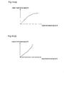
- the gamma correction circuit 1403 controls a gamma correction gain according to the value of the comparison signal E, performs gamma correction on an input luminance signal A, and outputs an output luminance signal B having a gamma correction characteristic as shown in figure 19(a) or 19(b). That is, when the maximum luminance level C is larger than the reference luminance level D, gamma correction for suppressing the white-side gradation is carried out as shown in figure 19(a), and when the maximum luminance level C is smaller than the reference luminance level D, inverse gamma correction for expanding the white-side gradation is carried out as shown in figure 19(b), whereby an output luminance signal B is obtained to be outputted to the matrix circuit 1404.
- the matrix circuit 1404 performs a matrix operation on the output luminance signal B and a chrominance signal Cin to obtain output signals R (red), G (green), and B (blue), and outputs these signals to the CRT 1405.
- the CRT 1405 is driven by the output signals R, G, and B, thereby obtaining a gradation-corrected image.
- comparison between the maximum luminance level C outputted from the maximum luminance level detection circuit 1404 and the reference luminance level D is performed by the comparison circuit 1402, and the gamma correction gain is controlled according to the comparison signal E, whereby gradation correction is carried out by analog feedback control such that the output luminance signal B becomes equal to the reference luminance signal D.
- analog feedback control such that the output luminance signal B becomes equal to the reference luminance signal D.
- the present invention is made in view of the existing situation described above and has for its object to provide a gradation correction device that can perform gradation correction using feedback processing even in digital fashion, and that can perform control with high accuracy.
- a gradation correction device corrects an input luminance signal of an image according to an output luminance signal so that an output having a predetermined characteristic in relation to the input luminance signal can be obtained, which device comprises: a maximum output luminance level detection means for detecting a maximum output luminance level of the output luminance signal which has already been gradation-corrected; a first subtraction means for calculating a difference value between the maximum output luminance level which is outputted from the maximum output luminance level detection means, and a first reference luminance level which is supplied from the outside; a correction gain adjustable amount generation means for outputting a predetermined adjustable amount according to the difference value, on the basis of a characteristic curve such that a change in the adjustable amount to be outputted is increased as the absolute value of the difference value outputted from the first subtraction means becomes larger; a correction gain generation means for adding or subtracting the adjustable amount outputted from the correction gain adjustable amount generation means to/from the current correction gain, and outputting the result as a correction gain; a
- a blooming luminance level that is a luminance level at which an image displayed on an image receiving tube blooms is employed as the first reference luminance level and the second reference luminance level.
- the gradation correction device as defined in Claim 1 further comprises: a maximum input luminance level detection means for detecting a maximum luminance level of the input luminance signal; a comparison means for comparing the maximum input luminance level outputted from the maximum input luminance level detection means, with the first reference luminance level; an addition means for adding the gamma correction amount outputted from the multiplication means to the input luminance signal, thereby performing gamma correction on the input luminance signal; and an output selection means for selecting either the output of the second subtraction means or the output of the addition means according to the result of the comparison by the comparison means, and outputting the selected one; wherein, when the maximum input luminance level is larger than the first reference luminance level in the comparison means, the output of the second subtraction means is selected by the selection means and outputted to perform gamma correction; on the other hand, when the maximum input luminance level is smaller than the first reference luminance level, the output of the addition means is selected by the selection means and outputted to perform gamma correction; on the other hand
- a gradation correction device corrects an input luminance signal of an image according to an output luminance signal so that an output having a predetermined characteristic in relation to the input luminance signal can be obtained, which device comprises: a minimum output luminance level detection means for detecting a minimum output luminance level of the output luminance signal which has already been gradation-corrected; a first subtraction means for calculating a difference value between the minimum output luminance level which is outputted from the minimum output luminance level detection means, and a first reference luminance level which is supplied from the outside; a correction gain adjustable amount generation means for outputting a predetermined adjustable amount according to the difference value, on the basis of a characteristic curve such that a change in the adjustable amount to be outputted is increased as the absolute value of the difference value outputted from the first subtraction means becomes larger; a correction gain generation means for adding or subtracting the adjustable amount outputted from the correction gain adjustable amount generation means to/from the current correction gain, and outputting the result as a correction gain; a black
- the gradation correction device as defined in Claim 1 further comprises: a minimum output luminance level detection means for detecting a minimum output luminance level of the output luminance signal which has already been gradation-corrected; a third subtraction means for calculating a difference value between the minimum output luminance level which is outputted from the minimum output luminance level detection means, and a third reference luminance level which is supplied from the outside; a black level correction signal generation means for generating a black level correction signal for the input luminance signal outputted from the second subtraction means, on the basis of a fourth reference luminance level which is supplied from the outside; a second multiplication means for multiplying a second correction gain which is obtained by the correction gain adjustable amount generation means and the correction gain generation means, by the output of the black level correction signal generation means, on the basis of the absolute value of the difference value which is outputted from the third subtraction means; and a fourth subtraction means for subtracting the output of the second multiplication means from the output of the second subtraction means,
- the gradation correction device as defined in Claim 4 further comprises: a maximum output luminance level detection means for detecting a maximum output luminance level of the output luminance signal which has already been gradation-corrected; a third subtraction means for calculating a difference value between the maximum output luminance level which is outputted from the maximum output luminance level detection means, and a third reference luminance level which is supplied from the outside; a gamma correction signal generation means for generating a gamma correction signal for the luminance signal which is outputted from the second subtraction means, on the basis of a fourth reference luminance level which is supplied from the outside; a second multiplication means for multiplying a second correction gain which is obtained by the correction gain adjustable amount generation means and the correction gain generation means, by the output of the gamma correction signal generation means, on the basis of the absolute value of the difference value which is outputted from the third subtraction means; and a fourth subtraction means for subtracting the output of the second multiplication means from the output
- a gradation correction device for correcting an input luminance signal of an image according to an output luminance signal so that an output having a predetermined characteristic in relation to the input luminance signal can be obtained, which device comprises: a maximum output luminance level detection means for detecting a maximum output luminance level of the output luminance signal which has already been gradation-corrected; a first subtraction means for calculating a difference value between the maximum output luminance level which is outputted from the maximum output luminance level detection means, and a first reference luminance level which is supplied from the outside; a correction gain adjustable amount generation means for outputting a predetermined adjustable amount according to the difference value, on the basis of a characteristic curve such that a change in the adjustable amount to be outputted is increased as the absolute value of the difference value outputted from the first subtraction means becomes larger; a correction gain generation means for adding or subtracting the adjustable amount outputted from the correction gain adjustable amount generation means to/from the current correction gain, and outputting the
- the luminance signal can be converged into a predetermined luminance level with high responsivity even in digital feedback control, and gamma correction, which is one of gradation corrections that have conventionally been performed in analog feedback control, can be realized by digital feedback control.
- a blooming luminance level that is a luminance level at which an image displayed on an image receiving tube blooms is employed as the first reference luminance level and the second reference luminance level. Therefore, the maximum output luminance level of the output luminance signal is prevented from becoming larger than the blooming luminance level, thereby performing gradation correction which is effective at reducing blooming that is a phenomenon unique to a CRT.
- the gradation correction device further comprises: a maximum input luminance level detection means for detecting a maximum luminance level of the input luminance signal; a comparison means for comparing the maximum input luminance level outputted from the maximum input luminance level detection means, with the first reference luminance level; an addition means for adding the gamma correction amount outputted from the multiplication means to the input luminance signal, thereby performing gamma correction on the input luminance signal; and an output selection means for selecting either the output of the second subtraction means or the output of the addition means according to the result of the comparison by the comparison means, and outputting the selected one; wherein, when the maximum input luminance level is larger than the first reference luminance level in the comparison means, the output of the second subtraction means is selected by the selection means and outputted to perform gamma correction; on the other hand, when the maximum input luminance level is smaller than the first reference luminance level, the output of the addition means is selected by the selection means and outputted to perform inverse
- a gradation correction device for correcting an input luminance signal of an image according to an output luminance signal so that an output having a predetermined characteristic in relation to the input luminance signal can be obtained, which device comprises: a minimum output luminance level detection means for detecting a minimum output luminance level of the output luminance signal which has already been gradation-corrected; a first subtraction means for calculating a difference value between the minimum output luminance level which is outputted from the minimum output luminance level detection means, and a first reference luminance level which is supplied from the outside; a correction gain adjustable amount generation means for outputting a predetermined adjustable amount according to the difference value, on the basis of a characteristic curve such that a change in the adjustable amount to be outputted is increased as the absolute value of the difference value outputted from the first subtraction means becomes larger; a correction gain generation means for adding or subtracting the adjustable amount outputted from the correction gain adjustable amount generation means to/from the current correction gain, and outputting the result as a
- the luminance signal can be converged into a predetermined luminance level with high responsivity even in digital feedback control, and black level correction, which is one of gradation corrections that have conventionally been performed in analog feedback control, can be realized by digital feedback control.
- the gradation correction device further comprises: a minimum output luminance level detection means for detecting a minimum output luminance level of the output luminance signal which has already been gradation-corrected; a third subtraction means for calculating a difference value between the minimum output luminance level which is outputted from the minimum output luminance level detection means, and a third reference luminance level which is supplied from the outside; a black level correction signal generation means for generating a black level correction signal for the input luminance signal outputted from the second subtraction means, on the basis of a fourth reference luminance level which is supplied from the outside; a second multiplication means for multiplying a second correction gain which is obtained by the correction gain adjustable amount generation means and the correction gain generation means, by the output of the black level correction signal generation means, on the basis of the absolute value of the difference value which is outputted from the third subtraction means; and a fourth subtraction means for subtracting the output of the second multiplication means from the output of the second subtraction means,
- the gradation correction device further comprises: a maximum output luminance level detection means for detecting a maximum output luminance level of the output luminance signal which has already been gradation-corrected; a third subtraction means for calculating a difference value between the maximum output luminance level which is outputted from the maximum output luminance level detection means, and a third reference luminance level which is supplied from the outside; a gamma correction signal generation means for generating a gamma correction signal for the luminance signal which is outputted from the second subtraction means, on the basis of a fourth reference luminance level which is supplied from the outside; a second multiplication means for multiplying a second correction gain which is obtained by the correction gain adjustable amount generation means and the correction gain generation means, by the output of the gamma correction signal generation means, on the basis of the absolute value of the difference value which is outputted from the third subtraction means; and a fourth subtraction means for subtracting the output of the second multiplication means from the output of
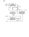
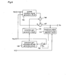
- FIG. 1 is a block diagram illustrating the construction of a gradation correction device according to the first embodiment.
- the gradation correction device is provided with a maximum output luminance level detection circuit 101 for detecting a maximum luminance level of an output luminance signal Yo; a first subtraction circuit 102 for subtracting a first reference luminance level Yb1 from the output of the maximum output luminance level detection circuit 101; a correction gain adjustable amount generation circuit 103 for calculating a correction gain adjustable amount on the basis of the output of the first subtraction circuit 102; a correction gain generation circuit 104 for generating a correction gain that is a function according to the calculation result of the correction gain adjustable amount generation circuit 103; a gamma correction signal generation circuit 105 for receiving an input luminance signal Yin and a second reference luminance signal Yb2, and generating a gamma correction signal; a multiplication circuit 106 for multiplying the output Gs of the gamma correction signal generation circuit 105 by the output Hg of the correction gain generation circuit
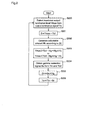
- step S200 the maximum output luminance level detection circuit 101 detects a maximum output luminance level Ymax within one field of the output luminance signal Yo, and outputs it to the first subtraction circuit 102.
- a maximum luminance level within several fields of the output luminance signal Yo may be obtained as a maximum output luminance level Ymax.
- step S202 the correction gain adjustable amount generation circuit 103 performs control such that an adjustable amount Hk of a correction gain Hg is increased as an absolute value
- the sign (positive or negative) of the difference value S is also transmitted to the correction gain generation circuit 104.
- the operation of the correction gain adjustable amount generation circuit 103 will be described with reference to the drawing.
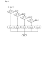
- Figure 3 is a flowchart for explaining a method of generating an adjustable amount Hk in the correction gain adjustable amount generation circuit.
- K1, K2, K3, and K4 (K1 ⁇ K2 ⁇ K3 ⁇ K4) are arbitrarily settable comparison levels to be used for determining the size of the absolute value
- J1, J2, J3, and J4 (J1 ⁇ J2 ⁇ J3 ⁇ J4) are adjustable amounts Hk that are adaptive to the size of the absolute value
- the values of J1 ⁇ J4 can be arbitrarily set.
- the adjustable amount Hk takes any of the values J1 ⁇ J4 according to the size of the absolute value
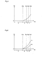
- Figure 4 shows an example of the relationship between the adjustable amount Hk and the absolute value
- the correction gain adjustable amount generation circuit 103 functions so as to increase the adjustable amount Hk as the absolute value
- the correction gain generation circuit 104 obtains a new correction gain Hg by adding or subtracting the adjustable amount Hk to/from the current correction gain Hg, according to the result of comparison between the maximum output luminance level Ymax and the first reference luminance level Yb1, and outputs the new correction gain Hg to the multiplication circuit 106.
- step S204 the gamma correction signal generation circuit 105 obtains a gamma correction signal Gs corresponding to the input luminance signal Yin, on the basis of the second reference luminance level Yb2 that is supplied from the outside, and outputs the gamma correction signal Gs to the multiplication circuit 106.
- Figure 5 shows the relationship between the input luminance signal Yin and the gamma correction signal Gs which is generated by the gamma correction signal generation circuit 105.
- the x-axis indicates the value of the input luminance signal Yin
- the y-axis indicates the value of the gamma correction signal Gs.
- slice levels SLa, SLb, and SLc (SLa ⁇ SLb ⁇ SLc), which are determined on the basis of the second reference luminance level Yb2, are set.
- the gamma correction signal generation circuit 105 Based on these slice levels SLa, SLb, and SLc, the gamma correction signal generation circuit 105 outputs the gamma correction signal Gs for the input luminance signal Yin, as a polygonal-line characteristic shown in figure 5.
- the gamma correction signal Gs is obtained by formula (4) when the level of the input luminance signal Yin is in an area A shown in figure 6, by formula (5) when the level of the Yin is in an area B, by formula (6) when the level of the Yin is in an area C, and by formula (7) when the level of the Yin is in an area D.
- the difference values between the input luminance signal Yin and the slice levels SLa, SLb, and SLc are obtained, and the respective difference values are added, whereby the gamma correction signal Gs for the input luminance signal Yin can be obtained as the polygonal-line characteristic shown in figure 5.
- the three slice levels are obtained on the basis of the second reference luminance level Yb2, these slice levels may be supplied from the outside.
- the gamma correction signal Gs is obtained using the three points of slice levels, it may be obtained using more or less than three points of slice levels.
- step S205 the multiplication circuit 106 multiplies the gamma correction signal Gs by the correction gain Hg to obtain a gamma correction amount Gr, and outputs it to the second subtraction circuit 107.
- Figure 6 is a diagram illustrating the relationship between the gamma correction amount Gr and the input luminance signal Yin.
- a polygonal-line characteristic T1 is obtained when the correction gain Hg is relatively large, and a polygonal-line characteristic T2 is obtained when the correction gain Hg is relatively small.
- step S206 the second subtraction circuit 107 subtracts the gamma correction amount Gr from the input luminance signal Yin to obtain the result as an output luminance signal Yo.
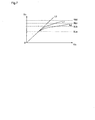
- Figure 7 is a diagram illustrating the relationship between the input luminance signal Yin and the output luminance signal Yo.
- an I/O characteristic L0 is obtained when the input luminance signal Yin is not subjected to gamma correction
- an I/O characteristic L1 is obtained when the signal Yin is subjected to gamma correction weakly
- an I/O characteristic L2 is obtained when the signal Yin is subjected to gamma correction strongly.
- the white-side gradation of the output luminance signal Yo outputted from the second subtraction circuit 107 is suppressed by the gamma correction.
- the output luminance level Yo is outputted from the second subtraction circuit 107 by digital feedback control such that the maximum output luminance level Ymax becomes equal to the first reference luminance level Yb1.
- the output luminance signal Yo so obtained is again captured by the maximum output luminance level detection circuit 101 in step S200, and thus feedback control is carried out.
- the process shown in figure 2 is desired to be completed, timing-wise, within one vertical sync period to realize highly-accurate feedback.
- correction gain adjustable amount generation circuit 103 and the correction gain generation circuit 104 are described as separated block circuits, these circuits may be implemented by using a common arithmetic processing circuit such as a CPU.
- the gradation correction device is provided with the correction gain adjustable amount generation circuit 103 and the correction gain generation circuit 104, and the correction gain adjustable amount generation circuit 103 generates a correction gain adjustable amount that makes a non-linear, accelerating, and monotonous increase with respect to the difference S between the reference luminance level Yb1 and the maximum luminance level as shown in figure 4, and greater gamma correction is carried out as the value of the difference is larger.
- digital feedback control in which the maximum output luminance level Ymax and the first reference luminance level Yb1 can be made equal to each other with high responsivity, is realized, and gamma correction, which is one of gradation corrections that have conventionally been performed in analog feedback control, can be realized by digital feedback control.
- FIG 8 is a block diagram illustrating a gradation correction device according to a modification of the first embodiment.
- the gradation correction device shown in figure 8 is different from the gradation correction device shown in figure 1 in that a blooming luminance level Ybu1 that is a luminance level at which blooming of an image occurs is employed instead of the first reference luminance level Yb1 and the second reference luminance level Yb2.
- the operating principles of the respective constituents are identical to those described for the gradation correction device shown in figure 1 and, therefore, repeated description is not necessary.
- the so-constructed gradation correction device shown in figure 8 employs the blooming luminance level Ybu1
- the maximum output luminance level Ymax of the output luminance signal Yo is prevented from being higher than the blooming luminance level Ybu1, whereby effective gradation correction which reduces "blooming" as a phenomenon unique to the CRT can be carried out.
- the gradation correction device may be constructed such that the first reference luminance level Yb1 and the second reference luminance level Yb2 are arbitrarily set from the outside.
- the first reference luminance level Yb1 and the second reference luminance level Yb2 can be adjusted while monitoring the actual image in the manufacture stage, whereby the effect of improper gamma correction can be controlled, resulting in an image faithful to the transmitted image.
- both of the first reference luminance level Yb1 and the second reference luminance level Yb2 are replaced with the blooming luminance level Ybu1
- only the first reference luminance level Yb1 may be replaced with the blooming luminance level Ybu1
- only the second reference luminance level Yb2 may be replaced with the blooming luminance level Ybu1.
- the correction characteristic can be changed according to the user operation, and gamma correction suited to the preference of the user can be carried out.
- the other luminance level that is not set at the blooming luminance level must be set at a level lower than the blooming level to prevent the gamma correction processing from failing.
- FIG. 9 is a block diagram illustrating the construction of a gradation correction device according to a second embodiment of the present invention.
- the gradation correction device shown in figure 9 is provided with, in addition to the constituents of the gradation correction device shown in figure 1, a maximum input luminance level detection circuit 801 for detecting a maximum input luminance level from the input luminance signal Yin; a comparison circuit 802 for comparing the output of the maximum input luminance level detection circuit 801 and the first reference luminance level Yb1; an addition circuit 803 for adding the input luminance signal Yin and the output of the multiplication circuit 106; and a selection circuit 804 for selecting either the output of the subtracter 107 or the output of the adder 803.
- a maximum input luminance level detection circuit 801 for detecting a maximum input luminance level from the input luminance signal Yin
- a comparison circuit 802 for comparing the output of the maximum input luminance level detection circuit 801 and the first reference luminance level Yb1
- the maximum input luminance level detection circuit 801 detects a maximum input luminance level Ymax2 within one field of the input luminance signal Yin, and outputs it to the comparison circuit 802. As for the maximum input luminance level Ymax2, a maximum luminance level within several fields of the input luminance signal Yin may be obtained.
- the comparison circuit 802 compares the maximum input luminance level Ymax2 with the first reference luminance level Yb1, and outputs the result of the comparison to the selection circuit 804.
- the addition circuit 803 adds the gamma correction amount Gr outputted from the multiplication circuit 106, to the input luminance signal Yin, and outputs the sum to the selection circuit 804.
- the selection circuit 804 selects the output of the second subtraction circuit 107 when the maximum input luminance level Ymax2 is higher than the first reference luminance level Yb1, or selects the output of the addition circuit 803 when the maximum input luminance level Ymax2 is lower than the first reference luminance level Yb1, and outputs the selected signal as an output luminance signal Yo.
- Figure 10(a) is a diagram illustrating the relationship between the input luminance signal Yin and the output luminance signal Yo when the maximum input luminance level Ymax2 is higher than the first reference luminance level Yb1 (Ymax2>Yb1).
- the selection circuit 804 selects the output of the second subtraction circuit 107, which output is obtained by subtracting the gamma correction amount Gr from the input luminance signal Yin, and therefore, gamma correction functions so as to suppress the white-side gradation of the luminance signal as shown in figure 10(a).
- figure 10(b) is a diagram illustrating the relationship between the input luminance signal Yin and the output luminance signal Yo when the maximum input luminance level Ymax2 is lower than the first reference luminance level Yb1 (Ymax2 ⁇ Yb1).
- the selection circuit 804 selects the output of the addition circuit 803, which output is obtained by adding the gamma correction amount Gr to the input luminance signal Yin, and therefore, gamma correction functions as inverse gamma correction for expanding the white-side gradation of the luminance signal as shown in figure 10(b).
- the gradation correction device is provided with the maximum input luminance level detection circuit 801 and the comparison circuit 802 for comparing the maximum input luminance level with the first reference luminance level, whereby gamma correction for suppressing the white-side gradation of the luminance signal can be carried out according to the result of the comparison between the input luminance signal and the first reference luminance level. Further, when the maximum input luminance level is lower than the reference value, it is judged that the white-side luminance level has a margin, and inverse gamma correction for expanding the white-side gradation is also carried out. Therefore, the white-side dynamic range of the image signal can be increased, resulting in a clearer and more dynamic image.
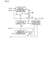
- FIG 11 is a block diagram illustrating the construction of a gradation correction device according to a third embodiment of the present invention.
- the gradation correction device shown in figure 11 is provided with a minimum output luminance level detection circuit 1001 instead of the maximum output luminance level detection circuit 101 in the gradation correction device shown in figure 1, and further, it is provided with a black level correction signal generation circuit 1002 instead of the gamma correction signal generation circuit 105 shown in figure 1.
- the black level correction signal generation circuit 1002 receives a third reference luminance level Yb3 which is supplied as an input from the outside, and the first subtraction circuit 102 receives a fourth reference luminance level Yb4 which is supplied as an input from the outside.
- the third and fourth reference luminance levels have the relationship of Yb3>Yb4.
- the minimum output luminance level detection circuit 1001 detects a minimum output luminance level Ymin within one field of the output luminance signal Yo, and outputs it to the first subtraction circuit 102. As for the minimum output luminance level Ymin, a minimum luminance level within several fields of the output luminance signal Yo may be obtained.
- the correction gain adjustable amount generation circuit 103 performs control such that the adjustable amount Hk of the correction gain Hg is increased as the absolute value
- the black level correction signal generation circuit 1002 obtains a black level correction signal Bs corresponding to the input luminance signal Yin on the basis of the third reference luminance level Yb3, and outputs it to the multiplication circuit 106.
- Figure 12 is a diagram illustrating the relationship between the input luminance signal Yin and the black level correction signal Bs obtained by the black level correction signal generation circuit 1002.
- the x-axis indicates the input luminance signal Yin while the y-axis indicates the value of the black level correction signal Bs.
- the third reference luminance level Yb3 is set.
- Bs b(Yin)
- the multiplication circuit 106 multiplies the black level correction signal Bs by the correction gain Hg to obtain a black level correction amount Br, and outputs it to the second subtraction circuit 107.
- Figure 13 is a diagram illustrating the relationship between the black level correction amount Br and the input luminance signal Yin.
- a straight-line characteristic T3 is obtained when the correction gain Hg is relatively large
- a straight-line characteristic T4 is obtained when the correction gain Hg is relatively small.
- FIG 14 is a diagram illustrating the relationship between the input luminance signal Yin and the output luminance signal Yo.
- an I/O characteristic L3 is obtained when the input luminance signal Yin is not subjected to correction
- an I/O characteristic L4 is obtained when the input signal Yin is subjected to black level correction weakly
- an I/O characteristic L5 is obtained when the input signal Yin is subjected to black level correction strongly.
- the black-side gradation of the output luminance signal Yo outputted from the second subtraction circuit 107 is expanded by the black level correction.
- the output luminance signal Yo is outputted from the second subtraction circuit 107 by digital feedback control such that the minimum output luminance level Ymin becomes equal to the fourth reference luminance level Yb4.
- correction gain adjustable amount generation circuit 103 and the correction gain generation circuit are shown as separated block circuits, these circuits may be implemented by using a common arithmetic processing circuit such as a CPU.
- the gradation correction device As described above, the gradation correction device according to the third embodiment is provided with the correction gain adjustable amount generation circuit 103 and the correction gain generation circuit 104 as in the first embodiment. Therefore, the gradation correction device can perform digital feedback control such that the maximum output luminance level Ymin becomes equal to the fourth reference luminance level Yb4 with high responsivity, whereby black level correction, which is one of gradation corrections that have conventionally been performed in analog feedback control, can be realized by digital feedback control.
- the third reference luminance level Yb3 and the fourth reference luminance level Yb4 according to the third embodiment may be arbitrarily set from the outside.
- the third reference luminance level Yb3 and the fourth reference luminance level Yb4 can be adjusted while monitoring the actual image in the manufacture stage, whereby the effect of improper black level correction is controlled, and a fine picture can be created.
- FIG. 15 is a block diagram illustrating the construction of a gradation correction device according to a fourth embodiment of the present invention.
- the gradation correction device shown in figure 15 is provided with both of the gamma correction mechanism of the gradation correction device shown in figure 1 and the black level correction mechanism shown in figure 11.
- the black-level-corrected luminance signal is subjected to gamma correction for suppressing the white-side gradation, thereby obtaining an output luminance signal Yo.
- reference character A denotes a common arithmetic processing unit including the first subtraction circuit 102, the correction gain adjustable amount generation circuit 103, and the correction gain generation circuit 104 which are shown in figures 1 and 11.
- a correction gain Hbg for black level correction and a correction gain Hgg for gamma correction are obtained by time-division processing.
- Figure 16 shows an example of a method for obtaining the correction gains Hbg and Hgg by time-division processing. That is, the common arithmetic processing unit A repeats a series of arithmetic processing for obtaining new correction gains Hbg and Hgg at the timing of a vertical sync signal V.
- the vertical sync signal V is used as a timing pulse for performing time-division processing
- other timing pulses such as a horizontal sync signal may be used.
- Figure 17 is a diagram illustrating the relationship between the input luminance signal Yin and the output luminance signal Yo.
- an I/O characteristic LA is obtained when no correction is carried out
- an I/O characteristic LB is obtained when both of black level correction and gamma level correction are carried out.
- the input luminance signal Yin is small, i.e., when the luminance level is low
- black level correction is carried out to obtain the output luminance signal Yo in which the black-side gradation is expanded.
- the input luminance signal Yin is large, i.e., when the luminance level is high, gamma correction is carried out to suppress the white-side gradation.
- both of black-side and white-side gradation corrections can be performed on the input luminance signal Yin, resulting in an image which is clearer and more dynamic than that obtained by the second or third embodiment.
- gamma correction is carried out after performing black level correction, gamma correction may be performed first and then the gamma-corrected-signal may be subjected to black level correction. Also in this case, the same effects as mentioned above are achieved.
- a gradation correction device for performing gradation correction on a luminance signal of an image
- digital feedback correction is performed with high accuracy, whereby, for example, gamma correction, which is one of gradation corrections in a video signal processing in digital fashion, can be realized.
Landscapes
- Engineering & Computer Science (AREA)
- Multimedia (AREA)
- Signal Processing (AREA)
- Physics & Mathematics (AREA)
- General Physics & Mathematics (AREA)
- Theoretical Computer Science (AREA)
- Picture Signal Circuits (AREA)
- Facsimile Image Signal Circuits (AREA)
- Image Processing (AREA)
- Television Receiver Circuits (AREA)
- Controls And Circuits For Display Device (AREA)
- Processing Of Color Television Signals (AREA)
Abstract
An object of the present invention is to provide a gradation correction device which can perform gradation correction using digital feedback processing, and furthermore, can control the digital feedback processing with high accuracy. <??>The gradation correction device is provided with a correction gain adjustable amount generation circuit (103) and a correction gain generation circuit (104), and the correction gain adjustable amount generation circuit (103) obtains a correction gain adjustable amount which is non-linear in relation to a difference S between a reference luminance level Yb1 and a maximum luminance level, and greater gamma correction is carried out as the value of the difference is larger. <IMAGE>
Description
The present invention relates to a gradation correction
device for performing gradation correction on a luminance signal
of an image in equipment for displaying an image and, more
particularly, to a gradation correction device having a
construction for digitally performing feedback correction that
has conventionally been carried out in analog fashion.
In recent years, as color television receivers have been
increased in size, many color television receivers are provided
with gradation correction devices such as a black level
correction circuit for expanding the gradation of a luminance
signal of an image toward the black side or a gamma correction
circuit, in order to display the image more clearly and
dynamically. Further, in order to improve the accuracy of
gradation correction, digital signal processing techniques have
increasingly been employed.
Figure 18 is a block diagram illustrating a conventional
gradation correction device for a luminance signal, which is
disclosed in Japanese Published Patent Application No. Hei.4-37263.
The gradation correction device shown in figure 18 is
provided with a maximum luminance level detection circuit 1401; a
comparison circuit 1402 for comparing the output of the maximum
luminance level detection circuit 1401 with a reference value; a
gamma correction circuit 1403 for performing gamma correction on
the basis of the output of the comparison circuit 1402; a matrix
circuit 1404 for supplying R, G, and B signals to a cathode ray
tube (CRT); and the CRT 1405.
Hereinafter, the operation will be described. The maximum
luminance level detection circuit 1401 receives an output
luminance signal B, detects a maximum luminance level C within
one field of the output luminance signal B, and outputs it to the
comparison circuit 1402.
The comparison circuit 1402 compares the maximum luminance
level C with a reference luminance level D which is supplied from
the outside, and outputs a comparison signal E to the gamma
correction circuit 1403.
The gamma correction circuit 1403 controls a gamma
correction gain according to the value of the comparison signal E,
performs gamma correction on an input luminance signal A, and
outputs an output luminance signal B having a gamma correction
characteristic as shown in figure 19(a) or 19(b). That is, when
the maximum luminance level C is larger than the reference
luminance level D, gamma correction for suppressing the white-side
gradation is carried out as shown in figure 19(a), and when
the maximum luminance level C is smaller than the reference
luminance level D, inverse gamma correction for expanding the
white-side gradation is carried out as shown in figure 19(b),
whereby an output luminance signal B is obtained to be outputted
to the matrix circuit 1404.
The matrix circuit 1404 performs a matrix operation on the
output luminance signal B and a chrominance signal Cin to obtain
output signals R (red), G (green), and B (blue), and outputs
these signals to the CRT 1405.
Then, the CRT 1405 is driven by the output signals R, G, and
B, thereby obtaining a gradation-corrected image.
In the conventional gradation correction device constituted
as described above, comparison between the maximum luminance
level C outputted from the maximum luminance level detection
circuit 1404 and the reference luminance level D is performed by
the comparison circuit 1402, and the gamma correction gain is
controlled according to the comparison signal E, whereby
gradation correction is carried out by analog feedback control
such that the output luminance signal B becomes equal to the
reference luminance signal D. However, as described above, in a
rising tide of digitization of video signal processing in recent
years, there is a necessity of shifting the feedback control
which has been carried out in analog fashion by the conventional
gradation correction device, to feedback control in digital
fashion.
The present invention is made in view of the existing
situation described above and has for its object to provide a
gradation correction device that can perform gradation correction
using feedback processing even in digital fashion, and that can
perform control with high accuracy.
A gradation correction device according to Claim 1 of the
present invention corrects an input luminance signal of an image
according to an output luminance signal so that an output having
a predetermined characteristic in relation to the input luminance
signal can be obtained, which device comprises: a maximum output
luminance level detection means for detecting a maximum output
luminance level of the output luminance signal which has already
been gradation-corrected; a first subtraction means for
calculating a difference value between the maximum output
luminance level which is outputted from the maximum output
luminance level detection means, and a first reference luminance
level which is supplied from the outside; a correction gain
adjustable amount generation means for outputting a predetermined
adjustable amount according to the difference value, on the basis
of a characteristic curve such that a change in the adjustable
amount to be outputted is increased as the absolute value of the
difference value outputted from the first subtraction means
becomes larger; a correction gain generation means for adding or
subtracting the adjustable amount outputted from the correction
gain adjustable amount generation means to/from the current
correction gain, and outputting the result as a correction gain;
a gamma correction signal generation means for generating a gamma
correction signal for the input luminance signal, on the basis of
a second reference luminance level which is supplied from the
outside; a multiplication means for multiplying the gamma
correction signal outputted from the gamma correction signal
generation means by the correction gain outputted from the
correction gain generation means, and outputting the result as a
gamma correction amount; and a second subtraction means for
subtracting the gamma correction amount outputted from the
multiplication means, from the input luminance signal, thereby
performing gamma correction on the input luminance signal.
According to Claim 2 of the present invention, in the
gradation correction device as defined in Claim 1, a blooming
luminance level that is a luminance level at which an image
displayed on an image receiving tube blooms is employed as the
first reference luminance level and the second reference
luminance level.
According to Claim 3 of the present invention, the gradation
correction device as defined in Claim 1 further comprises: a
maximum input luminance level detection means for detecting a
maximum luminance level of the input luminance signal; a
comparison means for comparing the maximum input luminance level
outputted from the maximum input luminance level detection means,
with the first reference luminance level; an addition means for
adding the gamma correction amount outputted from the
multiplication means to the input luminance signal, thereby
performing gamma correction on the input luminance signal; and an
output selection means for selecting either the output of the
second subtraction means or the output of the addition means
according to the result of the comparison by the comparison means,
and outputting the selected one; wherein, when the maximum input
luminance level is larger than the first reference luminance
level in the comparison means, the output of the second
subtraction means is selected by the selection means and
outputted to perform gamma correction; on the other hand, when
the maximum input luminance level is smaller than the first
reference luminance level, the output of the addition means is
selected by the selection means and outputted to perform inverse
gamma correction for expanding the white-side gradation of the
luminance signal.
A gradation correction device according to Claim 4 of the
present invention corrects an input luminance signal of an image
according to an output luminance signal so that an output having
a predetermined characteristic in relation to the input luminance
signal can be obtained, which device comprises: a minimum output
luminance level detection means for detecting a minimum output
luminance level of the output luminance signal which has already
been gradation-corrected; a first subtraction means for
calculating a difference value between the minimum output
luminance level which is outputted from the minimum output
luminance level detection means, and a first reference luminance
level which is supplied from the outside; a correction gain
adjustable amount generation means for outputting a predetermined
adjustable amount according to the difference value, on the basis
of a characteristic curve such that a change in the adjustable
amount to be outputted is increased as the absolute value of the
difference value outputted from the first subtraction means
becomes larger; a correction gain generation means for adding or
subtracting the adjustable amount outputted from the correction
gain adjustable amount generation means to/from the current
correction gain, and outputting the result as a correction gain;
a black level correction signal generation means for generating a
black level correction signal for the input luminance signal, on
the basis of a second reference luminance level which is supplied
from the outside; a multiplication means for multiplying the
black level correction signal outputted from the black level
correction signal generation means, by the correction gain
outputted from the correction gain generation means, and
outputting the result as a black level correction amount; and a
second subtraction means for subtracting the black level
correction amount outputted from the multiplication means, from
the input luminance signal, thereby performing black level
correction on the input luminance signal.
According to Claim 5 of the present invention, the gradation
correction device as defined in Claim 1 further comprises: a
minimum output luminance level detection means for detecting a
minimum output luminance level of the output luminance signal
which has already been gradation-corrected; a third subtraction
means for calculating a difference value between the minimum
output luminance level which is outputted from the minimum output
luminance level detection means, and a third reference luminance
level which is supplied from the outside; a black level
correction signal generation means for generating a black level
correction signal for the input luminance signal outputted from
the second subtraction means, on the basis of a fourth reference
luminance level which is supplied from the outside; a second
multiplication means for multiplying a second correction gain
which is obtained by the correction gain adjustable amount
generation means and the correction gain generation means, by the
output of the black level correction signal generation means, on
the basis of the absolute value of the difference value which is
outputted from the third subtraction means; and a fourth
subtraction means for subtracting the output of the second
multiplication means from the output of the second subtraction
means, thereby performing black level correction on the luminance
signal which has already been gamma-corrected.
According to Claim 6 of the present invention, the gradation
correction device as defined in Claim 4 further comprises: a
maximum output luminance level detection means for detecting a
maximum output luminance level of the output luminance signal
which has already been gradation-corrected; a third subtraction
means for calculating a difference value between the maximum
output luminance level which is outputted from the maximum output
luminance level detection means, and a third reference luminance
level which is supplied from the outside; a gamma correction
signal generation means for generating a gamma correction signal
for the luminance signal which is outputted from the second
subtraction means, on the basis of a fourth reference luminance
level which is supplied from the outside; a second multiplication
means for multiplying a second correction gain which is obtained
by the correction gain adjustable amount generation means and the
correction gain generation means, by the output of the gamma
correction signal generation means, on the basis of the absolute
value of the difference value which is outputted from the third
subtraction means; and a fourth subtraction means for subtracting
the output of the second multiplication means from the output of
the second subtraction means, thereby performing gamma correction
on the luminance signal whose black level has already been
corrected.
As described above, according to Claim 1 of the present
invention, there is provided a gradation correction device for
correcting an input luminance signal of an image according to an
output luminance signal so that an output having a predetermined
characteristic in relation to the input luminance signal can be
obtained, which device comprises: a maximum output luminance
level detection means for detecting a maximum output luminance
level of the output luminance signal which has already been
gradation-corrected; a first subtraction means for calculating a
difference value between the maximum output luminance level which
is outputted from the maximum output luminance level detection
means, and a first reference luminance level which is supplied
from the outside; a correction gain adjustable amount generation
means for outputting a predetermined adjustable amount according
to the difference value, on the basis of a characteristic curve
such that a change in the adjustable amount to be outputted is
increased as the absolute value of the difference value outputted
from the first subtraction means becomes larger; a correction
gain generation means for adding or subtracting the adjustable
amount outputted from the correction gain adjustable amount
generation means to/from the current correction gain, and
outputting the result as a correction gain; a gamma correction
signal generation means for generating a gamma correction signal
for the input luminance signal, on the basis of a second
reference luminance level which is supplied from the outside; a
multiplication means for multiplying the gamma correction signal
outputted from the gamma correction signal generation means by
the correction gain outputted from the correction gain generation
means, and outputting the result as a gamma correction amount;
and a second subtraction means for subtracting the gamma
correction amount outputted from the multiplication means, from
the input luminance signal, thereby performing gamma correction
on the input luminance signal. Therefore, the luminance signal
can be converged into a predetermined luminance level with high
responsivity even in digital feedback control, and gamma
correction, which is one of gradation corrections that have
conventionally been performed in analog feedback control, can be
realized by digital feedback control.
According to Claim 2 of the present invention, in the
gradation correction device according to Claim 1, a blooming
luminance level that is a luminance level at which an image
displayed on an image receiving tube blooms is employed as the
first reference luminance level and the second reference
luminance level. Therefore, the maximum output luminance level
of the output luminance signal is prevented from becoming larger
than the blooming luminance level, thereby performing gradation
correction which is effective at reducing blooming that is a
phenomenon unique to a CRT.
According to Claim 3 of the present invention, the gradation
correction device according to Claim 1 further comprises: a
maximum input luminance level detection means for detecting a
maximum luminance level of the input luminance signal; a
comparison means for comparing the maximum input luminance level
outputted from the maximum input luminance level detection means,
with the first reference luminance level; an addition means for
adding the gamma correction amount outputted from the
multiplication means to the input luminance signal, thereby
performing gamma correction on the input luminance signal; and an
output selection means for selecting either the output of the
second subtraction means or the output of the addition means
according to the result of the comparison by the comparison means,
and outputting the selected one; wherein, when the maximum input
luminance level is larger than the first reference luminance
level in the comparison means, the output of the second
subtraction means is selected by the selection means and
outputted to perform gamma correction; on the other hand, when
the maximum input luminance level is smaller than the first
reference luminance level, the output of the addition means is
selected by the selection means and outputted to perform inverse
gamma correction for expanding the white-side gradation of the
luminance signal. Therefore, the white-side dynamic range of the
image signal can be enlarged, whereby a clearer and more dynamic
image can be obtained.
According to Claim 4 of the present invention, there is
provided a gradation correction device for correcting an input
luminance signal of an image according to an output luminance
signal so that an output having a predetermined characteristic in
relation to the input luminance signal can be obtained, which
device comprises: a minimum output luminance level detection
means for detecting a minimum output luminance level of the
output luminance signal which has already been gradation-corrected;
a first subtraction means for calculating a difference
value between the minimum output luminance level which is
outputted from the minimum output luminance level detection means,
and a first reference luminance level which is supplied from the
outside; a correction gain adjustable amount generation means for
outputting a predetermined adjustable amount according to the
difference value, on the basis of a characteristic curve such
that a change in the adjustable amount to be outputted is
increased as the absolute value of the difference value outputted
from the first subtraction means becomes larger; a correction
gain generation means for adding or subtracting the adjustable
amount outputted from the correction gain adjustable amount
generation means to/from the current correction gain, and
outputting the result as a correction gain; a black level
correction signal generation means for generating a black level
correction signal for the input luminance signal, on the basis of
a second reference luminance level which is supplied from the
outside; a multiplication means for multiplying the black level
correction signal outputted from the black level correction
signal generation means, by the correction gain outputted from
the correction gain generation means, and outputting the result
as a black level correction amount; and a second subtraction
means for subtracting the black level correction amount outputted
from the multiplication means, from the input luminance signal,
thereby performing black level correction on the input luminance
signal. Therefore, the luminance signal can be converged into a
predetermined luminance level with high responsivity even in
digital feedback control, and black level correction, which is
one of gradation corrections that have conventionally been
performed in analog feedback control, can be realized by digital
feedback control.
According to Claim 5 of the present invention, the gradation
correction device according to Claim 1 further comprises: a
minimum output luminance level detection means for detecting a
minimum output luminance level of the output luminance signal
which has already been gradation-corrected; a third subtraction
means for calculating a difference value between the minimum
output luminance level which is outputted from the minimum output
luminance level detection means, and a third reference luminance
level which is supplied from the outside; a black level
correction signal generation means for generating a black level
correction signal for the input luminance signal outputted from
the second subtraction means, on the basis of a fourth reference
luminance level which is supplied from the outside; a second
multiplication means for multiplying a second correction gain
which is obtained by the correction gain adjustable amount
generation means and the correction gain generation means, by the
output of the black level correction signal generation means, on
the basis of the absolute value of the difference value which is
outputted from the third subtraction means; and a fourth
subtraction means for subtracting the output of the second
multiplication means from the output of the second subtraction
means, thereby performing black level correction on the luminance
signal which has already been gamma-corrected. Therefore, both
of black-side and white-side gradations of the input luminance
signal can be corrected, whereby a clearer and more dynamic image
can be obtained.
According to Claim 6 of the present invention, the gradation
correction device according to Claim 4 further comprises: a
maximum output luminance level detection means for detecting a
maximum output luminance level of the output luminance signal
which has already been gradation-corrected; a third subtraction
means for calculating a difference value between the maximum
output luminance level which is outputted from the maximum output
luminance level detection means, and a third reference luminance
level which is supplied from the outside; a gamma correction
signal generation means for generating a gamma correction signal
for the luminance signal which is outputted from the second
subtraction means, on the basis of a fourth reference luminance
level which is supplied from the outside; a second multiplication
means for multiplying a second correction gain which is obtained
by the correction gain adjustable amount generation means and the
correction gain generation means, by the output of the gamma
correction signal generation means, on the basis of the absolute
value of the difference value which is outputted from the third
subtraction means; and a fourth subtraction means for subtracting
the output of the second multiplication means from the output of
the second subtraction means, thereby performing gamma correction
on the luminance signal whose black level has already been
corrected. Therefore, both of black-side and white-side
gradations of the input luminance signal can be corrected,
whereby a clearer and more dynamic image can be obtained.
Hereinafter, a gradation correction device according to a
first embodiment of the present invention will be described with
reference to the drawing.
Figure 1 is a block diagram illustrating the construction of
a gradation correction device according to the first embodiment.
With reference to figure 1, the gradation correction device is
provided with a maximum output luminance level detection circuit
101 for detecting a maximum luminance level of an output
luminance signal Yo; a first subtraction circuit 102 for
subtracting a first reference luminance level Yb1 from the output
of the maximum output luminance level detection circuit 101; a
correction gain adjustable amount generation circuit 103 for
calculating a correction gain adjustable amount on the basis of
the output of the first subtraction circuit 102; a correction
gain generation circuit 104 for generating a correction gain that
is a function according to the calculation result of the
correction gain adjustable amount generation circuit 103; a gamma
correction signal generation circuit 105 for receiving an input
luminance signal Yin and a second reference luminance signal Yb2,
and generating a gamma correction signal; a multiplication
circuit 106 for multiplying the output Gs of the gamma correction
signal generation circuit 105 by the output Hg of the correction
gain generation circuit 104; and a second subtraction circuit 107
for subtracting the output Gr of the multiplication circuit 106
from the input luminance signal Yin. In figure 1, V is a
vertical sync signal which is input to the maximum output
luminance level detection circuit 101.
Hereinafter, the operation of the gradation correction
device constructed as described above will be described with
reference to a flowchart shown in figure 2.
When processing is started, in step S200, the maximum output
luminance level detection circuit 101 detects a maximum output
luminance level Ymax within one field of the output luminance
signal Yo, and outputs it to the first subtraction circuit 102.
A maximum luminance level within several fields of the output
luminance signal Yo may be obtained as a maximum output luminance
level Ymax.
In step S201, the first subtraction circuit 102 calculates a
difference value S between the maximum output luminance level
Ymax and the first reference luminance level Yb1 that is supplied
from the outside, as follows,
S = Ymax - Yb1
and outputs it to the correction gain adjustable amount
generation circuit 103.
In step S202, the correction gain adjustable amount
generation circuit 103 performs control such that an adjustable
amount Hk of a correction gain Hg is increased as an absolute
value |S| of the difference value S becomes larger, and
conversely, the adjustable amount Hk of the correction gain Hg is
decreased as the absolute value |S| becomes smaller, and outputs
the adjustable amount Hk to the correction gain generation
circuit 104. At this time, the sign (positive or negative) of
the difference value S is also transmitted to the correction gain
generation circuit 104. Hereinafter, the operation of the
correction gain adjustable amount generation circuit 103 will be
described with reference to the drawing.
Figure 3 is a flowchart for explaining a method of
generating an adjustable amount Hk in the correction gain
adjustable amount generation circuit. In figure 3, K1, K2, K3,
and K4 (K1<K2<K3<K4) are arbitrarily settable comparison levels
to be used for determining the size of the absolute value |S|,
and J1, J2, J3, and J4 (J1<J2<J3<J4) are adjustable amounts Hk
that are adaptive to the size of the absolute value |S|. The
values of J1~J4 can be arbitrarily set. The adjustable amount
Hk takes any of the values J1~J4 according to the size of the
absolute value |S|, on the basis of the flow shown in figure 2.
Figure 4 shows an example of the relationship between the
adjustable amount Hk and the absolute value |S| in the correction
gain adjustable amount generation circuit 103.
As shown in figure 4, the correction gain adjustable amount
generation circuit 103 functions so as to increase the adjustable
amount Hk as the absolute value |S| is larger, and decrease the
adjustable amount Hk as the absolute value |S| is smaller.
In step S203, the correction gain generation circuit 104
obtains a new correction gain Hg by adding or subtracting the
adjustable amount Hk to/from the current correction gain Hg,
according to the result of comparison between the maximum output
luminance level Ymax and the first reference luminance level Yb1,
and outputs the new correction gain Hg to the multiplication
circuit 106. To be specific, when the maximum output luminance
level Ymax is larger than the first reference luminance level Yb1,
the correction gain generation circuit 104 obtains the correction
gain Hg as follows,
Hg = Hg + Hk
thereby to increase the correction gain. Conversely, when the
maximum output luminance level Ymax is smaller than the first
reference luminance level Yb1, the correction gain generation
circuit 104 obtains the correction gain Hg as follows,
Hg = Hg - Hk
thereby to decrease the correction gain.
When the Ymax is equal to the Yb1, since the feedback is
converged, the adjustable amount Hk becomes zero and the size of
the correction gain Hg becomes constant.
In step S204, the gamma correction signal generation circuit
105 obtains a gamma correction signal Gs corresponding to the
input luminance signal Yin, on the basis of the second reference
luminance level Yb2 that is supplied from the outside, and
outputs the gamma correction signal Gs to the multiplication
circuit 106.
Figure 5 shows the relationship between the input luminance
signal Yin and the gamma correction signal Gs which is generated
by the gamma correction signal generation circuit 105. In figure
5, the x-axis indicates the value of the input luminance signal
Yin, and the y-axis indicates the value of the gamma correction
signal Gs. On the x-axis, slice levels SLa, SLb, and SLc
(SLa<SLb<SLc), which are determined on the basis of the second
reference luminance level Yb2, are set. Based on these slice
levels SLa, SLb, and SLc, the gamma correction signal generation
circuit 105 outputs the gamma correction signal Gs for the input
luminance signal Yin, as a polygonal-line characteristic shown in
figure 5. The gamma correction signal Gs is obtained by Gs =
g(Yin), and the function g(Yin) is, for example, represented by,
g(Yin) = 0
where (Yin≦SLa)
g(Yin) = Yin-SLa
where (SLa<Yin≦SLb)
g(Yin) = (Yin-SLa)+(Yin-SLb)
where (SLb<Yin≦SLc)
g(Yin) = (Yin-SLa)+(Yin-SLb)+(Yin-SLc)
where (SLc<Y)
That is, the gamma correction signal Gs is obtained by
formula (4) when the level of the input luminance signal Yin is
in an area A shown in figure 6, by formula (5) when the level of
the Yin is in an area B, by formula (6) when the level of the Yin
is in an area C, and by formula (7) when the level of the Yin is
in an area D.
In this way, the difference values between the input
luminance signal Yin and the slice levels SLa, SLb, and SLc are
obtained, and the respective difference values are added, whereby
the gamma correction signal Gs for the input luminance signal Yin
can be obtained as the polygonal-line characteristic shown in
figure 5. While in this embodiment the three slice levels are
obtained on the basis of the second reference luminance level Yb2,
these slice levels may be supplied from the outside. Furthermore,
while the gamma correction signal Gs is obtained using the three
points of slice levels, it may be obtained using more or less
than three points of slice levels.
In step S205, the multiplication circuit 106 multiplies the
gamma correction signal Gs by the correction gain Hg to obtain a
gamma correction amount Gr, and outputs it to the second
subtraction circuit 107.
Figure 6 is a diagram illustrating the relationship between
the gamma correction amount Gr and the input luminance signal Yin.
In figure 6, a polygonal-line characteristic T1 is obtained when
the correction gain Hg is relatively large, and a polygonal-line
characteristic T2 is obtained when the correction gain Hg is
relatively small. As is evident from figure 6, the larger the
correction gain Hg is, the larger the value of the gamma
correction amount Gr becomes.
In step S206, the second subtraction circuit 107 subtracts
the gamma correction amount Gr from the input luminance signal
Yin to obtain the result as an output luminance signal Yo.
Figure 7 is a diagram illustrating the relationship between
the input luminance signal Yin and the output luminance signal Yo.
In figure 7, an I/O characteristic L0 is obtained when the input
luminance signal Yin is not subjected to gamma correction, an I/O
characteristic L1 is obtained when the signal Yin is subjected to
gamma correction weakly, and an I/O characteristic L2 is obtained
when the signal Yin is subjected to gamma correction strongly.
As is evident from figure 7, the white-side gradation of the
output luminance signal Yo outputted from the second subtraction
circuit 107 is suppressed by the gamma correction. Further, the
output luminance level Yo is outputted from the second
subtraction circuit 107 by digital feedback control such that the
maximum output luminance level Ymax becomes equal to the first
reference luminance level Yb1.
The output luminance signal Yo so obtained is again captured
by the maximum output luminance level detection circuit 101 in
step S200, and thus feedback control is carried out.
The process shown in figure 2 is desired to be completed,
timing-wise, within one vertical sync period to realize highly-accurate
feedback.
While in this embodiment the correction gain adjustable
amount generation circuit 103 and the correction gain generation
circuit 104 are described as separated block circuits, these
circuits may be implemented by using a common arithmetic
processing circuit such as a CPU.
According to the first embodiment, the gradation correction
device is provided with the correction gain adjustable amount
generation circuit 103 and the correction gain generation circuit
104, and the correction gain adjustable amount generation circuit
103 generates a correction gain adjustable amount that makes a
non-linear, accelerating, and monotonous increase with respect to
the difference S between the reference luminance level Yb1 and
the maximum luminance level as shown in figure 4, and greater
gamma correction is carried out as the value of the difference is
larger. Therefore, digital feedback control, in which the
maximum output luminance level Ymax and the first reference
luminance level Yb1 can be made equal to each other with high
responsivity, is realized, and gamma correction, which is one of
gradation corrections that have conventionally been performed in
analog feedback control, can be realized by digital feedback
control.
Figure 8 is a block diagram illustrating a gradation
correction device according to a modification of the first
embodiment. The gradation correction device shown in figure 8 is
different from the gradation correction device shown in figure 1
in that a blooming luminance level Ybu1 that is a luminance level
at which blooming of an image occurs is employed instead of the
first reference luminance level Yb1 and the second reference
luminance level Yb2. The operating principles of the respective
constituents are identical to those described for the gradation
correction device shown in figure 1 and, therefore, repeated
description is not necessary.
Since the so-constructed gradation correction device shown
in figure 8 employs the blooming luminance level Ybu1, the
maximum output luminance level Ymax of the output luminance
signal Yo is prevented from being higher than the blooming
luminance level Ybu1, whereby effective gradation correction
which reduces "blooming" as a phenomenon unique to the CRT can be
carried out.
The gradation correction device according to the first
embodiment may be constructed such that the first reference
luminance level Yb1 and the second reference luminance level Yb2
are arbitrarily set from the outside. In this construction, the
first reference luminance level Yb1 and the second reference
luminance level Yb2 can be adjusted while monitoring the actual
image in the manufacture stage, whereby the effect of improper
gamma correction can be controlled, resulting in an image
faithful to the transmitted image.
While in the modification of this embodiment both of the
first reference luminance level Yb1 and the second reference
luminance level Yb2 are replaced with the blooming luminance
level Ybu1, only the first reference luminance level Yb1 may be
replaced with the blooming luminance level Ybu1, or only the
second reference luminance level Yb2 may be replaced with the
blooming luminance level Ybu1. Thereby, the correction
characteristic can be changed according to the user operation,
and gamma correction suited to the preference of the user can be
carried out. When such construction is employed, the other
luminance level that is not set at the blooming luminance level
must be set at a level lower than the blooming level to prevent
the gamma correction processing from failing.
Figure 9 is a block diagram illustrating the construction of
a gradation correction device according to a second embodiment of
the present invention. The gradation correction device shown in
figure 9 is provided with, in addition to the constituents of the
gradation correction device shown in figure 1, a maximum input
luminance level detection circuit 801 for detecting a maximum
input luminance level from the input luminance signal Yin; a
comparison circuit 802 for comparing the output of the maximum
input luminance level detection circuit 801 and the first
reference luminance level Yb1; an addition circuit 803 for adding
the input luminance signal Yin and the output of the
multiplication circuit 106; and a selection circuit 804 for
selecting either the output of the subtracter 107 or the output
of the adder 803.
Hereinafter, the operation of the gradation correction
device so constructed will be described.
The maximum input luminance level detection circuit 801
detects a maximum input luminance level Ymax2 within one field of
the input luminance signal Yin, and outputs it to the comparison
circuit 802. As for the maximum input luminance level Ymax2, a
maximum luminance level within several fields of the input
luminance signal Yin may be obtained.
The comparison circuit 802 compares the maximum input
luminance level Ymax2 with the first reference luminance level
Yb1, and outputs the result of the comparison to the selection
circuit 804.
The addition circuit 803 adds the gamma correction amount Gr
outputted from the multiplication circuit 106, to the input
luminance signal Yin, and outputs the sum to the selection
circuit 804.
Based on the result of the comparison by the comparison
circuit 802, the selection circuit 804 selects the output of the
second subtraction circuit 107 when the maximum input luminance
level Ymax2 is higher than the first reference luminance level
Yb1, or selects the output of the addition circuit 803 when the
maximum input luminance level Ymax2 is lower than the first
reference luminance level Yb1, and outputs the selected signal as
an output luminance signal Yo.
The constituents other than described above are identical to
those shown in figure 1 and, therefore, repeated description is
not necessary.
Figure 10(a) is a diagram illustrating the relationship
between the input luminance signal Yin and the output luminance
signal Yo when the maximum input luminance level Ymax2 is higher
than the first reference luminance level Yb1 (Ymax2>Yb1). When
the maximum input luminance level Ymax2 is higher than the first
reference luminance level Yb1, the selection circuit 804 selects
the output of the second subtraction circuit 107, which output is
obtained by subtracting the gamma correction amount Gr from the
input luminance signal Yin, and therefore, gamma correction
functions so as to suppress the white-side gradation of the
luminance signal as shown in figure 10(a).
On the other hand, figure 10(b) is a diagram illustrating
the relationship between the input luminance signal Yin and the
output luminance signal Yo when the maximum input luminance level
Ymax2 is lower than the first reference luminance level Yb1
(Ymax2<Yb1). When the maximum input luminance level Ymax2 is
lower than the first reference luminance level Yb1, the selection
circuit 804 selects the output of the addition circuit 803, which
output is obtained by adding the gamma correction amount Gr to
the input luminance signal Yin, and therefore, gamma correction
functions as inverse gamma correction for expanding the white-side
gradation of the luminance signal as shown in figure 10(b).
As described above, the gradation correction device
according to the second embodiment is provided with the maximum
input luminance level detection circuit 801 and the comparison
circuit 802 for comparing the maximum input luminance level with
the first reference luminance level, whereby gamma correction for
suppressing the white-side gradation of the luminance signal can
be carried out according to the result of the comparison between
the input luminance signal and the first reference luminance
level. Further, when the maximum input luminance level is lower
than the reference value, it is judged that the white-side
luminance level has a margin, and inverse gamma correction for
expanding the white-side gradation is also carried out.
Therefore, the white-side dynamic range of the image signal can
be increased, resulting in a clearer and more dynamic image.
Figure 11 is a block diagram illustrating the construction
of a gradation correction device according to a third embodiment
of the present invention. The gradation correction device shown
in figure 11 is provided with a minimum output luminance level
detection circuit 1001 instead of the maximum output luminance
level detection circuit 101 in the gradation correction device
shown in figure 1, and further, it is provided with a black level
correction signal generation circuit 1002 instead of the gamma
correction signal generation circuit 105 shown in figure 1. The
black level correction signal generation circuit 1002 receives a
third reference luminance level Yb3 which is supplied as an input
from the outside, and the first subtraction circuit 102 receives
a fourth reference luminance level Yb4 which is supplied as an
input from the outside. Usually, the third and fourth reference
luminance levels have the relationship of Yb3>Yb4.
Hereinafter, the operation of the gradation correction
device so constructed will be described.
The minimum output luminance level detection circuit 1001
detects a minimum output luminance level Ymin within one field of
the output luminance signal Yo, and outputs it to the first
subtraction circuit 102. As for the minimum output luminance
level Ymin, a minimum luminance level within several fields of
the output luminance signal Yo may be obtained.
The first subtraction circuit 102 calculates a difference
value S2 between the minimum output luminance level Ymin and the
fourth reference luminance level Yb4 as follows,
S2 = Ymin - Yb4
and outputs it to the correction gain adjustable amount
generation circuit 103.
The correction gain adjustable amount generation circuit 103
performs control such that the adjustable amount Hk of the
correction gain Hg is increased as the absolute value |S2| of the
difference S2 becomes larger, and the adjustable amount Hk of the
correction gain Hg is decreased as the absolute value |S2|
becomes smaller, and outputs the adjustable amount Hk to the
correction gain generation circuit 104. At this time, the plus
or minus sign of the difference value S is also sent to the
correction gain generation circuit 104. Since the method for
generating the adjustable amount Hk is identical to that
described for the first embodiment, repeated description is not
necessary.
The correction gain generation circuit 104 generates a new
correction gain Hg by adding or subtracting the adjustable amount
Hk to/from the current correction gain Hg, according to the
result of comparison between the minimum output luminance level
Ymin and the fourth reference luminance level Yb4, and outputs it
to the multiplication circuit 106. That is, when the minimum
output luminance level Ymin is higher than the fourth reference
luminance level Yb4, the correction gain generation circuit 104
obtains the correction gain Hg by,
Hg = Hg - Hk
so that the correction gain is decreased. Conversely, when the
minimum output luminance level Ymin is lower than the fourth
reference luminance level Yb4, the correction gain generation
circuit 104 obtains the correction gain Hg by,
Hg = Hg + Hk
so that the correction gain is increased.
The black level correction signal generation circuit 1002
obtains a black level correction signal Bs corresponding to the
input luminance signal Yin on the basis of the third reference
luminance level Yb3, and outputs it to the multiplication circuit
106. Figure 12 is a diagram illustrating the relationship
between the input luminance signal Yin and the black level
correction signal Bs obtained by the black level correction
signal generation circuit 1002. In figure 12, the x-axis
indicates the input luminance signal Yin while the y-axis
indicates the value of the black level correction signal Bs. On
the x-axis, the third reference luminance level Yb3 is set. The
black level correction signal generation circuit 1002 obtains the
black level correction signal Bs for the input luminance signal
Yin, by Bs = b(Yin), on the basis of the third reference
luminance level Yb3. For example, the function b(Yin) is
represented by,
b(Yin) = Yb3 - Yin
where (Yin≦Yb3)
The multiplication circuit 106 multiplies the black level
correction signal Bs by the correction gain Hg to obtain a black
level correction amount Br, and outputs it to the second
subtraction circuit 107.
Figure 13 is a diagram illustrating the relationship between
the black level correction amount Br and the input luminance
signal Yin. In figure 13, a straight-line characteristic T3 is
obtained when the correction gain Hg is relatively large, and a
straight-line characteristic T4 is obtained when the correction
gain Hg is relatively small. As is evident from figure 13, the
larger the correction gain Hg is, the larger the value of the
black level correction amount Br becomes.
Then, the second subtraction circuit 107 subtracts the black
level correction amount Br from the input luminance signal Yin to
obtain an output luminance signal Yo. Figure 14 is a diagram
illustrating the relationship between the input luminance signal
Yin and the output luminance signal Yo. In figure 14, an I/O
characteristic L3 is obtained when the input luminance signal Yin
is not subjected to correction, an I/O characteristic L4 is
obtained when the input signal Yin is subjected to black level
correction weakly, and an I/O characteristic L5 is obtained when
the input signal Yin is subjected to black level correction
strongly. As is evident from figure 14, the black-side gradation
of the output luminance signal Yo outputted from the second
subtraction circuit 107 is expanded by the black level correction.
Further, the output luminance signal Yo is outputted from the
second subtraction circuit 107 by digital feedback control such
that the minimum output luminance level Ymin becomes equal to the
fourth reference luminance level Yb4.
While in this embodiment the correction gain adjustable
amount generation circuit 103 and the correction gain generation
circuit are shown as separated block circuits, these circuits may
be implemented by using a common arithmetic processing circuit
such as a CPU.
As described above, the gradation correction device
according to the third embodiment is provided with the correction
gain adjustable amount generation circuit 103 and the correction
gain generation circuit 104 as in the first embodiment.
Therefore, the gradation correction device can perform digital
feedback control such that the maximum output luminance level
Ymin becomes equal to the fourth reference luminance level Yb4
with high responsivity, whereby black level correction, which is
one of gradation corrections that have conventionally been
performed in analog feedback control, can be realized by digital
feedback control.
The third reference luminance level Yb3 and the fourth
reference luminance level Yb4 according to the third embodiment
may be arbitrarily set from the outside. In this case, the third
reference luminance level Yb3 and the fourth reference luminance
level Yb4 can be adjusted while monitoring the actual image in
the manufacture stage, whereby the effect of improper black level
correction is controlled, and a fine picture can be created.
Figure 15 is a block diagram illustrating the construction
of a gradation correction device according to a fourth embodiment
of the present invention. The gradation correction device shown
in figure 15 is provided with both of the gamma correction
mechanism of the gradation correction device shown in figure 1
and the black level correction mechanism shown in figure 11. To
be specific, in the gradation correction device shown in figure
15, after subjecting the input luminance signal Yin to black
level correction for expanding the black-side gradation, the
black-level-corrected luminance signal is subjected to gamma
correction for suppressing the white-side gradation, thereby
obtaining an output luminance signal Yo.
In figure 15, reference character A denotes a common
arithmetic processing unit including the first subtraction
circuit 102, the correction gain adjustable amount generation
circuit 103, and the correction gain generation circuit 104 which
are shown in figures 1 and 11. In the common arithmetic
processing unit A, a correction gain Hbg for black level
correction and a correction gain Hgg for gamma correction are
obtained by time-division processing. Figure 16 shows an example
of a method for obtaining the correction gains Hbg and Hgg by
time-division processing. That is, the common arithmetic
processing unit A repeats a series of arithmetic processing for
obtaining new correction gains Hbg and Hgg at the timing of a
vertical sync signal V.
While in this embodiment the vertical sync signal V is used
as a timing pulse for performing time-division processing, other
timing pulses such as a horizontal sync signal may be used.
Figure 17 is a diagram illustrating the relationship between
the input luminance signal Yin and the output luminance signal Yo.
In figure 17, an I/O characteristic LA is obtained when no
correction is carried out, and an I/O characteristic LB is
obtained when both of black level correction and gamma level
correction are carried out. With reference to figure 17, when
the input luminance signal Yin is small, i.e., when the luminance
level is low, black level correction is carried out to obtain the
output luminance signal Yo in which the black-side gradation is
expanded. On the other hand, when the input luminance signal Yin
is large, i.e., when the luminance level is high, gamma
correction is carried out to suppress the white-side gradation.
In the so-constructed gradation correction device according
to the fourth embodiment, both of black-side and white-side
gradation corrections can be performed on the input luminance
signal Yin, resulting in an image which is clearer and more
dynamic than that obtained by the second or third embodiment.
While in this fourth embodiment gamma correction is carried
out after performing black level correction, gamma correction may
be performed first and then the gamma-corrected-signal may be
subjected to black level correction. Also in this case, the same
effects as mentioned above are achieved.
In a gradation correction device for performing gradation
correction on a luminance signal of an image, digital feedback
correction is performed with high accuracy, whereby, for example,
gamma correction, which is one of gradation corrections in a
video signal processing in digital fashion, can be realized.
Claims (6)
- A gradation correction device for correcting an input luminance signal of an image according to an output luminance signal so that an output having a predetermined characteristic in relation to the input luminance signal can be obtained, said device comprising:a maximum output luminance level detection means for detecting a maximum output luminance level of the output luminance signal which has already been gradation-corrected;a first subtraction means for calculating a difference value between the maximum output luminance level which is outputted from the maximum output luminance level detection means, and a first reference luminance level which is supplied from the outside;a correction gain adjustable amount generation means for outputting a predetermined adjustable amount according to the difference value, on the basis of a characteristic curve such that a change in the adjustable amount to be outputted is increased as the absolute value of the difference value outputted from the first subtraction means becomes larger;a correction gain generation means for adding or subtracting the adjustable amount outputted from the correction gain adjustable amount generation means to/from the current correction gain, and outputting the result as a correction gain;a gamma correction signal generation means for generating a gamma correction signal for the input luminance signal, on the basis of a second reference luminance level which is supplied from the outside;a multiplication means for multiplying the gamma correction signal outputted from the gamma correction signal generation means by the correction gain outputted from the correction gain generation means, and outputting the result as a gamma correction amount; anda second subtraction means for subtracting the gamma correction amount outputted from the multiplication means, from the input luminance signal, thereby performing gamma correction on the input luminance signal.
- A gradation correction device as defined in Claim 1, wherein a blooming luminance level that is a luminance level at which an image displayed on an image receiving tube blooms is employed as the first reference luminance level and the second reference luminance level.
- A gradation correction device as defined in Claim 1 further comprising:wherein, when the maximum input luminance level is larger than the first reference luminance level in the comparison means, the output of the second subtraction means is selected by the selection means and outputted to perform gamma correction; on the other hand, when the maximum input luminance level is smaller than the first reference luminance level, the output of the addition means is selected by the selection means and outputted to perform inverse gamma correction for expanding the white-side gradation of the luminance signal.a maximum input luminance level detection means for detecting a maximum luminance level of the input luminance signal;a comparison means for comparing the maximum input luminance level outputted from the maximum input luminance level detection means, with the first reference luminance level;an addition means for adding the gamma correction amount outputted from the multiplication means to the input luminance signal, thereby performing gamma correction on the input luminance signal; andan output selection means for selecting either the output of the second subtraction means or the output of the addition means according to the result of the comparison by the comparison means, and outputting the selected one;
- A gradation correction device for correcting an input luminance signal of an image according to an output luminance signal so that an output having a predetermined characteristic in relation to the input luminance signal can be obtained, said device comprising:a minimum output luminance level detection means for detecting a minimum output luminance level of the output luminance signal which has already been gradation-corrected;a first subtraction means for calculating a difference value between the minimum output luminance level which is outputted from the minimum output luminance level detection means, and a first reference luminance level which is supplied from the outside;a correction gain adjustable amount generation means for outputting a predetermined adjustable amount according to the difference value, on the basis of a characteristic curve such that a change in the adjustable amount to be outputted is increased as the absolute value of the difference value outputted from the first subtraction means becomes larger;a correction gain generation means for adding or subtracting the adjustable amount outputted from the correction gain adjustable amount generation means to/from the current correction gain, and outputting the result as a correction gain;a black level correction signal generation means for generating a black level correction signal for the input luminance signal, on the basis of a second reference luminance level which is supplied from the outside;a multiplication means for multiplying the black level correction signal outputted from the black level correction signal generation means, by the correction gain outputted from the correction gain generation means, and outputting the result as a black level correction amount; anda second subtraction means for subtracting the black level correction amount outputted from the multiplication means, from the input luminance signal, thereby performing black level correction on the input luminance signal.
- A gradation correction device as defined in Claim 1 further comprising:a minimum output luminance level detection means for detecting a minimum output luminance level of the output luminance signal which has already been gradation-corrected;a third subtraction means for calculating a difference value between the minimum output luminance level which is outputted from the minimum output luminance level detection means, and a third reference luminance level which is supplied from the outside;a black level correction signal generation means for generating a black level correction signal for the input luminance signal outputted from the second subtraction means, on the basis of a fourth reference luminance level which is supplied from the outside;a second multiplication means for multiplying a second correction gain which is obtained by the correction gain adjustable amount generation means and the correction gain generation means, by the output of the black level correction signal generation means, on the basis of the absolute value of the difference value which is outputted from the third subtraction means; anda fourth subtraction means for subtracting the output of the second multiplication means from the output of the second subtraction means, thereby performing black level correction on the luminance signal which has already been gamma-corrected.
- A gradation correction device as defined in Claim 4 further comprising:a maximum output luminance level detection means for detecting a maximum output luminance level of the output luminance signal which has already been gradation-corrected;a third subtraction means for calculating a difference value between the maximum output luminance level which is outputted from the maximum output luminance level detection means, and a third reference luminance level which is supplied from the outside;a gamma correction signal generation means for generating a gamma correction signal for the luminance signal which is outputted from the second subtraction means, on the basis of a fourth reference luminance level which is supplied from the outside;a second multiplication means for multiplying a second correction gain which is obtained by the correction gain adjustable amount generation means and the correction gain generation means, by the output of the gamma correction signal generation means, on the basis of the absolute value of the difference value which is outputted from the third subtraction means; anda fourth subtraction means for subtracting the output of the second multiplication means from the output of the second subtraction means, thereby performing gamma correction on the luminance signal whose black level has already been corrected.
Applications Claiming Priority (3)
| Application Number | Priority Date | Filing Date | Title |
|---|---|---|---|
| JP2001164941 | 2001-05-31 | ||
| JP2001164941A JP4659272B2 (en) | 2001-05-31 | 2001-05-31 | Tone correction device |
| PCT/JP2002/005314 WO2002102059A1 (en) | 2001-05-31 | 2002-05-30 | Gradation correction apparatus |
Publications (2)
| Publication Number | Publication Date |
|---|---|
| EP1351495A1 true EP1351495A1 (en) | 2003-10-08 |
| EP1351495A4 EP1351495A4 (en) | 2007-07-25 |
Family
ID=19007681
Family Applications (1)
| Application Number | Title | Priority Date | Filing Date |
|---|---|---|---|
| EP02730816A Withdrawn EP1351495A4 (en) | 2001-05-31 | 2002-05-30 | GRADING CORRECTION APPARATUS |
Country Status (7)
| Country | Link |
|---|---|
| US (1) | US7034896B2 (en) |
| EP (1) | EP1351495A4 (en) |
| JP (1) | JP4659272B2 (en) |
| KR (1) | KR100476914B1 (en) |
| CN (1) | CN1226861C (en) |
| MY (1) | MY129375A (en) |
| WO (1) | WO2002102059A1 (en) |
Families Citing this family (15)
| Publication number | Priority date | Publication date | Assignee | Title |
|---|---|---|---|---|
| JP4271978B2 (en) | 2003-04-18 | 2009-06-03 | 株式会社日立製作所 | Video display device |
| JP4927311B2 (en) | 2003-08-27 | 2012-05-09 | 株式会社日立製作所 | VIDEO DISPLAY DEVICE, DISPLAY UNIT DRIVE CIRCUIT USED FOR THE SAME |
| US7362290B2 (en) * | 2003-10-29 | 2008-04-22 | Seiko Epson Corporation | Image signal correcting circuit, image processing method, electro-optical device and electronic apparatus |
| JP2005202159A (en) * | 2004-01-15 | 2005-07-28 | Seiko Epson Corp | Electro-optical device, driving circuit thereof, driving method thereof, and electronic apparatus |
| US20060187160A1 (en) * | 2005-02-24 | 2006-08-24 | Lai Chih C | Method for solving feed-through effect |
| CN100544397C (en) * | 2005-04-28 | 2009-09-23 | 凌阳科技股份有限公司 | Image processing method and device |
| US8369646B2 (en) * | 2006-05-17 | 2013-02-05 | Sony Corporation | Image correction circuit, image correction method and image display |
| JP4854431B2 (en) * | 2006-08-31 | 2012-01-18 | キヤノン株式会社 | Image processing apparatus and method |
| US8698785B2 (en) * | 2007-08-23 | 2014-04-15 | Princeton Technology Corporation | Image adjusting apparatus |
| JP2009058377A (en) * | 2007-08-31 | 2009-03-19 | Hitachi Kokusai Electric Inc | Inspection apparatus |
| JP5562005B2 (en) * | 2009-11-02 | 2014-07-30 | キヤノン株式会社 | Image processing apparatus and image processing method |
| CN109688394B (en) * | 2018-12-20 | 2021-02-19 | 苏州佳世达电通有限公司 | Picture adjusting method and display system |
| WO2022038652A1 (en) * | 2020-08-17 | 2022-02-24 | シャープNecディスプレイソリューションズ株式会社 | Display data processing device, image display system, and display data processing method |
| CN114519988A (en) * | 2022-01-28 | 2022-05-20 | 广州朗国电子科技股份有限公司 | Display color difference calibration method, system and storage medium |
| CN118858899A (en) * | 2024-08-08 | 2024-10-29 | 深圳市助尔达电子科技有限公司 | A circuit board intelligent detection device |
Family Cites Families (10)
| Publication number | Priority date | Publication date | Assignee | Title |
|---|---|---|---|---|
| JPH01300773A (en) * | 1988-05-30 | 1989-12-05 | Matsushita Electric Ind Co Ltd | Black level corrector |
| JPH0437263A (en) * | 1990-05-31 | 1992-02-07 | Matsushita Electric Ind Co Ltd | Gradation correction device |
| JP2784839B2 (en) * | 1990-07-17 | 1998-08-06 | 松下電器産業株式会社 | Image signal gradation correction device |
| JP3263772B2 (en) * | 1994-06-09 | 2002-03-11 | 三菱電機株式会社 | Video display device |
| US5808699A (en) * | 1995-10-02 | 1998-09-15 | Matsushita Electric Industrial Co., Ltd. | Visual image signal processing apparatus using arithmetic operation on brightness reference signal overlaid in fly-back period of input visual image signal |
| JP3549356B2 (en) * | 1997-03-06 | 2004-08-04 | 松下電器産業株式会社 | Image luminance signal gradation correction device |
| BR9804773B1 (en) * | 1997-03-06 | 2010-12-14 | Panasonic Corporation | range compensating apparatus. |
| JP2000184236A (en) * | 1998-10-06 | 2000-06-30 | Matsushita Electric Ind Co Ltd | γ correction circuit and γ correction method |
| JP2001136411A (en) * | 1999-11-02 | 2001-05-18 | Toshiba Digital Media Engineering Corp | Video signal processing circuit |
| US6633343B2 (en) * | 2000-03-14 | 2003-10-14 | Matsushita Electric Industrial Co., Ltd. | Dynamic gamma correction apparatus |
-
2001
- 2001-05-31 JP JP2001164941A patent/JP4659272B2/en not_active Expired - Fee Related
-
2002
- 2002-05-30 US US10/343,512 patent/US7034896B2/en not_active Expired - Fee Related
- 2002-05-30 MY MYPI20022003A patent/MY129375A/en unknown
- 2002-05-30 CN CNB028019644A patent/CN1226861C/en not_active Expired - Fee Related
- 2002-05-30 KR KR10-2003-7001385A patent/KR100476914B1/en not_active Expired - Fee Related
- 2002-05-30 EP EP02730816A patent/EP1351495A4/en not_active Withdrawn
- 2002-05-30 WO PCT/JP2002/005314 patent/WO2002102059A1/en not_active Ceased
Also Published As
| Publication number | Publication date |
|---|---|
| JP2002359755A (en) | 2002-12-13 |
| KR100476914B1 (en) | 2005-03-17 |
| US7034896B2 (en) | 2006-04-25 |
| KR20030025280A (en) | 2003-03-28 |
| CN1463535A (en) | 2003-12-24 |
| US20030156225A1 (en) | 2003-08-21 |
| MY129375A (en) | 2007-03-30 |
| EP1351495A4 (en) | 2007-07-25 |
| WO2002102059A1 (en) | 2002-12-19 |
| CN1226861C (en) | 2005-11-09 |
| JP4659272B2 (en) | 2011-03-30 |
Similar Documents
| Publication | Publication Date | Title |
|---|---|---|
| EP0966165B1 (en) | Video signal processing circuit providing optimum signal level for inverse gamma correction | |
| KR100566021B1 (en) | Image displaying method, image displaying device and contrast adjusting circuit for use therewith | |
| EP1858257B1 (en) | Display device, contrast adjusting method and contrast adjusting program | |
| US7394932B2 (en) | Video signal processor and method of processing video signal | |
| US7034896B2 (en) | Gradation correction apparatus | |
| KR100691553B1 (en) | Image signal processing circuit and television receiver | |
| JP3208814B2 (en) | Video signal correction device | |
| KR100529088B1 (en) | Circuit and method of compensating brightness of plasma display panel and device and method of displaying image using plasma display panel | |
| KR100733026B1 (en) | Contrast Adjustment Circuit | |
| EP0467602B1 (en) | Contrast corrector for video signal | |
| US8174542B2 (en) | Video display apparatus | |
| US5712659A (en) | Apparatus and method for adjusting contrast of R,G,B signals | |
| GB2425670A (en) | Processing a video signal to perform black stretching in accordance with a luminance distribution | |
| JP3661925B2 (en) | Video signal processing circuit and method for display device | |
| JPH06350943A (en) | Picture processing circuit | |
| JP2006270417A (en) | Video signal processing method and video signal processing apparatus | |
| JPH0690382A (en) | Gradation correction device | |
| KR100378326B1 (en) | Color difference signal correction apparatus | |
| JPH10173958A (en) | Video signal processor | |
| JPH10210385A (en) | Display | |
| JPH05281926A (en) | Liquid crystal video display device | |
| KR20000033617A (en) | Image Quality Implementation with Gamma Correction in PDP Television | |
| JPH05153435A (en) | Gamma correction circuit | |
| JP2005338915A (en) | Image processing method and apparatus | |
| JP2001166736A (en) | Gain adjustment circuit |
Legal Events
| Date | Code | Title | Description |
|---|---|---|---|
| PUAI | Public reference made under article 153(3) epc to a published international application that has entered the european phase |
Free format text: ORIGINAL CODE: 0009012 |
|
| 17P | Request for examination filed |
Effective date: 20030131 |
|
| AK | Designated contracting states |
Kind code of ref document: A1 Designated state(s): AT BE CH CY DE DK ES FI FR GB GR IE IT LI LU MC NL PT SE TR |
|
| A4 | Supplementary search report drawn up and despatched |
Effective date: 20070625 |
|
| RAP1 | Party data changed (applicant data changed or rights of an application transferred) |
Owner name: PANASONIC CORPORATION |
|
| 17Q | First examination report despatched |
Effective date: 20100322 |
|
| STAA | Information on the status of an ep patent application or granted ep patent |
Free format text: STATUS: THE APPLICATION IS DEEMED TO BE WITHDRAWN |
|
| 18D | Application deemed to be withdrawn |
Effective date: 20121201 |