EP1351258A1 - Optisches System mit einer Strahlungsquelle für elektromagnetische Strahlung im extremen ultravioletten Bereich und einem reflektierenden Element - Google Patents
Optisches System mit einer Strahlungsquelle für elektromagnetische Strahlung im extremen ultravioletten Bereich und einem reflektierenden Element Download PDFInfo
- Publication number
- EP1351258A1 EP1351258A1 EP03400006A EP03400006A EP1351258A1 EP 1351258 A1 EP1351258 A1 EP 1351258A1 EP 03400006 A EP03400006 A EP 03400006A EP 03400006 A EP03400006 A EP 03400006A EP 1351258 A1 EP1351258 A1 EP 1351258A1
- Authority
- EP
- European Patent Office
- Prior art keywords
- optical system
- layers
- electromagnetic radiation
- layer
- interfaces
- Prior art date
- Legal status (The legal status is an assumption and is not a legal conclusion. Google has not performed a legal analysis and makes no representation as to the accuracy of the status listed.)
- Granted
Links
Images
Classifications
-
- B—PERFORMING OPERATIONS; TRANSPORTING
- B82—NANOTECHNOLOGY
- B82Y—SPECIFIC USES OR APPLICATIONS OF NANOSTRUCTURES; MEASUREMENT OR ANALYSIS OF NANOSTRUCTURES; MANUFACTURE OR TREATMENT OF NANOSTRUCTURES
- B82Y10/00—Nanotechnology for information processing, storage or transmission, e.g. quantum computing or single electron logic
-
- G—PHYSICS
- G02—OPTICS
- G02B—OPTICAL ELEMENTS, SYSTEMS OR APPARATUS
- G02B5/00—Optical elements other than lenses
- G02B5/08—Mirrors
- G02B5/0891—Ultraviolet [UV] mirrors
-
- G—PHYSICS
- G21—NUCLEAR PHYSICS; NUCLEAR ENGINEERING
- G21K—HANDLING OF PARTICLES OR IONISING RADIATION NOT OTHERWISE PROVIDED FOR; IRRADIATION DEVICES; GAMMA RAY OR X-RAY MICROSCOPES
- G21K1/00—Arrangements for handling particles or ionising radiation, e.g. focusing or moderating
- G21K1/06—Arrangements for handling particles or ionising radiation, e.g. focusing or moderating using diffraction, refraction or reflection, e.g. monochromators
- G21K1/062—Devices having a multilayer structure
Definitions
- the invention relates to an optical system with a Radiation source for electromagnetic radiation and at least one reflective element according to the preamble of claim 1, it can be particularly advantageous for manufacturing lithographic applications of semiconductor devices are used.
- the electromagnetic radiation is accordingly suitable wavelength range between 10 and 15 nm aimed at reflective elements and usually with these reflective elements on focuses on an object to be exposed.
- This Mixing area with the silicides points between the pure molybdenum and silicon layers in thickness Range between 0.7 and 1.5 nm. It depends respective thickness of this silicide mixing zone the order in which the layers are formed is. It is usually used on molybdenum Silicon layers smaller than with molybdenum Silicon-formed layer.
- the multi-layer systems are usually through Use of magnetron sputtering, electron beam evaporation or produced by pulsed laser deposition.
- intermediate layers to improve the thermal properties of such a multilayer system and also to reduce silicide formation in the interface regions.
- chemical elements and compounds such as B 4 C or C, which are largely transparent to electromagnetic radiation, are used.
- the optical system according to the invention uses one Radiation source for electromagnetic radiation in the extreme ultraviolet range, i.e. below 15 nm.
- the electromagnetic radiation from this radiation source is aimed at a reflective element.
- the reflective element has one on one Multilayer system formed substrate.
- silicon, sapphire, Cerodur for the substrate even glasses with very low thermal expansion, the commonly referred to as ULE (Ultra Low Expansion) are used.
- the multi-layer system is, as from the state of the Technology known per se from layer pairs, which alternate are arranged and each made of molybdenum and silicon are formed.
- the thicknesses of the molybdenum and silicon layers d Mo and d si are chosen such that the nodes of the electric wave field are each arranged directly at interfaces between such individual layers, so that almost no losses due to absorption can occur at these interfaces.
- the layer thicknesses d Mo and d si of the individual layers of such layer pairs can be selected such that the antinodes of the standing wave field are arranged before or after at interfaces.
- the thicknesses of the molybdenum layers d Mo and the thicknesses of the silicon layers should be at least approximately 2/3.
- Such interlayers can range in thickness have between 0.1 and 3 nm, in particular the property used for those for intermediate layers chemical elements or compounds for Prevention or hindrance of undesired silicide formation is required.
- Ir, Pt, Os, Pd, B, Li, Ti, Si, C, Al and chemical compounds of these elements are suitable for this purpose, for example.
- Examples of chemical compounds are BN, TiN, Al 2 O 3 , SiC, Si 3 N and LiF.
- the interfaces can form, especially at interfaces, where silicon layers on molybdenum layers have been trained. Especially if the molybdenum layers in nano or polycrystalline Condition and less interdiffusion (Silicide formation) at the interfaces where silicon layers are formed on molybdenum layers, occurs.
- the intermediate layers can also from the elements known per se for this Carbon, ruthenium, tungsten or also boron carbide can be used, of course also combinations such different intermediate layers as well as further connections of these elements for intermediate layers can be used.
- the interfaces at the bellies of the standing wave field have a smaller thickness than if necessary Interlayers arranged at nodes of the wave field are.
- One formed on a reflective element Multi-layer system should have at least ten made of molybdenum and silicon layers existing layer pairs be formed, the number of for the multi-layer system layer pairs used up to can range to 60 or more such pairs.
- the reflective element should have a curved surface (spherical, aspherical), so that the focused electromagnetic radiation accordingly and / or beam shaping can be achieved.
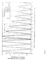
- the interfaces where a silicon on a Molybdenum layer have been deposited are dashed and the interfaces where a molybdenum layer have been deposited on a silicon layer, shown with a dash-dot line.
- the diagram shows that the Bellies of the standing electric wave field generally at a distance from interfaces and here in front of such interfaces, starting from the surface of the multi-layer system are arranged.
- the wave bellies are always the example shown here in front of an interface on a molybdenum layer trained silicon layer arranged.
Landscapes
- Physics & Mathematics (AREA)
- Engineering & Computer Science (AREA)
- Chemical & Material Sciences (AREA)
- Nanotechnology (AREA)
- General Engineering & Computer Science (AREA)
- Crystallography & Structural Chemistry (AREA)
- Theoretical Computer Science (AREA)
- Spectroscopy & Molecular Physics (AREA)
- Mathematical Physics (AREA)
- High Energy & Nuclear Physics (AREA)
- General Physics & Mathematics (AREA)
- Optics & Photonics (AREA)
- Exposure Of Semiconductors, Excluding Electron Or Ion Beam Exposure (AREA)
- Exposure And Positioning Against Photoresist Photosensitive Materials (AREA)
- Formation Of Insulating Films (AREA)
- Physical Vapour Deposition (AREA)
Abstract
Description
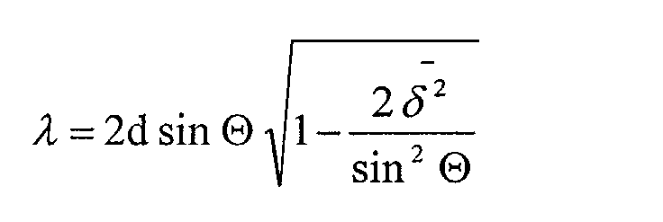
- λ -
- Wellenlänge des Röntgenstrahls
- d -
- Periodendicke der Schichtpaare (= dMo+ dsi)
- -
- Winkel, unter dem der Spiegel reflektiert
- δ -
- Dispersionskorrektur
- Figur 1
- ein Diagramm der Intensität eines stehenden elektrischen Wellenfeldes innerhalb eines Vakuums und innerhalb eines aus Siliziumschichten und Molybdänschichten gebildeten Multischichtsystems.
Claims (12)
- Optisches System mit einer Strahlungsquelle für elektromagnetische Strahlung im extremen ultravioletten Bereich und mindestens einem reflektierenden Element, bei dem auf einem Substrat ein Multischichtsystem mit alternierend angeordneten Schichten aus Mo und Si, als Schichtpaare, ausgebildet ist, dabei die elektromagnetische Strahlung unter einem Winkel auf die Oberfläche des Multischichtsystems gerichtet ist und die Dicke d der Schichtpaare bei der Wellenlänge der elektromagnetischen Strahlung die Braggsche Gleichung erfüllen und zumindest innerhalb des Multischichtsystems ein stehendes elektrisches Wellenfeld auftritt, dadurch gekennzeichnet, dass die Dicken dMo und dsi der Mo- und Si-Schichten so gewählt sind, dass die Knoten des elektrischen Wellenfeldes jeweils unmittelbar an Grenzflächen zwischen solchen Einzelschichten und/oder die Wellenbäuche vor oder nach solchen Grenzflächen angeordnet sind.
- Optisches System nach Anspruch 1, dadurch gekennzeichnet, dass die Grenzflächen durch Zwischenschichten gebildet sind, die zwischen auf Siliziumschichten ausgebildeten Molybdänschichten und/oder zwischen auf Molybdänschichten ausgebildeten Siliziumschichten angeordnet sind.
- Optisches System nach Anspruch 1 oder 2, dadurch gekennzeichnet, dass die Zwischenschichten eine Dicke im Bereich zwischen 0,1 und 3 nm aufweisen.
- Optisches System nach mindestens einem der vorhergehenden Ansprüche, dadurch gekennzeichnet, dass die Zwischenschichten aus eine Silizidbildung verhindernden bzw. behindernden chemischen Elementen oder Verbindungen gebildet sind.
- Optisches System nach mindestens einem der vorhergehenden Ansprüche, dadurch gekennzeichnet, dass Zwischenschichten bei Wellenbäuchen des stehenden Wellenfeldes eine kleinere Dicke aufweisen.
- Optisches System nach mindestens einem der vorhergehenden Ansprüche, dadurch gekennzeichnet, dass zumindest die Zwischenschichten in der Nähe von Wellenbäuchen aus einem für die jeweilige elektromagnetische Strahlung transparenten Element oder Verbindung gebildet sind.
- Optisches System nach mindestens einem der vorhergehenden Ansprüche, dadurch gekennzeichnet, dass die Knoten des stehenden Wellenfeldes an Grenzflächen, bei denen Mo auf Si ausgebildet worden ist, angeordnet sind.
- Optisches System nach Anspruch 7, dadurch gekennzeichnet, dass die Grenzflächen, bei denen Mo auf Si abgeschieden worden ist, keine Zwischenschicht aufweisen.
- Optisches System nach mindestens einem der vorhergehenden Ansprüche, dadurch gekennzeichnet, dass die Zwischenschichten an Knoten des stehenden Wellenfeldes für die jeweilige elektromagnetische Strahlung nicht transparent sind.
- Optisches System nach mindestens einem der vorhergehenden Ansprüche, dadurch gekennzeichnet, dass Zwischenschichten aus B4C, C, Ru, W und/oder Ag gebildet sind.
- Optisches System nach mindestens einem der vorhergehenden Ansprüche, dadurch gekennzeichnet, dass das Multischichtsystem mit mindestens zehn aus Mo- und Si-Schichten bestehenden Schichtpaaren gebildet ist.
- Optisches System nach mindestens einem der vorhergehenden Ansprüche, dadurch gekennzeichnet, dass das reflektierende Element zur Fokussierung und/oder Strahlformung der elektromagnetischen Strahlung eine gewölbte Oberfläche aufweist.
Applications Claiming Priority (4)
| Application Number | Priority Date | Filing Date | Title |
|---|---|---|---|
| DE10210422 | 2002-03-04 | ||
| DE10210422 | 2002-03-04 | ||
| DE10221116A DE10221116B3 (de) | 2002-03-04 | 2002-05-03 | Optisches System mit einer Strahlungsquelle für elektromagnetische Strahlung im extremen ultravioletten Bereich und einem reflektierenden Element |
| DE10221116 | 2002-05-03 |
Publications (2)
| Publication Number | Publication Date |
|---|---|
| EP1351258A1 true EP1351258A1 (de) | 2003-10-08 |
| EP1351258B1 EP1351258B1 (de) | 2005-11-16 |
Family
ID=28042826
Family Applications (1)
| Application Number | Title | Priority Date | Filing Date |
|---|---|---|---|
| EP03400006A Expired - Lifetime EP1351258B1 (de) | 2002-03-04 | 2003-03-03 | Methode zur Auswahl der Schichtdicken eines reflektierenden Elements für elektromagnetische Strahlung im extremen ultravioletten Bereich |
Country Status (3)
| Country | Link |
|---|---|
| EP (1) | EP1351258B1 (de) |
| AT (1) | ATE310311T1 (de) |
| DE (1) | DE50301645D1 (de) |
Cited By (2)
| Publication number | Priority date | Publication date | Assignee | Title |
|---|---|---|---|---|
| WO2005091076A3 (en) * | 2004-03-05 | 2007-01-18 | Zeiss Carl Smt Ag | Methods for manufacturing reflective optical elements |
| WO2020011853A1 (de) * | 2018-07-11 | 2020-01-16 | Carl Zeiss Smt Gmbh | Reflektives optisches element |
Citations (4)
| Publication number | Priority date | Publication date | Assignee | Title |
|---|---|---|---|---|
| US5086443A (en) * | 1990-08-03 | 1992-02-04 | The United States Of America As Represented By The United States Department Of Energy | Background-reducing x-ray multilayer mirror |
| US5307395A (en) * | 1992-09-30 | 1994-04-26 | The United States Of America As Represented By The Secretary Of The Navy | Low-damage multilayer mirror for the soft X-ray region |
| EP1065568A2 (de) * | 1999-07-02 | 2001-01-03 | Asm Lithography B.V. | EUV-lithographische Projektionsvorrichtung mit einem optischen Element mit Deckschicht |
| US6295164B1 (en) * | 1998-09-08 | 2001-09-25 | Nikon Corporation | Multi-layered mirror |
-
2003
- 2003-03-03 AT AT03400006T patent/ATE310311T1/de active
- 2003-03-03 EP EP03400006A patent/EP1351258B1/de not_active Expired - Lifetime
- 2003-03-03 DE DE50301645T patent/DE50301645D1/de not_active Expired - Fee Related
Patent Citations (4)
| Publication number | Priority date | Publication date | Assignee | Title |
|---|---|---|---|---|
| US5086443A (en) * | 1990-08-03 | 1992-02-04 | The United States Of America As Represented By The United States Department Of Energy | Background-reducing x-ray multilayer mirror |
| US5307395A (en) * | 1992-09-30 | 1994-04-26 | The United States Of America As Represented By The Secretary Of The Navy | Low-damage multilayer mirror for the soft X-ray region |
| US6295164B1 (en) * | 1998-09-08 | 2001-09-25 | Nikon Corporation | Multi-layered mirror |
| EP1065568A2 (de) * | 1999-07-02 | 2001-01-03 | Asm Lithography B.V. | EUV-lithographische Projektionsvorrichtung mit einem optischen Element mit Deckschicht |
Non-Patent Citations (2)
| Title |
|---|
| BAJT S ET AL: "IMPROVED REFLECTANCE AND STABILITY OF MO/SI MULTILAYERS", PROCEEDINGS OF THE SPIE, SPIE, BELLINGHAM, VA, US, vol. 4506, 31 July 2001 (2001-07-31), pages 65 - 75, XP008017154 * |
| TAKENAKA H ET AL: "DESIGN AND FABRICATION OF HIGHLY HEAT-RESISTANT MO/SI MULTILAYER SOFT X-RAY MIRRORS WITH INTERLEAVED BARRIER LAYERS", JOURNAL OF SYNCHROTRON RADIATION, XX, XX, vol. 5, no. PART 3, 4 August 1997 (1997-08-04), pages 708 - 710, XP008007468, ISSN: 0909-0495 * |
Cited By (3)
| Publication number | Priority date | Publication date | Assignee | Title |
|---|---|---|---|---|
| WO2005091076A3 (en) * | 2004-03-05 | 2007-01-18 | Zeiss Carl Smt Ag | Methods for manufacturing reflective optical elements |
| WO2020011853A1 (de) * | 2018-07-11 | 2020-01-16 | Carl Zeiss Smt Gmbh | Reflektives optisches element |
| US11520087B2 (en) | 2018-07-11 | 2022-12-06 | Carl Zeiss Smt Gmbh | Reflective optical element |
Also Published As
| Publication number | Publication date |
|---|---|
| DE50301645D1 (de) | 2005-12-22 |
| EP1351258B1 (de) | 2005-11-16 |
| ATE310311T1 (de) | 2005-12-15 |
Similar Documents
| Publication | Publication Date | Title |
|---|---|---|
| DE102004062289B4 (de) | Thermisch stabiler Multilayer-Spiegel für den EUV-Spektralbereich | |
| DE102010019256B4 (de) | Zonenoptimierte Spiegel, optische Systeme mit solchen Spiegeln und Verfahren zur Herstellung solcher Spiegel | |
| DE102008007387A1 (de) | Reflektives optisches Element für EUV-Lithographievorrichtungen | |
| DE102018211499A1 (de) | Reflektives optisches Element und Verfahren zum Herstellen eines reflektiven optischen Elements | |
| EP3491468B1 (de) | Reflektives optisches element für die euv-lithographie | |
| DE102017213181A1 (de) | Optische Anordnung für EUV-Strahlung mit einer Abschirmung zum Schutz vor der Ätzwirkung eines Plasmas | |
| DE102014204660A1 (de) | Spiegel, insbesondere für eine mikrolithographische Projektionsbelichtungsanlage | |
| DE102007051671A1 (de) | Abbildende Optik sowie Projektionsbelichtungsanlage für die Mikrolithographie mit einer derartigen abbildenden Optik | |
| DE102011079933A1 (de) | Optisches Element für die UV- oder EUV-Lithographie | |
| DE102018211980A1 (de) | Reflektives optisches Element | |
| DE102015213273A1 (de) | Spiegel, insbesondere für eine mikrolithographische Projektionsbelichtungsanlage | |
| WO2007090364A2 (de) | Thermisch stabiler multilayer-spiegel für den euv-spektralbereich | |
| DE102012203633A1 (de) | Spiegel für den EUV-Wellenlängenbereich, Herstellungsverfahren für einen solchen Spiegel und Projektionsbelichtungsanlage mit einem solchen Spiegel | |
| EP3589989A1 (de) | Verfahren zur korrektur eines reflektiven optischen elements für den wellenlängenbereich von 5 nm bis 20 nm | |
| EP1351258B1 (de) | Methode zur Auswahl der Schichtdicken eines reflektierenden Elements für elektromagnetische Strahlung im extremen ultravioletten Bereich | |
| DE10221116B3 (de) | Optisches System mit einer Strahlungsquelle für elektromagnetische Strahlung im extremen ultravioletten Bereich und einem reflektierenden Element | |
| DE10254026B4 (de) | Reflektor für Röntgenstrahlung | |
| EP2824487A1 (de) | Reflektives optisches Element für streifenden Einfall im EUV-Wellenlängenbereich | |
| DE102016209273A1 (de) | Spiegel für den euv-wellenlängenbereich | |
| WO2004097467A1 (de) | Reflektives optisches element, optisches system und euv-lithographievorrichtung | |
| DE102015208705A1 (de) | Kombinierter reflektor und filter für licht unterschiedlicher wellenlängen | |
| WO2023194355A1 (de) | Reflektives optisches element für eine wellenlänge im extrem ultravioletten wellenlängenbereich | |
| DE102015203604B4 (de) | Schichtaufbau für mehrschichtige Laue-Linsen bzw. zirkulare Multischicht-Zonenplatten | |
| DE10241330A1 (de) | Spiegelelement für die Reflektion von Röntgenstrahlen | |
| DE102016213839A1 (de) | Spiegel für ein mikrolithographisches Projektionsbelichtungssystem und Verfahren zur Bearbeitung eines Spiegels |
Legal Events
| Date | Code | Title | Description |
|---|---|---|---|
| PUAI | Public reference made under article 153(3) epc to a published international application that has entered the european phase |
Free format text: ORIGINAL CODE: 0009012 |
|
| AK | Designated contracting states |
Kind code of ref document: A1 Designated state(s): AT BE BG CH CY CZ DE DK EE ES FI FR GB GR HU IE IT LI LU MC NL PT RO SE SI SK TR |
|
| AX | Request for extension of the european patent |
Extension state: AL LT LV MK |
|
| RAP1 | Party data changed (applicant data changed or rights of an application transferred) |
Owner name: FRAUNHOFER-GESELLSCHAFT ZUR FOERDERUNG DERANGEWAND |
|
| 17P | Request for examination filed |
Effective date: 20040226 |
|
| 17Q | First examination report despatched |
Effective date: 20040426 |
|
| AKX | Designation fees paid |
Designated state(s): AT BE BG CH CY CZ DE DK EE ES FI FR GB GR HU IE IT LI LU MC NL PT RO SE SI SK TR |
|
| GRAP | Despatch of communication of intention to grant a patent |
Free format text: ORIGINAL CODE: EPIDOSNIGR1 |
|
| RTI1 | Title (correction) |
Free format text: METHOD OF SELECTING LAYER THICKNESSES OF A REFLECTIVE ELEMENT FOR EXTREME ULTRA VIOLET RADIATION |
|
| GRAS | Grant fee paid |
Free format text: ORIGINAL CODE: EPIDOSNIGR3 |
|
| GRAA | (expected) grant |
Free format text: ORIGINAL CODE: 0009210 |
|
| AK | Designated contracting states |
Kind code of ref document: B1 Designated state(s): AT BE BG CH CY CZ DE DK EE ES FI FR GB GR HU IE IT LI LU MC NL PT RO SE SI SK TR |
|
| PG25 | Lapsed in a contracting state [announced via postgrant information from national office to epo] |
Ref country code: IT Free format text: LAPSE BECAUSE OF FAILURE TO SUBMIT A TRANSLATION OF THE DESCRIPTION OR TO PAY THE FEE WITHIN THE PRESCRIBED TIME-LIMIT;WARNING: LAPSES OF ITALIAN PATENTS WITH EFFECTIVE DATE BEFORE 2007 MAY HAVE OCCURRED AT ANY TIME BEFORE 2007. THE CORRECT EFFECTIVE DATE MAY BE DIFFERENT FROM THE ONE RECORDED. Effective date: 20051116 Ref country code: SK Free format text: LAPSE BECAUSE OF FAILURE TO SUBMIT A TRANSLATION OF THE DESCRIPTION OR TO PAY THE FEE WITHIN THE PRESCRIBED TIME-LIMIT Effective date: 20051116 Ref country code: CZ Free format text: LAPSE BECAUSE OF FAILURE TO SUBMIT A TRANSLATION OF THE DESCRIPTION OR TO PAY THE FEE WITHIN THE PRESCRIBED TIME-LIMIT Effective date: 20051116 Ref country code: FI Free format text: LAPSE BECAUSE OF FAILURE TO SUBMIT A TRANSLATION OF THE DESCRIPTION OR TO PAY THE FEE WITHIN THE PRESCRIBED TIME-LIMIT Effective date: 20051116 Ref country code: RO Free format text: LAPSE BECAUSE OF FAILURE TO SUBMIT A TRANSLATION OF THE DESCRIPTION OR TO PAY THE FEE WITHIN THE PRESCRIBED TIME-LIMIT Effective date: 20051116 Ref country code: SI Free format text: LAPSE BECAUSE OF FAILURE TO SUBMIT A TRANSLATION OF THE DESCRIPTION OR TO PAY THE FEE WITHIN THE PRESCRIBED TIME-LIMIT Effective date: 20051116 Ref country code: IE Free format text: LAPSE BECAUSE OF FAILURE TO SUBMIT A TRANSLATION OF THE DESCRIPTION OR TO PAY THE FEE WITHIN THE PRESCRIBED TIME-LIMIT Effective date: 20051116 |
|
| REG | Reference to a national code |
Ref country code: GB Ref legal event code: FG4D Free format text: NOT ENGLISH |
|
| REG | Reference to a national code |
Ref country code: CH Ref legal event code: EP |
|
| REG | Reference to a national code |
Ref country code: IE Ref legal event code: FG4D Free format text: LANGUAGE OF EP DOCUMENT: GERMAN |
|
| REF | Corresponds to: |
Ref document number: 50301645 Country of ref document: DE Date of ref document: 20051222 Kind code of ref document: P |
|
| PG25 | Lapsed in a contracting state [announced via postgrant information from national office to epo] |
Ref country code: DK Free format text: LAPSE BECAUSE OF FAILURE TO SUBMIT A TRANSLATION OF THE DESCRIPTION OR TO PAY THE FEE WITHIN THE PRESCRIBED TIME-LIMIT Effective date: 20060216 Ref country code: GR Free format text: LAPSE BECAUSE OF FAILURE TO SUBMIT A TRANSLATION OF THE DESCRIPTION OR TO PAY THE FEE WITHIN THE PRESCRIBED TIME-LIMIT Effective date: 20060216 Ref country code: BG Free format text: LAPSE BECAUSE OF FAILURE TO SUBMIT A TRANSLATION OF THE DESCRIPTION OR TO PAY THE FEE WITHIN THE PRESCRIBED TIME-LIMIT Effective date: 20060216 |
|
| PG25 | Lapsed in a contracting state [announced via postgrant information from national office to epo] |
Ref country code: ES Free format text: LAPSE BECAUSE OF FAILURE TO SUBMIT A TRANSLATION OF THE DESCRIPTION OR TO PAY THE FEE WITHIN THE PRESCRIBED TIME-LIMIT Effective date: 20060227 |
|
| REG | Reference to a national code |
Ref country code: CH Ref legal event code: NV Representative=s name: TROESCH SCHEIDEGGER WERNER AG |
|
| REG | Reference to a national code |
Ref country code: SE Ref legal event code: TRGR |
|
| GBT | Gb: translation of ep patent filed (gb section 77(6)(a)/1977) |
Effective date: 20060227 |
|
| PG25 | Lapsed in a contracting state [announced via postgrant information from national office to epo] |
Ref country code: MC Free format text: LAPSE BECAUSE OF NON-PAYMENT OF DUE FEES Effective date: 20060331 Ref country code: LU Free format text: LAPSE BECAUSE OF NON-PAYMENT OF DUE FEES Effective date: 20060331 Ref country code: BE Free format text: LAPSE BECAUSE OF NON-PAYMENT OF DUE FEES Effective date: 20060331 |
|
| PG25 | Lapsed in a contracting state [announced via postgrant information from national office to epo] |
Ref country code: PT Free format text: LAPSE BECAUSE OF FAILURE TO SUBMIT A TRANSLATION OF THE DESCRIPTION OR TO PAY THE FEE WITHIN THE PRESCRIBED TIME-LIMIT Effective date: 20060417 |
|
| PG25 | Lapsed in a contracting state [announced via postgrant information from national office to epo] |
Ref country code: HU Free format text: LAPSE BECAUSE OF FAILURE TO SUBMIT A TRANSLATION OF THE DESCRIPTION OR TO PAY THE FEE WITHIN THE PRESCRIBED TIME-LIMIT Effective date: 20060517 |
|
| REG | Reference to a national code |
Ref country code: IE Ref legal event code: FD4D |
|
| ET | Fr: translation filed | ||
| PLBE | No opposition filed within time limit |
Free format text: ORIGINAL CODE: 0009261 |
|
| STAA | Information on the status of an ep patent application or granted ep patent |
Free format text: STATUS: NO OPPOSITION FILED WITHIN TIME LIMIT |
|
| PG25 | Lapsed in a contracting state [announced via postgrant information from national office to epo] |
Ref country code: DE Free format text: LAPSE BECAUSE OF NON-PAYMENT OF DUE FEES Effective date: 20061003 |
|
| 26N | No opposition filed |
Effective date: 20060817 |
|
| BERE | Be: lapsed |
Owner name: FRAUNHOFER-GESELLSCHAFT ZUR FORDERUNG DER ANGEWAN Effective date: 20060331 |
|
| PG25 | Lapsed in a contracting state [announced via postgrant information from national office to epo] |
Ref country code: EE Free format text: LAPSE BECAUSE OF FAILURE TO SUBMIT A TRANSLATION OF THE DESCRIPTION OR TO PAY THE FEE WITHIN THE PRESCRIBED TIME-LIMIT Effective date: 20051116 |
|
| PG25 | Lapsed in a contracting state [announced via postgrant information from national office to epo] |
Ref country code: TR Free format text: LAPSE BECAUSE OF FAILURE TO SUBMIT A TRANSLATION OF THE DESCRIPTION OR TO PAY THE FEE WITHIN THE PRESCRIBED TIME-LIMIT Effective date: 20051116 |
|
| PG25 | Lapsed in a contracting state [announced via postgrant information from national office to epo] |
Ref country code: CY Free format text: LAPSE BECAUSE OF FAILURE TO SUBMIT A TRANSLATION OF THE DESCRIPTION OR TO PAY THE FEE WITHIN THE PRESCRIBED TIME-LIMIT Effective date: 20051116 |
|
| REG | Reference to a national code |
Ref country code: FR Ref legal event code: PLFP Year of fee payment: 14 |
|
| REG | Reference to a national code |
Ref country code: FR Ref legal event code: PLFP Year of fee payment: 15 |
|
| REG | Reference to a national code |
Ref country code: FR Ref legal event code: PLFP Year of fee payment: 16 |
|
| PGFP | Annual fee paid to national office [announced via postgrant information from national office to epo] |
Ref country code: GB Payment date: 20220324 Year of fee payment: 20 Ref country code: CH Payment date: 20220324 Year of fee payment: 20 Ref country code: AT Payment date: 20220318 Year of fee payment: 20 |
|
| PGFP | Annual fee paid to national office [announced via postgrant information from national office to epo] |
Ref country code: SE Payment date: 20220324 Year of fee payment: 20 Ref country code: NL Payment date: 20220322 Year of fee payment: 20 Ref country code: FR Payment date: 20220322 Year of fee payment: 20 |
|
| REG | Reference to a national code |
Ref country code: NL Ref legal event code: MK Effective date: 20230302 |
|
| REG | Reference to a national code |
Ref country code: CH Ref legal event code: PL |
|
| REG | Reference to a national code |
Ref country code: GB Ref legal event code: PE20 Expiry date: 20230302 |
|
| REG | Reference to a national code |
Ref country code: AT Ref legal event code: MK07 Ref document number: 310311 Country of ref document: AT Kind code of ref document: T Effective date: 20230303 |
|
| REG | Reference to a national code |
Ref country code: SE Ref legal event code: EUG |
|
| PG25 | Lapsed in a contracting state [announced via postgrant information from national office to epo] |
Ref country code: GB Free format text: LAPSE BECAUSE OF EXPIRATION OF PROTECTION Effective date: 20230302 |