EP1349272A1 - High frequency low-pass filter - Google Patents
High frequency low-pass filter Download PDFInfo
- Publication number
- EP1349272A1 EP1349272A1 EP01272825A EP01272825A EP1349272A1 EP 1349272 A1 EP1349272 A1 EP 1349272A1 EP 01272825 A EP01272825 A EP 01272825A EP 01272825 A EP01272825 A EP 01272825A EP 1349272 A1 EP1349272 A1 EP 1349272A1
- Authority
- EP
- European Patent Office
- Prior art keywords
- section
- lpf
- frequency
- hpf
- band
- Prior art date
- Legal status (The legal status is an assumption and is not a legal conclusion. Google has not performed a legal analysis and makes no representation as to the accuracy of the status listed.)
- Withdrawn
Links
Images


Classifications
-
- H—ELECTRICITY
- H03—ELECTRONIC CIRCUITRY
- H03H—IMPEDANCE NETWORKS, e.g. RESONANT CIRCUITS; RESONATORS
- H03H7/00—Multiple-port networks comprising only passive electrical elements as network components
- H03H7/01—Frequency selective two-port networks
- H03H7/17—Structural details of sub-circuits of frequency selective networks
- H03H7/1741—Comprising typical LC combinations, irrespective of presence and location of additional resistors
- H03H7/1758—Series LC in shunt or branch path
-
- H—ELECTRICITY
- H03—ELECTRONIC CIRCUITRY
- H03H—IMPEDANCE NETWORKS, e.g. RESONANT CIRCUITS; RESONATORS
- H03H7/00—Multiple-port networks comprising only passive electrical elements as network components
- H03H7/01—Frequency selective two-port networks
- H03H7/0115—Frequency selective two-port networks comprising only inductors and capacitors
-
- H—ELECTRICITY
- H03—ELECTRONIC CIRCUITRY
- H03H—IMPEDANCE NETWORKS, e.g. RESONANT CIRCUITS; RESONATORS
- H03H7/00—Multiple-port networks comprising only passive electrical elements as network components
- H03H7/01—Frequency selective two-port networks
- H03H7/17—Structural details of sub-circuits of frequency selective networks
- H03H7/1741—Comprising typical LC combinations, irrespective of presence and location of additional resistors
- H03H7/1766—Parallel LC in series path
-
- H—ELECTRICITY
- H03—ELECTRONIC CIRCUITRY
- H03H—IMPEDANCE NETWORKS, e.g. RESONANT CIRCUITS; RESONATORS
- H03H7/00—Multiple-port networks comprising only passive electrical elements as network components
- H03H7/46—Networks for connecting several sources or loads, working on different frequencies or frequency bands, to a common load or source
Definitions
- the present invention relates to a high frequency low-pass filter (LPF) employed in mobile communication devices such as a cellular phone.
- LPF high frequency low-pass filter
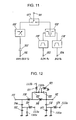
- Fig. 11 is a circuit block diagram of a front end of a dual-band cellular phone usable in both Global System for Mobile Communication (GSM) and Digital Cellular System (DCS).
- GSM Global System for Mobile Communication
- DCS Digital Cellular System
- a transmission signal, applicable to both GSM and DCS, produced in a cellular phone runs through transmitting terminal 102 and is amplified by power amplifier (hereinafter referred to as PA) 105, then the signal is fed into high frequency low-pass filter (hereinafter referred to as LPF) 106.
- PA power amplifier
- LPF high frequency low-pass filter
- This high powered transmission signal undergoes LPF 106 as well as transmit/receive switch 107, and arrives at antenna terminal 101.
- a receipt signal applicable to both GSM and DCS, received by an antenna runs through antenna terminal 101, switch 107, and is fed into diplexer (branching circuit) 108.
- the receipt signal is branched into a signal of GSM and a signal of DCS, and both signals undergo respective receiving filters 109 and 110 before arriving at respective receiving terminals 103 and 104.
- a critical point is how to restrain harmonics component developed at the high power amplification done in the PA.
- a normal LPF of which cut-off frequency is simply higher than the DCS band is provided, second harmonics of GSM overlap with a transmission band of DCS.
- the second harmonics of GSM cannot be restrained. Therefore, a cut-off frequency of LPF 106 should be switched to an adequate value responsive to GSM transmission and DCS transmission.
- a conventional LPF is formed of a ⁇ type C-L-C filter.
- These C, L and C comprise a series circuit formed of capacitors 114, 115, another series circuit formed of inductor 118, 119, and still another series circuit formed of capacitors 116, 117 respectively.
- the conventional LPF has input terminal 111 and output terminal 112.
- a direct current (DC) is applied to control terminals 113a and 113B for turning on/off diodes 120a and 120b respectively.
- Inductor 121 and capacitor 122 work as a choke coil and a DC-blocking capacitor respectively.
- the present invention addresses the problems discussed above, and aims to provide a downsized and a sophisticated LPF of low cost as well as low insertion loss. For this purpose, a number of switching diodes is minimized. Further, it is not only switching a cut-off frequency of the LPF, but also newly providing the LPF with a high-pass filter (HPF section) in a high frequency band or a band pass filter (BPF section).
- HPF section high-pass filter
- BPF section band pass filter
- the LPF of the present invention comprises the following elements:
- the present invention includes the following aspects:
- Fig. 1 is a block circuit diagram of an LPF in accordance with the first embodiment.
- a transmission filter of a dual-band cellular phone usable both in GSM and DCS includes input terminal 1 and output terminal 2.
- HPF section 3 and LPF section 4 allow a signal of DCS band and a signal of GSM band to pass therethrough respectively.
- a transmission frequency of DCS is 1.710 - 1.785 MHz, and that of GSM is 880 - 915 MHz.
- An on/off switch is added to HPF section 3 of the LPF so that the LPF also works as a filter for rejecting harmonics component of the dual-band cellular phone.
- the LPF stays in a switch on status during a DCS transmission so that a DCS transmission signal can pass through with a low insertion loss.
- the LPF stays in switch-off status in order to block secondary harmonics component of the GSM transmission signal from passing through HPF section 3.
- a fundamental wave can pass through LPF section 4 with a low insertion loss.
- This structure allows the LPF to output a GSM transmission signal, of which secondary harmonics are restrained; during the GSM transmission, as well as output a DCS transmission signal during the DCS transmission.
- a desirable LPF is obtainable.
- an LPF shown in a block circuit diagram of Fig. 2 is effective.
- second LPF section 5 is coupled in series between output terminal 2 and HPF section 3, LPF section 4. This structure allows second LPF section 5 to restrain a second and onward harmonics component of DCS transmission signals as well as a third and onward harmonics component of GSM transmission signals.
- Fig. 3 shows an actual circuit of the LPF based on the block diagram shown in Fig. 2.
- a circuit constant of a parallel circuit formed of capacitor 8 and inductor 13 is prepared so as to parallel-resonate in a DCS transmission band.
- a circuit constant of a series circuit formed of capacitor 9 and inductor 14 is prepared to series-resonate in a GSM transmission band.
- the parallel resonance circuit formed of capacitor 8 and inductor 13 parallel-resonates in the DCS transmission band. Therefore, a circuit between terminals 1 and 2' works as a HPF section of T-type C-L-C, and a DCS band input-signal arrived at terminal 1 can pass through the LPF without disturbing an impedance matching.
- a parallel-resonant circuit formed of capacitor 11 and inductor 15 is provided in the second LPF section coupled between terminals 2 - 2', so that the frequency characteristic of the LPF includes an attenuation pole. (the characteristic shows a sharp attenuation at a certain frequency) As such, the LPF can further restrain the harmonics component efficiently.
- a series-resonant circuit formed of an inductor connected to capacitor 10, 12 respectively in series and in shunt can produce a similar advantage.
- the LPF needs only one single diode in its circuit, which can be thus simply constructed without a complicated control system.
- the circuit therefore eventually needs a small number of components.
- a sophisticated LPF with a simple structure can obtain characteristics of a low insertion loss and characteristics of efficiently restraining harmonics component.
- Fig. 4 shows a detailed circuit diagram in accordance with the second exemplary embodiment.
- capacitors 19 - 25 and inductors 26-30 are prepared.
- a circuit constant of a series circuit formed of capacitor 21 and inductor 29 is set so as to series-resonate in the DCS transmission band.
- a circuit constant of a series circuit formed of capacitor 22 and inductor 28 is set so as to series-resonate in the GSM transmission band.
- capacitor 21 and inductor 29 series-resonates in the DCS transmission band. Therefore, a circuit between terminals 1 and 2' works as an HPF section of five-element and ⁇ -type L-C -L-C-L, and a DCS band input-signal arrived at terminal 1 can pass through the LPF without disturbing an impedance matching.
- Fig. 5 and Fig. 6 show the passing characteristics of the LPF in accordance with the second embodiment.
- attenuation amounts M1 - M4 at frequency I1 are shown.
- Fig. 5 shows the passing characteristics during the GSM transmission, where diode 17 is in an ON status.
- Fig. 6 shows the passing characteristics during the DCS transmission, where diode 17 is in an OFF status.
- Attenuation amounts M1 -M4 at frequency I1 are shown here. According to these passing characteristics, passing loss becomes smaller, and harmonics are substantially restrained.
- a parallel-resonant circuit formed of capacitor 25 and inductor 30 is provided in the second LPF section coupled between terminals 2 - 2', so that the frequency characteristic of the LPF includes an attenuation pole. As such, the LPF can further restrain the harmonics component efficiently.
- a series-resonant circuit formed of an inductor connected to capacitor 23, 24 in series and in shunt can produce a similar advantage.
- second LPF section 5 is omitted, and HPF section 3 is replaced with band pass filter (BPF) 31 as shown in Fig. 7.
- BPF band pass filter
- third LPF section 32 is cascade-connected to first LPF section 4 for restraining the harmonics component more efficiently.
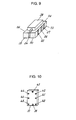
- Fig. 9 is a perspective view of a structure of an object in accordance with the third exemplary embodiment of the present invention.
- the circuit components of the LPF in accordance with this embodiment are disposed as an electrode pattern (not shown) in dielectric laminated body 33, and diode 38 is mounted on a surface of laminated body 33, thereby downsizing the LPF.
- Outer terminals of the LPF (in Fig. 9, only outer terminals 34 - 37 are shown can be prepared on a side face of laminated body 33. Further, it is desirable to prepare input and output terminals on the faces opposite to each other in order to improve an attenuation characteristic of an undesired signal, so that more sophistication of the LPF can be expected.
- an output terminal is desirably prepared on face 54, or vice versa.
- an output terminal is desirably prepared on face 56.
- the attenuation characteristic improves at a greater distance between an input terminal and an output terminal.
- terminal 41 is assigned to an input terminal
- terminals 45, 44 or 46 instead of terminal 40 or 42 is desirably assigned to an output terminal.
- a combination of terminals 39 and 43, terminals 40 and 44, or terminals 42 and 46 is desirable as a combination of input and output terminals. Because one of these combinations extends a distance between the input and output terminals, so that sufficient electrical isolation is provided between the input and output terminals. As a result, an excellent attenuation characteristic can be expected.
- An HPF section or a BPF section is connected with a first LPF section in parallel, and further, the HPF section or the BPF section is connected to a changeover switch that changes over the pass band to a rejection band.
- This structure allows the switch to activate to restrain the second harmonics component from passing the HPF section or the BPF section when a fundamental wave is input to the LPF as a high power signal supposed to pass through a first LPF section.
- the present invention needs only one single changeover switch, thus a compact and sophisticated LPF is obtainable, and the LPF incurs only a low insertion loss and has an excellent harmonics suppression characteristic.
- the LPF can be widely used as a dual-band transmission filter of dual-band cellular phones.
Landscapes
- Engineering & Computer Science (AREA)
- Power Engineering (AREA)
- Filters And Equalizers (AREA)
- Transceivers (AREA)
Abstract
Description
Claims (21)
- A low pass filter (LPF) for filtering a signal in a high frequency band, said LPF comprising:'wherein an input section of said HPF section is coupled with an input section of said first LPF section, and .a high pass filter (HPF) section for filtering an input signala first LPF section for filtering the input signal anda changeover switch for changing a pass band of said HPF section to a rejection band,
wherein the output section of said HPF section is coupled with an output section of said first LPF section. - The LPF of claim 1 further comprising a second LPF section that is cascade-coupled with said first LPF section.
- The LPF of claim 1 or claim 2, wherein said HPF section is assembled with a first capacitor, a series-resonant circuit formed of a first inductor and a second capacitor, and a third capacitor in T-connection,
wherein a resonant frequency of the series-resonant circuit is set at a frequency within a pass band of said first LPF section;
wherein said first LPF section is formed of a parallel-resonant circuit assembled with a second inductor and a fourth capacitor, and
wherein a resonant frequency of the parallel-resonant circuit is set at a frequency within a pass band of said HPF section. - The LPF of claim 1 or claim 2,
wherein said HPF section is assembled with a fifth capacitor, a first series-resonant circuit formed of a third inductor and a sixth capacitor, and a seventh capacitor in T-connection;
wherein a resonant frequency of the series-resonant circuit is set at a frequency within a pass band of said first LPF section
wherein said first LPF section is assembled with a fourth inductor, a second series-resonant circuit formed of a fifth inductor and an eighth capacitor, and a sixth inductor in T-connection; and
wherein a resonant frequency of the second series-resonant circuit is set at a frequency within the pass band of said HPF section. - A low pass filter (LPF) for filtering a signal in a high frequency band, said LPF comprising:wherein an input section of said BPF section is coupled with an input section of said first LPF section, anda band pass filter (BPF) section for filtering an input signalsa first LPF section for filtering the input signal anda changeover switch for changing a pass band of said BPF section to a rejection band,
wherein the output section of said BPF section is coupled with an output section of said first LPF section. - The LPF of claim 5 further comprising a second LPF section that is cascade-coupled with said first LPF section.
- The LPF of claim 1 or claim 2, wherein a transmission characteristic of said HPF section includes an attenuation pole at a frequency within a pass band of said first LPF section.
- The LPF of claim 5 or claim 6, wherein a transmission characteristic of said BPF section includes an attenuation pole at a frequency within a pass band of said first LPF section.
- The LPF of claim 1 or claim 2, wherein a transmission characteristic of said first LPF section includes an attenuation pole at a frequency within a pass band of said HPF section.
- The LPF of claim 5 or claim 6, wherein a transmission characteristic of said first LPF section includes an attenuation pole at a frequency within a pass band of said BPF section.
- The LPF of claims 3, 4 or 7,
wherein a series-resonant circuit coupled between a main path of said HPF section and a ground resonates at a frequency within a pass band of said first LPF section, so that said HPF section produces an attenuation pole at the frequency and
wherein a diode coupled with the resonant circuit in parallel turns to be conductive, so that a pass band of said HPF section is switched to a rejection band. - The LPF of claims 5, 6 or 8,
wherein a series-resonant circuit coupled between a main path of said BPF section and a ground resonates at a frequency within a pass band of said first LPF section, so that said BPF section produces an attenuation pole at the frequency and
wherein a diode coupled with the resonant circuit in parallel turns to be conductive, so that a pass band of said BPF section is switched to a rejection band. - The LPF of claim 1, wherein a frequency of the pass band of said HPF section is approx. twice as much as a frequency of a pass band of said first LPF section.
- The LPF of claim 5, wherein a frequency of the pass band of said BPF section is approx. twice as much as a frequency of a pass band of said first LPF section.
- The LPF of claim 2, wherein the second LPF section includes an attenuation pole in a frequency band higher than a frequency of a signal passing through-said HPF section and said first LPF section.
- The LPF of claim 6, wherein the second LPF section includes an attenuation pole in a frequency band higher than a frequency of a signal passing through said BPF section and said first LPF section.
- The LPF of claim 1 or claim 2, wherein one of parts and entire of said HPF section and said first LPF section are formed in a dielectric laminated body, and said switch is mounted on a surface layer of the laminated body.
- The LPF of claim 11, wherein one of parts and entire of said HPF section and said first LPF section are formed in a dielectric laminated body, and the diode is mounted on a surface layer of the laminated body.
- The LPF of claim 5 or claim 6, wherein one of parts and entire of said first LPF section is formed in a dielectric laminated body, and said switch is mounted on a surface layer of the laminated body.
- The LPF of claim 12, wherein one of parts and entire of said BPF section and said first LPF section are formed in a dielectric laminated body, and the diode is mounted on a surface layer of the laminated body.
- The LPF of claims 17 or 19, wherein an input terminal and an output terminal are disposed on side faces opposite to each other of the laminated body, or on bottom faces opposite to each other of the laminated body.
Applications Claiming Priority (3)
| Application Number | Priority Date | Filing Date | Title |
|---|---|---|---|
| JP2000400452A JP2002204135A (en) | 2000-12-28 | 2000-12-28 | High frequency low pass filter |
| JP2000400452 | 2000-12-28 | ||
| PCT/JP2001/011177 WO2002054591A1 (en) | 2000-12-28 | 2001-12-20 | High frequency low-pass filter |
Publications (2)
| Publication Number | Publication Date |
|---|---|
| EP1349272A1 true EP1349272A1 (en) | 2003-10-01 |
| EP1349272A4 EP1349272A4 (en) | 2006-02-01 |
Family
ID=18865043
Family Applications (1)
| Application Number | Title | Priority Date | Filing Date |
|---|---|---|---|
| EP01272825A Withdrawn EP1349272A4 (en) | 2000-12-28 | 2001-12-20 | HIGH FREQUENCY PASS-LOW FILTER |
Country Status (4)
| Country | Link |
|---|---|
| US (1) | US6895228B2 (en) |
| EP (1) | EP1349272A4 (en) |
| JP (1) | JP2002204135A (en) |
| WO (1) | WO2002054591A1 (en) |
Cited By (4)
| Publication number | Priority date | Publication date | Assignee | Title |
|---|---|---|---|---|
| EP1443641A1 (en) * | 2003-01-13 | 2004-08-04 | Thomson Licensing S.A. | Switchable tuneable bandpass filter with optimized frequency response |
| CN101951239A (en) * | 2010-10-18 | 2011-01-19 | 江苏贝孚德通讯科技股份有限公司 | Composite filter with steep attenuation characteristic |
| CN104993799A (en) * | 2015-07-20 | 2015-10-21 | 天津大学 | Flexible radio frequency strain adjustable passive high-pass filter and manufacturing method thereof |
| CN105763166A (en) * | 2016-04-25 | 2016-07-13 | 天津大学 | Flexible radio frequency strain adjustable passive low pass filter, and manufacturing and measuring method thereof |
Families Citing this family (9)
| Publication number | Priority date | Publication date | Assignee | Title |
|---|---|---|---|---|
| US6417933B1 (en) | 1996-12-26 | 2002-07-09 | Lucent Technologies Inc. | Teleconferencing and facsimile communications system and method |
| WO2004073193A1 (en) * | 2003-02-14 | 2004-08-26 | Hitachi Metals, Ltd. | Switch circuit and composite high frequency elements |
| TWI279980B (en) * | 2003-04-22 | 2007-04-21 | Delta Electronics Inc | Switchable high frequency bandpass filter |
| US7680477B2 (en) * | 2004-09-03 | 2010-03-16 | Texas Instruments Incorporated | Integrated radio frequency filters for multiband transceivers |
| KR20070011092A (en) * | 2005-07-20 | 2007-01-24 | 삼성전자주식회사 | Method and apparatus for encoding multimedia contents, and method and system for applying encoded multimedia contents |
| TW200835043A (en) * | 2007-01-19 | 2008-08-16 | Murata Manufacturing Co | High-frequency part |
| CN102882486B (en) * | 2011-07-12 | 2015-02-11 | 上海金桥信息股份有限公司 | Wave-particle converting device |
| US11356072B2 (en) | 2020-04-28 | 2022-06-07 | Analog Devices, Inc. | Customizable tunable filters |
| CN118679645A (en) * | 2022-02-15 | 2024-09-20 | 瑞典爱立信有限公司 | Antenna system of specific low-pass filter |
Family Cites Families (26)
| Publication number | Priority date | Publication date | Assignee | Title |
|---|---|---|---|---|
| JPS5167012A (en) * | 1974-12-09 | 1976-06-10 | Hitachi Ltd | vhf chuunanyuryokukairo |
| JPS56103514A (en) * | 1980-01-23 | 1981-08-18 | Hitachi Ltd | Filter circuit |
| JPS60136408A (en) | 1983-12-26 | 1985-07-19 | Matsushita Electric Ind Co Ltd | High frequency signal switching device |
| JPS62274908A (en) | 1986-05-23 | 1987-11-28 | Hitachi Ltd | filter circuit |
| JPS62287720A (en) * | 1986-06-06 | 1987-12-14 | Hitachi Ltd | Input filter circuit |
| JPH02130118A (en) | 1988-11-11 | 1990-05-18 | Furukawa Electric Co Ltd:The | Extrusion molding apparatus |
| JPH02130118U (en) * | 1989-04-05 | 1990-10-26 | ||
| JP3100111B2 (en) * | 1995-06-26 | 2000-10-16 | 株式会社エヌ・ティ・ティ・ドコモ | Multiband high frequency circuit for mobile radio |
| JPH1098348A (en) * | 1996-09-20 | 1998-04-14 | Hitachi Metals Ltd | Stacked-type wave divider |
| JPH1131905A (en) * | 1997-07-14 | 1999-02-02 | Matsushita Electric Ind Co Ltd | Duplexer, duplexer using the same, and mobile communication device for dual frequency band |
| JPH10294634A (en) * | 1997-02-19 | 1998-11-04 | Murata Mfg Co Ltd | Filter |
| JPH1131936A (en) * | 1997-07-11 | 1999-02-02 | Nec Corp | Signal separation circuit |
| JPH11205066A (en) * | 1998-01-13 | 1999-07-30 | Murata Mfg Co Ltd | Filter |
| JP3255105B2 (en) | 1998-01-22 | 2002-02-12 | 株式会社村田製作所 | High frequency composite parts |
| ES2287964T3 (en) * | 1998-07-06 | 2007-12-16 | Hitachi Metals, Ltd. | SWITCHING CIRCUIT AND COMPOSITE SWITCHING DEVICE. |
| US20020068530A1 (en) * | 1998-09-25 | 2002-06-06 | Leo L. Li | Device and process for coupling multi-band transmitters and receivers and communication system employing same |
| JP2000261271A (en) * | 1999-03-04 | 2000-09-22 | Murata Mfg Co Ltd | Lamination type low pass filter |
| JP2001102957A (en) * | 1999-09-28 | 2001-04-13 | Murata Mfg Co Ltd | Composite high-frequency component and mobile communication device using same |
| US7035602B2 (en) * | 1999-12-14 | 2006-04-25 | Matsushita Electric Industrial Co., Ltd. | High-frequency composite switch component |
| JP4336931B2 (en) * | 1999-12-28 | 2009-09-30 | 日立金属株式会社 | High frequency switch module |
| WO2002001741A1 (en) * | 2000-06-26 | 2002-01-03 | Matsushita Electric Industrial Co., Ltd. | Three-frequency branching circuit, branching circuit, and radio communication device |
| JP2002118486A (en) * | 2000-10-06 | 2002-04-19 | Matsushita Electric Ind Co Ltd | High frequency composite switch module |
| JP2002118487A (en) * | 2000-10-06 | 2002-04-19 | Matsushita Electric Ind Co Ltd | High frequency composite switch module |
| FI20002881A7 (en) * | 2000-12-29 | 2002-06-30 | Nokia Corp | Arrangement and method for reducing radio transmitter losses |
| US6975841B2 (en) * | 2001-11-12 | 2005-12-13 | Matsushita Electric Industrial Co., Ltd. | Diplexer, and high-frequency switch and antenna duplexer using the same |
| JP2004096388A (en) * | 2002-08-30 | 2004-03-25 | Matsushita Electric Ind Co Ltd | High frequency laminated device |
-
2000
- 2000-12-28 JP JP2000400452A patent/JP2002204135A/en active Pending
-
2001
- 2001-12-20 US US10/182,304 patent/US6895228B2/en not_active Expired - Fee Related
- 2001-12-20 EP EP01272825A patent/EP1349272A4/en not_active Withdrawn
- 2001-12-20 WO PCT/JP2001/011177 patent/WO2002054591A1/en not_active Ceased
Cited By (5)
| Publication number | Priority date | Publication date | Assignee | Title |
|---|---|---|---|---|
| EP1443641A1 (en) * | 2003-01-13 | 2004-08-04 | Thomson Licensing S.A. | Switchable tuneable bandpass filter with optimized frequency response |
| US7106149B2 (en) | 2003-01-13 | 2006-09-12 | Thomson Licensing | Switchable tuneable bandpass filter with optimized frequency response |
| CN101951239A (en) * | 2010-10-18 | 2011-01-19 | 江苏贝孚德通讯科技股份有限公司 | Composite filter with steep attenuation characteristic |
| CN104993799A (en) * | 2015-07-20 | 2015-10-21 | 天津大学 | Flexible radio frequency strain adjustable passive high-pass filter and manufacturing method thereof |
| CN105763166A (en) * | 2016-04-25 | 2016-07-13 | 天津大学 | Flexible radio frequency strain adjustable passive low pass filter, and manufacturing and measuring method thereof |
Also Published As
| Publication number | Publication date |
|---|---|
| JP2002204135A (en) | 2002-07-19 |
| US20030143972A1 (en) | 2003-07-31 |
| EP1349272A4 (en) | 2006-02-01 |
| WO2002054591A1 (en) | 2002-07-11 |
| US6895228B2 (en) | 2005-05-17 |
Similar Documents
| Publication | Publication Date | Title |
|---|---|---|
| KR100292764B1 (en) | Dielectric filter, dielectric duplexer and communication apparatus | |
| CN100386917C (en) | dual band switch | |
| US7339445B2 (en) | BAW duplexer without phase shifter | |
| US6621376B2 (en) | Multiband matching circuit for a power amplifier | |
| US6847829B2 (en) | Multiband high-frequency switch | |
| JP4243532B2 (en) | Switching circuit | |
| EP1515450B1 (en) | Antenna switching circuit | |
| EP1152543A1 (en) | High-frequency composite switch component | |
| CN109391242B (en) | Composite filter device, high-frequency front-end circuit, and communication device | |
| US6895228B2 (en) | High frequency low-pass filter | |
| US10886895B2 (en) | Ladder-type frequency-variable filter, multiplexer, radio-frequency front end circuit, and communication terminal | |
| US20190149121A1 (en) | Multiplexer, radio-frequency front end circuit, and communication terminal | |
| US6983129B2 (en) | Radio frequency switch and wireless communication apparatus using the same | |
| JP3454163B2 (en) | Variable frequency filter, antenna duplexer and communication device | |
| US7027778B2 (en) | Radio frequency switching apparatus and mobile telecommunication terminal using the same | |
| JP2000349580A (en) | Variable frequency filter, antenna sharing device and communication equipment | |
| JP2019029996A (en) | Composite filter device, high frequency front end circuit and communication device | |
| JP2021177633A (en) | Matching circuit and communication device | |
| JP3329278B2 (en) | Variable frequency filter, duplexer and communication device | |
| JPH11243304A (en) | Antenna duplexer | |
| JP2004328136A (en) | Low pass filter and high frequency switch using the same | |
| JP2004312498A (en) | Low-pass filter and high-frequency switch using the same | |
| WO2024257419A1 (en) | High-frequency circuit and communication device | |
| JP2001345719A (en) | High-frequency component for transmission | |
| JP2000286609A (en) | Antenna circuit |
Legal Events
| Date | Code | Title | Description |
|---|---|---|---|
| PUAI | Public reference made under article 153(3) epc to a published international application that has entered the european phase |
Free format text: ORIGINAL CODE: 0009012 |
|
| 17P | Request for examination filed |
Effective date: 20020730 |
|
| AK | Designated contracting states |
Kind code of ref document: A1 Designated state(s): AT BE CH CY DE DK ES FI FR GB GR IE IT LI LU MC NL PT SE TR |
|
| AX | Request for extension of the european patent |
Extension state: AL LT LV MK RO SI |
|
| RBV | Designated contracting states (corrected) |
Designated state(s): AT BE CH DE FR GB LI |
|
| A4 | Supplementary search report drawn up and despatched |
Effective date: 20051219 |
|
| RAP1 | Party data changed (applicant data changed or rights of an application transferred) |
Owner name: PANASONIC CORPORATION |
|
| 17Q | First examination report despatched |
Effective date: 20081114 |
|
| STAA | Information on the status of an ep patent application or granted ep patent |
Free format text: STATUS: THE APPLICATION IS DEEMED TO BE WITHDRAWN |
|
| 18D | Application deemed to be withdrawn |
Effective date: 20090325 |