EP1349231A2 - Satellite broadcast receiving converter - Google Patents
Satellite broadcast receiving converter Download PDFInfo
- Publication number
- EP1349231A2 EP1349231A2 EP03015279A EP03015279A EP1349231A2 EP 1349231 A2 EP1349231 A2 EP 1349231A2 EP 03015279 A EP03015279 A EP 03015279A EP 03015279 A EP03015279 A EP 03015279A EP 1349231 A2 EP1349231 A2 EP 1349231A2
- Authority
- EP
- European Patent Office
- Prior art keywords
- waveguide
- probe
- satellite broadcast
- converter
- housing
- Prior art date
- Legal status (The legal status is an assumption and is not a legal conclusion. Google has not performed a legal analysis and makes no representation as to the accuracy of the status listed.)
- Withdrawn
Links
- 239000000523 sample Substances 0.000 claims description 39
- 239000004020 conductor Substances 0.000 claims description 22
- 238000005452 bending Methods 0.000 claims description 2
- 229910052751 metal Inorganic materials 0.000 abstract description 15
- 239000002184 metal Substances 0.000 abstract description 15
- 230000000149 penetrating effect Effects 0.000 description 16
- 239000012212 insulator Substances 0.000 description 14
- 238000005304 joining Methods 0.000 description 11
- 238000004512 die casting Methods 0.000 description 6
- 238000004519 manufacturing process Methods 0.000 description 6
- 238000012986 modification Methods 0.000 description 6
- 230000004048 modification Effects 0.000 description 6
- PXHVJJICTQNCMI-UHFFFAOYSA-N Nickel Chemical compound [Ni] PXHVJJICTQNCMI-UHFFFAOYSA-N 0.000 description 4
- 238000000034 method Methods 0.000 description 4
- 229920005989 resin Polymers 0.000 description 4
- 239000011347 resin Substances 0.000 description 4
- 239000011265 semifinished product Substances 0.000 description 4
- RYGMFSIKBFXOCR-UHFFFAOYSA-N Copper Chemical compound [Cu] RYGMFSIKBFXOCR-UHFFFAOYSA-N 0.000 description 3
- 229910052782 aluminium Inorganic materials 0.000 description 3
- XAGFODPZIPBFFR-UHFFFAOYSA-N aluminium Chemical compound [Al] XAGFODPZIPBFFR-UHFFFAOYSA-N 0.000 description 3
- 229910052802 copper Inorganic materials 0.000 description 3
- 239000010949 copper Substances 0.000 description 3
- 238000003780 insertion Methods 0.000 description 3
- 230000037431 insertion Effects 0.000 description 3
- 239000000463 material Substances 0.000 description 3
- 229910001369 Brass Inorganic materials 0.000 description 2
- YCKRFDGAMUMZLT-UHFFFAOYSA-N Fluorine atom Chemical compound [F] YCKRFDGAMUMZLT-UHFFFAOYSA-N 0.000 description 2
- 239000004698 Polyethylene Substances 0.000 description 2
- 239000004809 Teflon Substances 0.000 description 2
- 229920006362 Teflon® Polymers 0.000 description 2
- HCHKCACWOHOZIP-UHFFFAOYSA-N Zinc Chemical compound [Zn] HCHKCACWOHOZIP-UHFFFAOYSA-N 0.000 description 2
- 239000010951 brass Substances 0.000 description 2
- 229910052731 fluorine Inorganic materials 0.000 description 2
- 239000011737 fluorine Substances 0.000 description 2
- 238000009434 installation Methods 0.000 description 2
- 229910052759 nickel Inorganic materials 0.000 description 2
- 230000010287 polarization Effects 0.000 description 2
- -1 polyethylene Polymers 0.000 description 2
- 229920000573 polyethylene Polymers 0.000 description 2
- 229910000679 solder Inorganic materials 0.000 description 2
- 229910052725 zinc Inorganic materials 0.000 description 2
- 239000011701 zinc Substances 0.000 description 2
- 230000002093 peripheral effect Effects 0.000 description 1
- 230000002035 prolonged effect Effects 0.000 description 1
Images





Classifications
-
- H—ELECTRICITY
- H01—ELECTRIC ELEMENTS
- H01P—WAVEGUIDES; RESONATORS, LINES, OR OTHER DEVICES OF THE WAVEGUIDE TYPE
- H01P11/00—Apparatus or processes specially adapted for manufacturing waveguides or resonators, lines, or other devices of the waveguide type
-
- H—ELECTRICITY
- H01—ELECTRIC ELEMENTS
- H01P—WAVEGUIDES; RESONATORS, LINES, OR OTHER DEVICES OF THE WAVEGUIDE TYPE
- H01P5/00—Coupling devices of the waveguide type
- H01P5/08—Coupling devices of the waveguide type for linking dissimilar lines or devices
- H01P5/10—Coupling devices of the waveguide type for linking dissimilar lines or devices for coupling balanced lines or devices with unbalanced lines or devices
- H01P5/103—Hollow-waveguide/coaxial-line transitions
Definitions
- the present invention generally relates to satellite broadcast receiving converters, and more specifically to a satellite broadcast receiving converter which is used to receive satellite broadcasts and satellite communications, and which receives circularly polarized waves having a vertical polarization component and a horizontal polarization component.
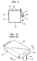
- Fig. 10 is a perspective view of the converter
- Fig. 11 is a sectional view thereof taken along the line XI-XI of Fig. 10.
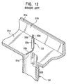
- Fig. 12 is a partially enlarged view of the converter, showing how a probe is installed.
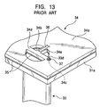
- Fig. 13 is a partially enlarged view of the converter, showing a circuit board mounted therein.
- a housing 31 and a waveguide 32 are manufactured by die-casting with a metal such as aluminum or zinc and then forming the components into one unit.
- the housing 31 is formed into a substantially rectangular box, including a bottom wall 31a, side walls 31b that are vertical and which surround the bottom wall 31a, a housing portion 31c that is uncovered and is defined by the side walls 31b, a penetrating hole 31d formed in the bottom wall 31a in the vicinity of one end thereof and extending perpendicularly thereto, and a stepped portion 31e having a step along an upper periphery of the side walls 31b.
- the waveguide 32 is a relatively narrow cylinder, extending from the bottom wall 31a at a position corresponding to the penetrating hole 31d.
- the waveguide 32 includes a substantially cylindrical tube section 32b having an opening 32a from which polarized waves are guided, a hollow 32c formed lengthwise at the center of the tube section 32b, and a holder portion 32d.
- the holder portion 32d is a semi-columnar recess, as shown in Fig. 12, which is formed in the tube section 32b to extend toward the opening 32a from a portion of the periphery of the penetrating hole 31d of the housing 31.
- a probe 33 for detecting horizontally polarized waves is composed of a tubular insulator 33a made of resin such as fluorine resin, polyethylene, or Teflon, and a linear core conductor 33b passing through the insulator 33a at the center thereof and mainly made of a metal such as brass or nickel.
- the core conductor 33b is formed into substantially an L-shape, leading to a first end 33c while the other end thereof, namely a second end 33d, is formed at the tip of the straight part.
- the insulator 33a is forced into the holder portion 32d in the waveguide 32, allowing the probe 33 to be installed into the waveguide 32. Once the probe 33 has been installed, the second end 33d of the core conductor 33b protrudes into the housing portion 31c of the housing 31 while the first end 33c extends into the hollow 32c of the waveguide 32.
- a rectangular circuit board 34 formed of a single insulating sheet.
- the circuit board 34 includes a thin flat plate 34a, three penetrating holes 34b formed in the vicinity of a side edge of the plate 34a and extending perpendicularly thereto, bridges 34d and 34e defining the penetrating holes 34b to form a T-shape, and a small opening 34c formed in the vicinity of the penetrating holes 34b.
- a copper ground conductor 35 is formed on the underside of the circuit board 34 except for the underside of the bridge 34e, and the underside of the bridge 34d serves as a short-circuit for the probe 33.
- a probe 36 for detecting vertically polarized waves is formed across the bridge 34e with a conductive pattern, and extends from the intersection of the bridges 34d and 34e toward the plate 34a of the circuit board 34.
- the probe 36 is connected to a circuit pattern (not shown) formed on the top of the plate 34a.
- the circuit board 34 is contained on the bottom wall 31a of the housing 31 so that the penetrating hole 31d may communicate with the penetrating holes 34b in the plate 34a.
- the second end 33d of the core conductor 33b of the probe 33 is inserted in the opening 34c in the plate 34a, and the circuit board 34 is then fixed to the bottom wall 31a of the housing 31 by any appropriate means.
- the second end 33d of the core conductor 33b that protrudes from the circuit board 34 is soldered by a solder 37 to the circuit pattern.
- a box-shaped metallic short-circuit wall 38 is formed by aluminum or zinc die-casting.
- the short-circuit wall 38 is mounted to the circuit board 34 by an appropriate technique such as caulking so as to cover the penetrating holes 34b in the circuit board 34.
- the short-circuit wall 38 has a base 38a acting as a short-circuit for the probe 36.
- a cover 39 formed of a single rectangular metal sheet is placed on the step 31e of the side walls 31b of the housing 31, and is fixed thereto by an appropriate technique. Accordingly, the housing portion 31c of the housing 31 is closed and electrically shielded.
- Such a conventional satellite broadcast receiving converter is of the type in which the housing 31 and the waveguide 32 are manufactured by die-casting such as aluminum die-casting and then forming the components into one unit. Therefore, a large number of materials are required, resulting in increased material costs as well as prolonged manufacturing time. This makes the converter expensive and less efficient in production.
- the housing 31 and the waveguide 32 have different sizes and configurations, and therefore more complex and expensive die-casting molds are required. This also makes the converter more expensive.
- a converter for satellite broadcast reception comprising: a box-shaped metallic housing; a cylindrical waveguide; and a probe attached to said waveguide, said probe having a cylindrical insulating portion and a central conductor piercing through a central part of said insulating portion, said waveguide being formed by bending a metallic plate and being integrally provided with a holding portion positioned outside the waveguide to hold said insulating portion of said probe.
- said insulating portion of said probe is held grippingly by both an outer surface of said waveguides and said holding portion.
- said holding portion is provided with a retaining piece for locking a free end side of the holding portion to said waveguide.
- said holding portion covers said probe throughout the whole in the longitudinal direction of said insulating portion which is exposed from said waveguide.
- said holding portion covers said probe throughout the whole in the longitudinal direction of said central conductor which is exposed from said waveguide.
- a satellite broadcast receiving converter that has a metal housing formed into a box, a tubular waveguide, and a box-shaped short-circuit wall which opposes the waveguide so as to communicate with a hollow formed in the waveguide, wherein the housing, the waveguide, and the short-circuit wall are joined together on a single metal sheet. These components are stamped out of the metal sheet, and then folded. With this feature, the number of materials making up the converter can be reduced. A simple manufacturing process as well as shortened manufacturing time can also be obtained.
- the converter may include a circuit board on which an electric circuit is formed, wherein the circuit board is held by and between the housing and an end of the waveguide. This enables the circuit board to be held therebetween in a simple manner.
- the waveguide includes a hooking tab at a free-end edge of the end thereof, which is engaged with the circuit board.
- a hooking ensures that the waveguide is mounted and positioned to the circuit board in a simple manner.
- a folding guide line is formed in a joining portion joining the housing with the waveguide, and the folding guide line may include cuts.
- the folding guide line facilitates folding of the waveguide at a predetermined position, so that the circuit board can be easily mounted to the waveguide.
- the present invention provides for a satellite broadcast receiving converter with a simple configuration having high production efficiency as well as high reliability. There is no need for an expensive die-casting mold, so that an inexpensive satellite broadcast receiving converter can be obtained.
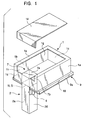
- Fig. 1 is an exploded perspective view of a satellite broadcast receiving converter in accordance with the present invention
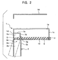
- Fig. 2 is an exploded sectional view of the converter.
- Fig. 3 is an illustration of the converter, showing that a waveguide and a circuit board are connected to each other.
- Fig. 4 is a developed view of a semi-finished product member, for illustrating the assembly of the converter.
- Fig. 5 is an enlarged view of the circuit board in the converter.
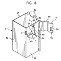
- Figs. 6 and 7 both illustrate that 4 probe is installed into the converter.
- Fig. 8 is a perspective view showing a modification of a holder portion in the converter.
- Fig. 9 is a top plan view showing another modification of a holder portion in the converter.
- a housing 1, a waveguide 2 and a short-circuit wall 7 are joined together on a single thin metal sheet. These components are stamped out of the metal sheet and folded.
- the housing 1 is formed into a box and is made of a thin metal sheet.
- the housing 1 has a rectangular recess 1g formed at the center thereof and a rectangular U-shaped top wall 1e that forms an edge of the periphery thereof.
- folded down side walls 1a, 1b, 1C and 1d are provided so as to be upright.
- Each of the side walls 1a, 1b. 1C and 1d is joined with the top wall 1e.
- An upper portion of the side wall 1d that opposes the side wall 1C is formed with a large cut-out indented portion 1h which extends across the width of the recess 1g.
- a plurality of substantially V-shaped hooking tabs 1f are formed at an edge of each of the side walls 1a, 1b and 1c
- the waveguide 2 is made of a thin metal sheet of a rectangular tube, including side panels 2a, 2b, 2c, and 2d, and a hollow 2e.
- the side panel 2a extends down from a joining portion 1i and the side wall 1d of the housing 1.
- the side panels 2b and 2d are angled at 90° relative to the side panel 2a.
- the side panel 2c is angled at 90° relative to the side panel 2b, and is joined with the side panel 2d so as to face the side panel 2a.
- the hollow 2e is defined by the side panels 2a, 2b, 2c and 2d.
- the side panels 2b, 2c and 2d provide ends 2f (see Fig. 6) that lie on free-end edges opposite to the joining portion 11. As shown in Figs.
- a substantially rectangular engagement hole 3 is formed in the boundary between the side panels 2a and 2d, and an insertion hole 4 composed of a round hole portion 4a and a square hole portion 4b is formed in the side panel 2d in the vicinity of the engagement hole 3.
- the joining portion 1i for joining the side panel 2a with the side wall 1d of the housing 1 includes a folding guide line 5 having cuts.
- the waveguide 2 extends perpendicularly to the housing 1 when it is folded and assembled, as shown in Fig. 1.
- the waveguide 2 can be tilted on the folding guide line 5 relative to the housing 1, as indicated by the dotted lines in Fig. 2.
- a holder portion 6 adjoins the side panel 2c by a joining portion 2h so as to be outside the waveguide 2.
- the holder portion 6 includes a body 6a of a flat sheet, a curved enclosing section 6b formed at the center of the body 6a, and a substantially V-shaped hooking tab 6c folded at an end of the holder portion 6, which lies on a free-end edge.
- the holder portion 6 can be folded down relative to the side panel 2c so that the hooking tab 6c can be engaged with the engagement hole 3 when the holder portion 6 is folded down to the side panel 2d.
- a short-circuit wall 7 is made of a thin metal sheet of a box-shape, including a lid 7a, side portions 7b, 7c, and 7d, and a cavity 7e.
- the lid 7a adjoins the side wall 1d of the housing 1, and is folded 90° relative to the side wall 1d.
- the side portions 7b, 7c, and 7d are folded down relative to the lid 7a.
- the cavity 7e is defined by the lid 7a, the side portions 7b, 7c, and 7d, and the side wall 1d.
- the short-circuit wall 7 is located in the housing 1 with the cavity 7e communicating with the hollow 2e of the waveguide 2.
- a probe 8 for detecting horizontally polarized waves including an L-shaped tubular insulator 8a made of resin such as fluorine resin, polyethylene, or Teflon, and a linear core conductor 8b passing through the center of the insulator 8a and mainly made of a metal such as brass or nickel.
- the core conductor 8b is bent substantially at a right angle together with the insulator 8a, leading to a first end 8c while the other end thereof, namely a second end 8d, is positioned substantially at a right angle relative to the first end 8c.
- the arrangement of the probe 8 is such that one end of the L-shaped insulator 8a is fitted into the round hole 4a of the insertion hole 4 formed in the side panel 2d of the waveguide 2 while the other end of the insulator 8a appearing from the waveguide 2 is held between an outer surface of the side panel 2d of the waveguide 2 and the enclosing section 6b of the holder portion 6.
- the enclosing section 6b of the holder portion 6 encloses the portion of the insulator 8a which appears from the waveguide 2 to hold the insulator 8a so that the portion of the core conductor 8b which appears from the waveguide 2 can be enclosed by the enclosing section 6b.
- the second end 8d of the core conductor 8b projects into the housing 1 while the first end 8c extends into the hollow 2e of the waveguide 2.
- a rectangular circuit board 9 made of a single insulating sheet, including a thin flat plate 9a, an indented portion 9b formed at one side of the plate 9a, three substantially rectangular penetrating holes 9c formed in the vicinity of the indented portion 9b and extending perpendicularly thereto, bridges 9g and 9h defining the penetrating holes 9c to form a T-shape, a small opening 9d formed in the vicinity of the penetrating holes 9c, two first engagement holes 9e formed in the vicinity of the penetrating holes 9c at the position opposite to the indented portion 9b, and a plurality of second engagement holes 9f formed at the peripheral edge of the circuit board 9.
- a copper ground conductor 10 is formed on the underside of the plate 9a except for the underside of the bridge 9h.
- a probe 11 for detecting vertically polarized waves is formed across the bridge 9h with a conductive pattern so as to extend from the intersection of the bridges 9g and 9h toward the plate 9a of the circuit board 9.
- the probe 11 is connected to a wiring pattern (not shown) formed on the top of the plate 9a.
- a strip-type copper ground pattern 12 encloses the penetrating holes 9c in the flat plate 9a so as to be connected with the ground conductor 10 via a plurality of through-holes 12a formed in the circuit board 9.
- the top surface of the flat plate 9a is brought into contact with the bottom ends of the side walls 1a, 1b, 1c, and 1d of the housing 1 while the undersurface of the flat plate 9a is brought into contact with and supported by the ends 2f of the waveguide 2.
- the hooking tabs 2g of the waveguide 2 are engaged with the first engagement holes 9e, and the hooking tabs 1f of the housing 1 are engaged with the second engagement holes 9f, whereby the circuit board 9 can be held between the housing 1 and the waveguide 2.
- the top surface of the flat plate 9a of the circuit board 9 is brought into contact with the bottom ends of the side portions 7b, 7c, and 7d of the short-circuit wall 7, and the side panel 2a of the waveguide 2 is engaged with the indented portion 9b of the flat plate 9a.
- the penetrating holes 9c in the circuit board 9 communicates with both the hollow 2e of the waveguide 2 and the cavity 7e of the short-circuit wall 7, and the side portions 7b, 7c, and 7d of the short-circuit wall 7 are in contact with the ground pattern 12.
- the second end 8d of the core conductor 8b of the probe 8 is inserted through the opening 9d in the flat plate 9a.
- the second end 8d of the core conductor 8b that projects from the circuit board 9 is soldered by a solder 13, and is connected to a wiring pattern formed on the circuit board 9.
- the penetrating holes 9c in the circuit board 9 are located within the waveguide 2 as well as within the short-circuit wall 7, and the underside of the circuit board 9 except for the underside of the bridge 9h is shielded with the ground conductor 10.
- An L-shaped cover 14 which is formed of a single rectangular metal sheet, is seated so as to match the side wall 1d and the top wall 1e of the housing 1, and is then fixed by an appropriate technique. This allows the housing 1 to be closed and electrically shielded.
- Fig. 4 illustrates a semi-finished product member 15 composed of the housing 1, the waveguide 2 and the short-circuit wall 7.
- the top wall 1e includes the recess 1g and the indented portion 1h at the center thereof, and the side walls 1a, 1b, 1c, and 1d extend from the four sides of the top wall 1e.
- the side panel 2a is continuous with the side wall 1d.
- the side panels 2b and 2c continuously extend from one side of the side panel 2a, and the side panel 2d is continuous with the other side of the side panel 2a.
- the holder portion 6 is further continuous with the side panel 2c via the joining portion 2h.
- the lid 7a is opposite to the side panel 2a via the side wall 1d, and the side portions 7b, 7c, and 7d extend outward from the lid 7a.
- the housing 1, the waveguide 2 and the short-circuit wall 7 are stamped out of a thin metal sheet to develop the semi-finished product member 15.
- the side walls 1a, 1b, 1c and 1d are folded by 90° at dotted lines A, to form the housing 1.
- the side panels 2b, 2c, and 2d are folded by 90° at dotted lines B and the side panels 2c and 2d are then connected to each other, forming the waveguide 2.
- the lid 7a is folded by 90° at a dotted line C and the side portions 7b, 7c, and 7d are folded by 90° at dotted lines D, forming the short-circuit wall 7.
- the configuration illustrated in Fig. 1 is thus obtained.
- the waveguide 2 extending perpendicularly to the housing 1 is tilted on a folding guide line 5 outward relative to the housing 1 as indicated by the dotted lines of Fig. 2 before positioning the circuit board 9. Then, the waveguide 2 is returned to the expected position to engage with the circuit board 9.
- the hooking tabs 1f of the housing 1 are engaged with the second engagement holes 9f in the circuit board 9 and the circuit board 9 is disposed beneath the housing 1.
- the hooking tabs 2g on the end 2f which lies on a free-end edge opposing to the side panel 2a continuous with the joining portion 1i, are engaged with the first engagement holes 9e in the circuit board 9 as shown in Fig. 3. This ensures that the circuit board 9 is held between the housing 1 and the waveguide 2.
- the installation of the probe 8 into the insertion hole 4 will now be described with reference to Fig. 6.
- the probe 8 is turned in the direction indicated by the arrow of Fig. 6 to guide the first end 8c of the core conductor 8b into the hollow 2e, followed by catching the insulator 8a against the round hole 4a, as shown in Fig. 7.
- the holder portion 6 is folded down at the joining portion 2h, and the hooking tab 6c on the end of the holder portion 6, which lies on a free-end edge, is engaged with the engagement hole 3 so that the insulator 8a is held between the enclosing section 6b and the side panel 2d to hold the probe 8.
- the satellite broadcast receiving converter has been described in conjunction with the arrangement and assembly thereof.
- two types of polarized waves orthogonal to each other are guided from the waveguide 2 into the hollow 2e.
- the horizontally polarized waves are reflected by a portion of the ground conductor 10 which is laid over the underside of the bridge 9g, and are then detected by the first end 8c of the probe 8 extending into the hollow 2e.
- the vertically polarized waves are reflected off of the lid 7a of the short-circuit wall 7, and are then detected by the probe 11 formed over the bridge 9h.
- the horizontally polarized waves detected by the probe 8 are transmitted as horizontally polarized signals to an electric circuit contained on the circuit board 9 via the core conductor 8b.
- the vertically polarized waves detected by the probe 11 are transmitted as vertically polarized signals to the electric circuit on the circuit board 9.
- the horizontally and vertically polarized signals transmitted from the probes 8 and 11, respectively, are combined on the circuit board 9.
- Figs. 8 and 9 modifications of the holder portion 6 are illustrated in Figs. 8 and 9.
- the holder portion 6 may not have a hooking tab, as shown in Fig. 8, and may hold the insulator 8a in such a manner that the holder portion 6 is left folded down at the joining portion 2h.
- the holder portion 6 shown in Fig. 9 encloses substantially the entire circumference of the insulator 8a and holds it.
- folding guide line 5 is not to be limited to one having cuts, as in the foregoing embodiment, but may be one having perforations or the like.
Landscapes
- Engineering & Computer Science (AREA)
- Manufacturing & Machinery (AREA)
- Waveguide Aerials (AREA)
- Structure Of Receivers (AREA)
- Waveguides (AREA)
- Casings For Electric Apparatus (AREA)
Abstract
Description
Claims (5)
- A converter for satellite broadcast reception, comprising:a box-shaped metallic housing;a cylindrical waveguide; anda probe attached to said waveguide, said probe having a cylindrical insulating portion and a central conductor piercing through a central part of said insulating portion,said waveguide being formed by bending a metallic plate and being integrally provided with a holding portion positioned outside the waveguide to hold said insulating portion of said probe.
- A converter for satellite broadcast reception according to Claim 1, wherein said insulating portion of said probe is held grippingly by both an outer surface of said waveguide and said holding portion.
- A converter for satellite broadcast reception according to Claim 1 or 2, wherein said holding portion is provided with a retaining piece for locking a free end side of the holding portion to said waveguide.
- A converter for satellite broadcast reception according to Claim 1, 2 or 3, wherein said holding portion covers said probe throughout the whole in the longitudinal direction of said insulating portion which is exposed from said waveguide.
- A converter for satellite broadcast reception according to Claim 1, 2 or 3, wherein said holding portion covers said probe throughout the whole in the longitudinal direction of said central conductor which is exposed from said waveguide.
Applications Claiming Priority (3)
| Application Number | Priority Date | Filing Date | Title |
|---|---|---|---|
| JP28353499A JP3771094B2 (en) | 1999-10-04 | 1999-10-04 | Converter for satellite broadcasting reception |
| JP28353499 | 1999-10-04 | ||
| EP00307744A EP1091443B1 (en) | 1999-10-04 | 2000-09-07 | Satellite broadcast receiving converter |
Related Parent Applications (1)
| Application Number | Title | Priority Date | Filing Date |
|---|---|---|---|
| EP00307744A Division EP1091443B1 (en) | 1999-10-04 | 2000-09-07 | Satellite broadcast receiving converter |
Publications (2)
| Publication Number | Publication Date |
|---|---|
| EP1349231A2 true EP1349231A2 (en) | 2003-10-01 |
| EP1349231A3 EP1349231A3 (en) | 2003-12-17 |
Family
ID=17666787
Family Applications (2)
| Application Number | Title | Priority Date | Filing Date |
|---|---|---|---|
| EP03015279A Withdrawn EP1349231A3 (en) | 1999-10-04 | 2000-09-07 | Satellite broadcast receiving converter |
| EP00307744A Expired - Lifetime EP1091443B1 (en) | 1999-10-04 | 2000-09-07 | Satellite broadcast receiving converter |
Family Applications After (1)
| Application Number | Title | Priority Date | Filing Date |
|---|---|---|---|
| EP00307744A Expired - Lifetime EP1091443B1 (en) | 1999-10-04 | 2000-09-07 | Satellite broadcast receiving converter |
Country Status (7)
| Country | Link |
|---|---|
| US (1) | US6658233B1 (en) |
| EP (2) | EP1349231A3 (en) |
| JP (1) | JP3771094B2 (en) |
| CN (1) | CN1193515C (en) |
| DE (1) | DE60011201T2 (en) |
| MX (1) | MXPA00009714A (en) |
| TW (1) | TW497375B (en) |
Cited By (1)
| Publication number | Priority date | Publication date | Assignee | Title |
|---|---|---|---|---|
| US7228101B2 (en) * | 2002-12-17 | 2007-06-05 | Sharp Kabushiki Kaisha | Satellite broadcast reception converter |
Families Citing this family (13)
| Publication number | Priority date | Publication date | Assignee | Title |
|---|---|---|---|---|
| EP1168486A1 (en) | 2000-04-20 | 2002-01-02 | Alps Electric Co., Ltd. | Converter for satellite broadcast reception |
| JP3916530B2 (en) * | 2002-08-05 | 2007-05-16 | アルプス電気株式会社 | Converter for satellite broadcasting reception |
| JP4027175B2 (en) * | 2002-08-05 | 2007-12-26 | アルプス電気株式会社 | Converter for satellite broadcasting reception |
| JP4742332B1 (en) * | 2010-12-15 | 2011-08-10 | ナルックス株式会社 | Molded part for casing and its mold |
| US10468736B2 (en) | 2017-02-08 | 2019-11-05 | Aptiv Technologies Limited | Radar assembly with ultra wide band waveguide to substrate integrated waveguide transition |
| US11757166B2 (en) * | 2020-11-10 | 2023-09-12 | Aptiv Technologies Limited | Surface-mount waveguide for vertical transitions of a printed circuit board |
| US11616306B2 (en) | 2021-03-22 | 2023-03-28 | Aptiv Technologies Limited | Apparatus, method and system comprising an air waveguide antenna having a single layer material with air channels therein which is interfaced with a circuit board |
| CN113270703B (en) * | 2021-04-01 | 2022-01-11 | 武汉虹信科技发展有限责任公司 | Dual-polarization multi-input multi-output metal plate combiner and base station antenna |
| EP4084222A1 (en) | 2021-04-30 | 2022-11-02 | Aptiv Technologies Limited | Dielectric loaded waveguide for low loss signal distributions and small form factor antennas |
| US12224502B2 (en) | 2021-10-14 | 2025-02-11 | Aptiv Technologies AG | Antenna-to-printed circuit board transition |
| US12265172B2 (en) | 2022-05-25 | 2025-04-01 | Aptiv Technologies AG | Vertical microstrip-to-waveguide transition |
| US12424767B2 (en) | 2022-11-15 | 2025-09-23 | Aptiv Technologies AG | Planar surface features for waveguide and antenna |
| US12506272B2 (en) | 2023-05-16 | 2025-12-23 | Aptiv Technologies AG | Production-tolerant multi-part antenna system |
Family Cites Families (15)
| Publication number | Priority date | Publication date | Assignee | Title |
|---|---|---|---|---|
| DE1616800B1 (en) * | 1964-07-24 | 1971-04-08 | Sony Corp | DEVICE FOR INSERTING A COAXIAL CABLE INTO A CAVITY RESONATOR FOR HIGH-FREQUENCY ELECTRICAL VIBRATIONS |
| US4058813A (en) * | 1976-03-18 | 1977-11-15 | Rca Corporation | Sheet metal waveguide horn antenna |
| JPS59132207A (en) * | 1983-01-19 | 1984-07-30 | Fujitsu Ltd | Manufacture of rectangular waveguide |
| US4679249A (en) * | 1984-02-15 | 1987-07-07 | Matsushita Electric Industrial Co., Ltd. | Waveguide-to-microstrip line coupling arrangement and a frequency converter having the coupling arrangement |
| GB2185920B (en) * | 1986-01-24 | 1989-11-01 | Quasar Microwave Tech | Manufacture of waveguides and like tubular elements |
| JPS63199508A (en) * | 1987-02-13 | 1988-08-18 | Sharp Corp | Amplifier circuit for low noise microwave |
| JPH0174613U (en) * | 1987-07-06 | 1989-05-19 | ||
| AT393054B (en) * | 1989-07-27 | 1991-08-12 | Siemens Ag Oesterreich | TRANSMITTER AND / OR RECEIVING ARRANGEMENT FOR PORTABLE DEVICES |
| US5225799A (en) * | 1991-06-04 | 1993-07-06 | California Amplifier | Microwave filter fabrication method and filters therefrom |
| JP3071136B2 (en) * | 1995-03-07 | 2000-07-31 | シャープ株式会社 | Terminal structure and universal LNB using this |
| GB2334153B (en) * | 1995-07-19 | 1999-11-17 | Alps Electric Co Ltd | Outdoor converter for receiving satellite broadcast |
| IT1284026B1 (en) * | 1996-06-18 | 1998-05-08 | Italtel Spa | SUBHARMONIC FREQUENCY CONVERTER FOR MILLIMETRIC RADIO WAVES APPLICATIONS |
| JPH1117573A (en) | 1997-06-18 | 1999-01-22 | Kyong In Electron Co Ltd | Low noise block converter for satellite broadcast |
| JPH1174809A (en) | 1997-08-27 | 1999-03-16 | Alps Electric Co Ltd | Satellite broadcast reception converter |
| US6127901A (en) * | 1999-05-27 | 2000-10-03 | Hrl Laboratories, Llc | Method and apparatus for coupling a microstrip transmission line to a waveguide transmission line for microwave or millimeter-wave frequency range transmission |
-
1999
- 1999-10-04 JP JP28353499A patent/JP3771094B2/en not_active Expired - Fee Related
-
2000
- 2000-09-07 DE DE60011201T patent/DE60011201T2/en not_active Expired - Fee Related
- 2000-09-07 EP EP03015279A patent/EP1349231A3/en not_active Withdrawn
- 2000-09-07 EP EP00307744A patent/EP1091443B1/en not_active Expired - Lifetime
- 2000-09-14 TW TW089118865A patent/TW497375B/en not_active IP Right Cessation
- 2000-09-29 CN CNB001295020A patent/CN1193515C/en not_active Expired - Fee Related
- 2000-10-03 MX MXPA00009714A patent/MXPA00009714A/en unknown
- 2000-10-03 US US09/677,809 patent/US6658233B1/en not_active Expired - Fee Related
Cited By (1)
| Publication number | Priority date | Publication date | Assignee | Title |
|---|---|---|---|---|
| US7228101B2 (en) * | 2002-12-17 | 2007-06-05 | Sharp Kabushiki Kaisha | Satellite broadcast reception converter |
Also Published As
| Publication number | Publication date |
|---|---|
| JP2001111256A (en) | 2001-04-20 |
| CN1193515C (en) | 2005-03-16 |
| EP1091443A2 (en) | 2001-04-11 |
| EP1091443B1 (en) | 2004-06-02 |
| DE60011201T2 (en) | 2005-07-07 |
| EP1091443A3 (en) | 2002-07-03 |
| CN1291009A (en) | 2001-04-11 |
| EP1349231A3 (en) | 2003-12-17 |
| DE60011201D1 (en) | 2004-07-08 |
| JP3771094B2 (en) | 2006-04-26 |
| TW497375B (en) | 2002-08-01 |
| US6658233B1 (en) | 2003-12-02 |
| MXPA00009714A (en) | 2002-12-16 |
Similar Documents
| Publication | Publication Date | Title |
|---|---|---|
| EP1091443B1 (en) | Satellite broadcast receiving converter | |
| CN100361352C (en) | Connector with a locking member | |
| US6439901B1 (en) | Electrical connector with releasable pick-up device | |
| WO2000016449A1 (en) | Connector socket, connector plug and connector assembly | |
| US5759050A (en) | Electrical connection construction between electrical connection box and electronic circuit unit | |
| JP2004259672A (en) | Coaxial connector | |
| US5415563A (en) | Wire connecting apparatus and terminal therefor | |
| US7044782B2 (en) | Electrical connector | |
| JP3870769B2 (en) | Connector mounting structure | |
| EP1168486A1 (en) | Converter for satellite broadcast reception | |
| JP5054492B2 (en) | Multipole coaxial connector | |
| JP3268518B2 (en) | Electrical equipment | |
| JPH05182700A (en) | Terminal device | |
| JPH077184U (en) | Circuit board housing structure | |
| JPH08227736A (en) | Connecting structure of electric connection box | |
| JP2001177302A (en) | Converter for receiving satellite broadcast | |
| JP3565817B2 (en) | Coaxial cable connector | |
| JPH083026Y2 (en) | Code introduction mechanism for circuit board in case | |
| KR100351770B1 (en) | Connector attachable slide-type electronic component | |
| JP3565816B2 (en) | Plug connector | |
| JPH0737267Y2 (en) | Coaxial connector between chassis and its case | |
| JP2004119253A (en) | Terminal fitting | |
| JP3916530B2 (en) | Converter for satellite broadcasting reception | |
| JPH0353431Y2 (en) | ||
| JP2003046324A (en) | Antenna |
Legal Events
| Date | Code | Title | Description |
|---|---|---|---|
| PUAI | Public reference made under article 153(3) epc to a published international application that has entered the european phase |
Free format text: ORIGINAL CODE: 0009012 |
|
| 17P | Request for examination filed |
Effective date: 20030707 |
|
| AC | Divisional application: reference to earlier application |
Ref document number: 1091443 Country of ref document: EP Kind code of ref document: P |
|
| AK | Designated contracting states |
Kind code of ref document: A2 Designated state(s): DE FR GB |
|
| PUAL | Search report despatched |
Free format text: ORIGINAL CODE: 0009013 |
|
| AK | Designated contracting states |
Kind code of ref document: A3 Designated state(s): DE FR GB |
|
| 17Q | First examination report despatched |
Effective date: 20040715 |
|
| AKX | Designation fees paid |
Designated state(s): DE FR GB |
|
| STAA | Information on the status of an ep patent application or granted ep patent |
Free format text: STATUS: THE APPLICATION IS DEEMED TO BE WITHDRAWN |
|
| 18D | Application deemed to be withdrawn |
Effective date: 20041126 |