EP1348992B1 - Optical waveguide device - Google Patents
Optical waveguide device Download PDFInfo
- Publication number
- EP1348992B1 EP1348992B1 EP01273335A EP01273335A EP1348992B1 EP 1348992 B1 EP1348992 B1 EP 1348992B1 EP 01273335 A EP01273335 A EP 01273335A EP 01273335 A EP01273335 A EP 01273335A EP 1348992 B1 EP1348992 B1 EP 1348992B1
- Authority
- EP
- European Patent Office
- Prior art keywords
- film
- optical
- optical waveguide
- substrate
- waveguide device
- Prior art date
- Legal status (The legal status is an assumption and is not a legal conclusion. Google has not performed a legal analysis and makes no representation as to the accuracy of the status listed.)
- Expired - Lifetime
Links
- 230000003287 optical effect Effects 0.000 title claims description 107
- 239000000758 substrate Substances 0.000 claims description 32
- 238000004544 sputter deposition Methods 0.000 claims description 13
- 238000007740 vapor deposition Methods 0.000 claims description 13
- VYPSYNLAJGMNEJ-UHFFFAOYSA-N Silicium dioxide Chemical compound O=[Si]=O VYPSYNLAJGMNEJ-UHFFFAOYSA-N 0.000 claims description 11
- 229910052814 silicon oxide Inorganic materials 0.000 claims description 11
- 230000000694 effects Effects 0.000 claims description 5
- 230000001902 propagating effect Effects 0.000 claims 1
- 239000012071 phase Substances 0.000 description 19
- 238000004891 communication Methods 0.000 description 9
- 239000013307 optical fiber Substances 0.000 description 9
- 238000000034 method Methods 0.000 description 8
- 239000000463 material Substances 0.000 description 5
- GQYHUHYESMUTHG-UHFFFAOYSA-N lithium niobate Chemical compound [Li+].[O-][Nb](=O)=O GQYHUHYESMUTHG-UHFFFAOYSA-N 0.000 description 4
- 230000005540 biological transmission Effects 0.000 description 3
- 150000002500 ions Chemical class 0.000 description 3
- 230000007774 longterm Effects 0.000 description 3
- 230000000704 physical effect Effects 0.000 description 3
- WSMQKESQZFQMFW-UHFFFAOYSA-N 5-methyl-pyrazole-3-carboxylic acid Chemical compound CC1=CC(C(O)=O)=NN1 WSMQKESQZFQMFW-UHFFFAOYSA-N 0.000 description 2
- XKRFYHLGVUSROY-UHFFFAOYSA-N Argon Chemical compound [Ar] XKRFYHLGVUSROY-UHFFFAOYSA-N 0.000 description 2
- 230000015572 biosynthetic process Effects 0.000 description 2
- 229910052802 copper Inorganic materials 0.000 description 2
- 239000010949 copper Substances 0.000 description 2
- 239000013078 crystal Substances 0.000 description 2
- 238000003780 insertion Methods 0.000 description 2
- 230000037431 insertion Effects 0.000 description 2
- 239000002245 particle Substances 0.000 description 2
- 239000008188 pellet Substances 0.000 description 2
- RYGMFSIKBFXOCR-UHFFFAOYSA-N Copper Chemical compound [Cu] RYGMFSIKBFXOCR-UHFFFAOYSA-N 0.000 description 1
- MYMOFIZGZYHOMD-UHFFFAOYSA-N Dioxygen Chemical compound O=O MYMOFIZGZYHOMD-UHFFFAOYSA-N 0.000 description 1
- 229910052581 Si3N4 Inorganic materials 0.000 description 1
- RTAQQCXQSZGOHL-UHFFFAOYSA-N Titanium Chemical compound [Ti] RTAQQCXQSZGOHL-UHFFFAOYSA-N 0.000 description 1
- 229910052786 argon Inorganic materials 0.000 description 1
- QVGXLLKOCUKJST-UHFFFAOYSA-N atomic oxygen Chemical compound [O] QVGXLLKOCUKJST-UHFFFAOYSA-N 0.000 description 1
- 230000003247 decreasing effect Effects 0.000 description 1
- 238000000151 deposition Methods 0.000 description 1
- 238000009792 diffusion process Methods 0.000 description 1
- 229910001882 dioxygen Inorganic materials 0.000 description 1
- 239000006185 dispersion Substances 0.000 description 1
- 238000010894 electron beam technology Methods 0.000 description 1
- 239000000835 fiber Substances 0.000 description 1
- 239000007789 gas Substances 0.000 description 1
- 229910052737 gold Inorganic materials 0.000 description 1
- 230000010354 integration Effects 0.000 description 1
- 238000005468 ion implantation Methods 0.000 description 1
- 229910052746 lanthanum Inorganic materials 0.000 description 1
- FZLIPJUXYLNCLC-UHFFFAOYSA-N lanthanum atom Chemical compound [La] FZLIPJUXYLNCLC-UHFFFAOYSA-N 0.000 description 1
- 238000004519 manufacturing process Methods 0.000 description 1
- 238000012986 modification Methods 0.000 description 1
- 230000004048 modification Effects 0.000 description 1
- TWNQGVIAIRXVLR-UHFFFAOYSA-N oxo(oxoalumanyloxy)alumane Chemical compound O=[Al]O[Al]=O TWNQGVIAIRXVLR-UHFFFAOYSA-N 0.000 description 1
- 239000001301 oxygen Substances 0.000 description 1
- 229910052760 oxygen Inorganic materials 0.000 description 1
- 238000007747 plating Methods 0.000 description 1
- 230000010287 polarization Effects 0.000 description 1
- 230000000754 repressing effect Effects 0.000 description 1
- 238000012827 research and development Methods 0.000 description 1
- HQVNEWCFYHHQES-UHFFFAOYSA-N silicon nitride Chemical compound N12[Si]34N5[Si]62N3[Si]51N64 HQVNEWCFYHHQES-UHFFFAOYSA-N 0.000 description 1
- 229910052709 silver Inorganic materials 0.000 description 1
- 238000001947 vapour-phase growth Methods 0.000 description 1
Images

Classifications
-
- G—PHYSICS
- G02—OPTICS
- G02F—OPTICAL DEVICES OR ARRANGEMENTS FOR THE CONTROL OF LIGHT BY MODIFICATION OF THE OPTICAL PROPERTIES OF THE MEDIA OF THE ELEMENTS INVOLVED THEREIN; NON-LINEAR OPTICS; FREQUENCY-CHANGING OF LIGHT; OPTICAL LOGIC ELEMENTS; OPTICAL ANALOGUE/DIGITAL CONVERTERS
- G02F1/00—Devices or arrangements for the control of the intensity, colour, phase, polarisation or direction of light arriving from an independent light source, e.g. switching, gating or modulating; Non-linear optics
- G02F1/01—Devices or arrangements for the control of the intensity, colour, phase, polarisation or direction of light arriving from an independent light source, e.g. switching, gating or modulating; Non-linear optics for the control of the intensity, phase, polarisation or colour
- G02F1/03—Devices or arrangements for the control of the intensity, colour, phase, polarisation or direction of light arriving from an independent light source, e.g. switching, gating or modulating; Non-linear optics for the control of the intensity, phase, polarisation or colour based on ceramics or electro-optical crystals, e.g. exhibiting Pockels effect or Kerr effect
- G02F1/0305—Constructional arrangements
- G02F1/0322—Arrangements comprising two or more independently controlled crystals
-
- G—PHYSICS
- G02—OPTICS
- G02F—OPTICAL DEVICES OR ARRANGEMENTS FOR THE CONTROL OF LIGHT BY MODIFICATION OF THE OPTICAL PROPERTIES OF THE MEDIA OF THE ELEMENTS INVOLVED THEREIN; NON-LINEAR OPTICS; FREQUENCY-CHANGING OF LIGHT; OPTICAL LOGIC ELEMENTS; OPTICAL ANALOGUE/DIGITAL CONVERTERS
- G02F1/00—Devices or arrangements for the control of the intensity, colour, phase, polarisation or direction of light arriving from an independent light source, e.g. switching, gating or modulating; Non-linear optics
- G02F1/01—Devices or arrangements for the control of the intensity, colour, phase, polarisation or direction of light arriving from an independent light source, e.g. switching, gating or modulating; Non-linear optics for the control of the intensity, phase, polarisation or colour
- G02F1/03—Devices or arrangements for the control of the intensity, colour, phase, polarisation or direction of light arriving from an independent light source, e.g. switching, gating or modulating; Non-linear optics for the control of the intensity, phase, polarisation or colour based on ceramics or electro-optical crystals, e.g. exhibiting Pockels effect or Kerr effect
- G02F1/035—Devices or arrangements for the control of the intensity, colour, phase, polarisation or direction of light arriving from an independent light source, e.g. switching, gating or modulating; Non-linear optics for the control of the intensity, phase, polarisation or colour based on ceramics or electro-optical crystals, e.g. exhibiting Pockels effect or Kerr effect in an optical waveguide structure
-
- G—PHYSICS
- G02—OPTICS
- G02F—OPTICAL DEVICES OR ARRANGEMENTS FOR THE CONTROL OF LIGHT BY MODIFICATION OF THE OPTICAL PROPERTIES OF THE MEDIA OF THE ELEMENTS INVOLVED THEREIN; NON-LINEAR OPTICS; FREQUENCY-CHANGING OF LIGHT; OPTICAL LOGIC ELEMENTS; OPTICAL ANALOGUE/DIGITAL CONVERTERS
- G02F1/00—Devices or arrangements for the control of the intensity, colour, phase, polarisation or direction of light arriving from an independent light source, e.g. switching, gating or modulating; Non-linear optics
- G02F1/01—Devices or arrangements for the control of the intensity, colour, phase, polarisation or direction of light arriving from an independent light source, e.g. switching, gating or modulating; Non-linear optics for the control of the intensity, phase, polarisation or colour
- G02F1/03—Devices or arrangements for the control of the intensity, colour, phase, polarisation or direction of light arriving from an independent light source, e.g. switching, gating or modulating; Non-linear optics for the control of the intensity, phase, polarisation or colour based on ceramics or electro-optical crystals, e.g. exhibiting Pockels effect or Kerr effect
- G02F1/035—Devices or arrangements for the control of the intensity, colour, phase, polarisation or direction of light arriving from an independent light source, e.g. switching, gating or modulating; Non-linear optics for the control of the intensity, phase, polarisation or colour based on ceramics or electro-optical crystals, e.g. exhibiting Pockels effect or Kerr effect in an optical waveguide structure
- G02F1/0356—Devices or arrangements for the control of the intensity, colour, phase, polarisation or direction of light arriving from an independent light source, e.g. switching, gating or modulating; Non-linear optics for the control of the intensity, phase, polarisation or colour based on ceramics or electro-optical crystals, e.g. exhibiting Pockels effect or Kerr effect in an optical waveguide structure controlled by a high-frequency electromagnetic wave component in an electric waveguide structure
-
- G—PHYSICS
- G02—OPTICS
- G02F—OPTICAL DEVICES OR ARRANGEMENTS FOR THE CONTROL OF LIGHT BY MODIFICATION OF THE OPTICAL PROPERTIES OF THE MEDIA OF THE ELEMENTS INVOLVED THEREIN; NON-LINEAR OPTICS; FREQUENCY-CHANGING OF LIGHT; OPTICAL LOGIC ELEMENTS; OPTICAL ANALOGUE/DIGITAL CONVERTERS
- G02F2201/00—Constructional arrangements not provided for in groups G02F1/00 - G02F7/00
- G02F2201/07—Constructional arrangements not provided for in groups G02F1/00 - G02F7/00 buffer layer
-
- G—PHYSICS
- G02—OPTICS
- G02F—OPTICAL DEVICES OR ARRANGEMENTS FOR THE CONTROL OF LIGHT BY MODIFICATION OF THE OPTICAL PROPERTIES OF THE MEDIA OF THE ELEMENTS INVOLVED THEREIN; NON-LINEAR OPTICS; FREQUENCY-CHANGING OF LIGHT; OPTICAL LOGIC ELEMENTS; OPTICAL ANALOGUE/DIGITAL CONVERTERS
- G02F2201/00—Constructional arrangements not provided for in groups G02F1/00 - G02F7/00
- G02F2201/16—Constructional arrangements not provided for in groups G02F1/00 - G02F7/00 series; tandem
-
- G—PHYSICS
- G02—OPTICS
- G02F—OPTICAL DEVICES OR ARRANGEMENTS FOR THE CONTROL OF LIGHT BY MODIFICATION OF THE OPTICAL PROPERTIES OF THE MEDIA OF THE ELEMENTS INVOLVED THEREIN; NON-LINEAR OPTICS; FREQUENCY-CHANGING OF LIGHT; OPTICAL LOGIC ELEMENTS; OPTICAL ANALOGUE/DIGITAL CONVERTERS
- G02F2203/00—Function characteristic
- G02F2203/21—Thermal instability, i.e. DC drift, of an optical modulator; Arrangements or methods for the reduction thereof
-
- G—PHYSICS
- G02—OPTICS
- G02F—OPTICAL DEVICES OR ARRANGEMENTS FOR THE CONTROL OF LIGHT BY MODIFICATION OF THE OPTICAL PROPERTIES OF THE MEDIA OF THE ELEMENTS INVOLVED THEREIN; NON-LINEAR OPTICS; FREQUENCY-CHANGING OF LIGHT; OPTICAL LOGIC ELEMENTS; OPTICAL ANALOGUE/DIGITAL CONVERTERS
- G02F2203/00—Function characteristic
- G02F2203/50—Phase-only modulation
Definitions
- This invention relates to an optical waveguide device, on which plural elements with different functions are integrated, and particularly usable for long-haul and high-capacity optical fiber communication systems and optical measuring instruments.
- JP7-280088 discloses a waveguide electro-optical element wherein a DC-drift phenomenon is reduced.
- a low density first buffer layer is formed by vapor phase deposition without using a high-energy ion species, for example, vacuum vapor deposition, and thereafter, a high-density second buffer layer is formed by a vapor-phased deposition method wherein a high-energy ion species is used, for example, an ion-assisted vacuum vapor deposition method or a sputtering method.
- An optical waveguide device comprising of an optical waveguide, a buffer layer and traveling-wave type electrodes which are integrated on a substrate having an electro-optic effect made of lithium niobate (LN) or the like, has been widely employed for long-haul and high-capacity optical fiber communication systems and optical measuring instruments.
- an optical intensity modulator, an optical phase modulator and a polarization scrambler are frequently employed as a key device for optical fiber communication systems.
- the optical fiber communication system is required to have faster transmission speed and higher capacity. Then, in order to realize such a highspeed and high-capacity optical fiber communication system, it is required to repress the broadening of an optical pulse due to the slight optical dispersion in an optical fiber employed as a transmission line.
- the chirp degree in the optical fiber communication system is controlled by an optical phase modulator placed after an optical intensity modulator as a converter of an electric signal into an optical pulse and thus, improve the transmission performance of the system.
- Such a monolithically integrated optical device is fabricated as follows. First of all, optical waveguides are formed on a given substrate according to the required function, such as optical intensity modulation and optical phase modulation. Then, a buffer layer is formed uniformly on the substrate, and electrodes are formed on the substrate via the buffer layer. As a result, an optical waveguide device on which an optical intensity modulator and an optical phase modulator are monolithically integrated is completed.
- the optical intensity modulator and the optical phase modulator are fabricated on the same condition except their optical waveguide pattern.
- the optical waveguide device can not achieve the designed characteristics.
- a DC voltage is applied to the optical intensity modulator so as to control the operation point
- a relatively large DC drift may occur depending on the fabricating condition of the optical intensity modulator, so that the long-term reliability of the optical intensity modulator may be deteriorated.
- the plural modulators are fabricated on the same substrate to complete an integrated optical waveguide device, as mentioned above, the long-term reliability of the resultant optical waveguide device may be deteriorated.
- this invention relates to an optical waveguide device having the features defined in claim 1.
- the inventors had studied intensively to find the cause of the insufficient performance of each modulator in an integrated optical waveguide device on which an optical intensity modulator and an optical phase modulator are monolithically integrated.
- the physical property of the buffer layer significantly affects the performance of each modulator. Namely, in a conventional integrated optical device, the buffer layer is formed uniformly on the substrate, so that each modulator is fabricated on the same buffer layer. Therefore, the buffer layer is not formed so as to satisfy the physical properties to be required in each modulator.
- the buffer layer of the optical intensity modulator has low density.
- the buffer layer constituting the optical phase modulator preferably has high density because a DC voltage is not necessary to apply and attenuation of microwave traveling in the electrodes is reduced.
- monolithically integrated optical intensity modulator and the optical phase modulator can exhibit their inherent performances since the buffer layer is composed of a first film and a second film which have preferable physical properties for each modulator, as mentioned in the above example. Therefore, the integrated optical waveguide device can achieve the designed characteristics.
- the ratio (n1/n2) of the refractive index n1 of the first film at a wavelength of 633nm to the refractive index n2 of the second film at a wavelength of 633nm is set to be 1.010 or over.
- the refractive index of a film strongly depends on the film density when the film is made of the same material. Therefore, the refractive index of the film is increased as the film density is increased.
- the above-mentioned requirement means that the density of the first film is higher than that of the second film by a given value.
- each modulator can exhibit its inherent performance. Therefore, the integrated optical waveguide device can achieve the designed characteristics effectively and efficiently .
- the refractive index n1 of the first film at a wavelength of 633nm is set to be 1.455 or over and the refractive index n2 of the second film at a wavelength of 633nm is set to be 1.440 or below.
- each modulator when the optical phase modulator is formed on the first film and the optical intensity modulator is formed on the second film, each modulator can exhibit its inherent performance sufficiently since the density of the first film can be set much higher than that of the second film, and thus, the optical waveguide device can achieve the designed characteristics more sufficiently.
- the first film and the second film are formed by means of sputtering or vapor deposition, preferably so as to satisfy the above-mentioned requirements for refractive indexes.
- the density of a film fabricated by sputtering is high, and the density of a film fabricated by vapor deposition is low. Therefore, according to the present invention, the first film is formed by sputtering and the second film is formed by vapor deposition.
- Fig. 1 is a perspective view showing an optical waveguide device according to the present invention.
- An optical waveguide device 10 illustrated in Fig. 1 includes a substrate 1 made of the material having an electro-optic effect, an optical waveguide 2 formed on the surface of the substrate 1, signal electrodes 3 and 4, and ground electrodes 5, 6 and 7.
- a first film 8 is formed between the substrate 1 and the electrodes 3, 5 and 6, and a second film 9 is formed between the substrate 1 and the electrodes 4, 6 and 7.
- An optical phase modulator 10A is composed of the substrate 1, the optical waveguide 2, the signal electrode 3, the ground electrodes 5 and 6, and the first film 8.
- a DC applied-type optical intensity modulator 10B is composed of the substrate 1, the optical waveguide 2, the signal electrode 4, the ground electrodes 6 and 7, and the second film 9. Therefore, the optical waveguide device 10 is composed of the optical phase modulator 10A and the optical intensity modulator 10B, which are monolithically integrated on the substrate 1.
- the first film 8 and the second film 9 are provided as buffer layers for the optical phase modulator 10A and the optical intensity modulator 10B, respectively.
- the ratio (n1/n2 of the refractive index n1 of the first film 8 constituting the optical phase modulator 10A at a wavelength of 633nm to the refractive index n2 of the second film 9 constituting the optical intensity modulator 10B at a wavelength of 633nm is set to be 1.010 or over, particularly 1.021 or over.
- the density of the first film 8 is relatively higher than that of the second film 9.
- the optical phase modulator 10A is composed of a buffer layer having a higher density, so that the attenuation of microwave applied to the signal electrode 3 can be repressed effectively.
- the optical intensity modulator 10B is composed of a buffer layer having a lower density, so that the DC drift can be reduced effectively when a DC voltage is applied to the signal electrode 4.
- the refractive index n1 of the first film 8 is set to be 1.455 or over, particularly 1.460 or over. In this case, the attenuation of microwave can be repressed more effectively.
- the refractive index n2 of the second film 9 is set to be 1.440 or below, particularly 1.430 or below. In this case, the DC drift occurring when the DC voltage is applied can be reduced more effectively.
- the high refractive index film that is, high-density first film 8 is formed by means of sputtering.
- the chamber of the sputtering apparatus is evacuated until the degree of vacuum reaches to 1.3 ⁇ 10 -5 Pa (10 -7 Torr) or below.
- an argon gas and an oxygen gas are introduced into the sputtering chamber until the interior pressure reaches about 0.13 Pa (10 -3 Torr).
- a given high frequency electric power is supplied to a silicon oxide target to deposit silicon oxide particles on a given substrate.
- the low refractive index film that is, low-density second film 9 is formed by means of vapor deposition.
- silicon oxide pellets are charged into a copper crucible or the like, and then, electron beams are irradiated onto the pellets so as to be vaporized. As a result, silicon oxide particles are deposited on a given substrate.
- the first film 8 and the second film 9 may be formed independently by means of sputtering and vapor deposition by attaching a given mask on the substrate 1.
- a given film is formed uniformly by means of sputtering or vapor deposition, and then, removed partially. Thereafter, another film is formed at the removed area by means of vapor deposition or sputtering to complete the first film 8 and the second film 9.
- the first film 8 and the second film 9 constituting the buffer layers for the optical phase modulator 10A and the optical intensity modulator 10B
- the first film 8 and the second film 9 may be annealed under an atmosphere that at least includes oxygen, so as to improve the mechanical properties of the films 8 and 9 and compensate oxygen-starved portions of the films 8 and 9.
- the substrate 1 may be made of a dielectric single crystal having an electro-optic effect such as lithium niobate (LN), lithium tantalate (LT), and lead lanthanum zirconate titanate (PLZT). Then, an X-cut face, a Y-cut face or a Z-cut face of such a single crystal may be employed as the main surface of the substrate 1.
- LN lithium niobate
- LT lithium tantalate
- PZT lead lanthanum zirconate titanate
- the optical waveguide 2 may be formed by means of Ti thermal diffusion method, proton exchange method, ion implantation method or epitaxial growth method.
- the signal electrodes 3 and 4 and the ground electrodes 5-7 may be made of Au, Ag or Cu by means of vapor deposition method, plating method or the combination thereof.
- the first film 8 and the second film 9 may be made of other material, i.e., aluminum oxide, silicon nitride or the combination thereof, instead of silicon oxide.
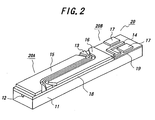
- Fig. 2 is a perspective view showing another optical waveguide device according to the present invention.
- An optical waveguide device 20 illustrated in Fig. 2 includes a substrate 11 made of the material having an electro-optic effect, an optical waveguide 12 formed on the surface of the substrate 11, signal electrodes 13 and 14, and ground electrodes 15, 16 and 17.
- a first film 18 is formed between the substrate 11 and the electrodes 13, 15 and 16, and a second film 19 is formed between the substrate 11 and the electrodes 14 and 17.
- An RF applied-type optical intensity modulator 20A is composed of the substrate 11, the optical waveguide 12, the signal electrode 13, the ground electrodes 15 and 16, and the first film 18.
- a DC electrode section 20B is composed of the substrate 11, the optical waveguide 12, the signal electrode 14, the ground electrode 17, and the second film 19. Therefore, the optical waveguide device 20 is composed of the optical intensity modulator 20A and the DC electrode section 20B, which are monolithically integrated on the substrate 11.
- the first film 18 and the second film 19 are provided as buffer layers for the optical intensity modulator 20A and the DC electrode section 20B, respectively.
- the ratio (n1/n2 of the refractive index n1 of the first film 18 constituting the optical intensity modulator 20A at a wavelength of 633nm to the refractive index n2 of the second film 19 constituting the DC electrode section 20B at a wavelength of 633nm is also set to be 1.010 or over, particularly 1.021 or over.
- the attenuation of microwave applied to the signal electrode 13 of the optical intensity modulator 20A can be repressed effectively, and the DC drift can be reduced effectively when a DC voltage is applied to the signal electrode 14 of the DC electrode section 20B.
- the refractive index n1 of the first film 18 is set to be 1.455 or over and the refractive index n2 of the second film 19 is set to be 1.440 or below.
- the first film 18 and the second film 19 are made by means of sputtering or vapor deposition according to the above-mentioned condition.
- the substrate 11, the optical waveguide 12, the signal electrodes 13 and 14, and the ground electrodes 15, 16 and 17 may be made of the same material on the same condition as described previously.
- plural elements such as an optical phase modulator and an optical intensity modulator, can be monolithically integrated on the substrate so as to be able to exhibit their inherent performances. Therefore, an integrated optical waveguide device can achieve the designed characteristics.
Landscapes
- Physics & Mathematics (AREA)
- Nonlinear Science (AREA)
- Chemical & Material Sciences (AREA)
- Engineering & Computer Science (AREA)
- Ceramic Engineering (AREA)
- Crystallography & Structural Chemistry (AREA)
- General Physics & Mathematics (AREA)
- Optics & Photonics (AREA)
- Electromagnetism (AREA)
- Optical Modulation, Optical Deflection, Nonlinear Optics, Optical Demodulation, Optical Logic Elements (AREA)
- Optical Integrated Circuits (AREA)
Description
- This invention relates to an optical waveguide device, on which plural elements with different functions are integrated, and particularly usable for long-haul and high-capacity optical fiber communication systems and optical measuring instruments.
-
JP7-280088 - Document
EP1020754 A1 discloses an optical waveguide device according to the preamble of claim 1. - An optical waveguide device comprising of an optical waveguide, a buffer layer and traveling-wave type electrodes which are integrated on a substrate having an electro-optic effect made of lithium niobate (LN) or the like, has been widely employed for long-haul and high-capacity optical fiber communication systems and optical measuring instruments. Particularly, an optical intensity modulator, an optical phase modulator and a polarization scrambler are frequently employed as a key device for optical fiber communication systems.
- Recently, with the increase of data traffic due to the rapid advance of the Internet, the optical fiber communication system is required to have faster transmission speed and higher capacity. Then, in order to realize such a highspeed and high-capacity optical fiber communication system, it is required to repress the broadening of an optical pulse due to the slight optical dispersion in an optical fiber employed as a transmission line.
- As a repressing method, it is proposed that the chirp degree in the optical fiber communication system is controlled by an optical phase modulator placed after an optical intensity modulator as a converter of an electric signal into an optical pulse and thus, improve the transmission performance of the system.
- As mentioned above, there is a trend to install plural optical modulators in the optical fiber communication system, but with the increase of the number of optical modulators, the insertion loss is also increased. In this point of view, the demand for monolithic integration of plural optical modulators becomes higher because the insertion loss in the optical fiber communication system will be reduced by decreasing the substantial number of optical modulators, instead of a conventional optical communication structure in which plural optical modulators are joined by means of fiber splicing.
- Such a monolithically integrated optical device is fabricated as follows. First of all, optical waveguides are formed on a given substrate according to the required function, such as optical intensity modulation and optical phase modulation. Then, a buffer layer is formed uniformly on the substrate, and electrodes are formed on the substrate via the buffer layer. As a result, an optical waveguide device on which an optical intensity modulator and an optical phase modulator are monolithically integrated is completed.
- Namely, the optical intensity modulator and the optical phase modulator are fabricated on the same condition except their optical waveguide pattern.
- In this case, however, the inherent performance of each modulator can not be often exhibited sufficiently, and therefore, the optical waveguide device can not achieve the designed characteristics. For example, when a DC voltage is applied to the optical intensity modulator so as to control the operation point, a relatively large DC drift may occur depending on the fabricating condition of the optical intensity modulator, so that the long-term reliability of the optical intensity modulator may be deteriorated. As a result, when the plural modulators are fabricated on the same substrate to complete an integrated optical waveguide device, as mentioned above, the long-term reliability of the resultant optical waveguide device may be deteriorated.
- It is an object of the present invention to improve the performance of an optical waveguide device on which plural elements are monolithically integrated.
- In order to achieve the above object, this invention relates to an optical waveguide device having the features defined in claim 1.
- The inventors had studied intensively to find the cause of the insufficient performance of each modulator in an integrated optical waveguide device on which an optical intensity modulator and an optical phase modulator are monolithically integrated.
- As a result, they found that the physical property of the buffer layer significantly affects the performance of each modulator. Namely, in a conventional integrated optical device, the buffer layer is formed uniformly on the substrate, so that each modulator is fabricated on the same buffer layer. Therefore, the buffer layer is not formed so as to satisfy the physical properties to be required in each modulator.
- For example, in the case that a DC voltage is applied to the optical intensity modulator so as to control the operation point, DC drift may occur remarkably when the density of the buffer layer constituting the optical intensity modulator is increased. Therefore, it is preferable that the buffer layer of the optical intensity modulator has low density.
- Moreover, it turns out that the buffer layer constituting the optical phase modulator preferably has high density because a DC voltage is not necessary to apply and attenuation of microwave traveling in the electrodes is reduced.
- As a result, when the uniform buffer layer is employed for the optical intensity modulator and the optical phase modulator, each modulator can not exhibit the inherent performance. This invention was completed during the above-mentioned vast and long-term research and development.
- In the present invention, monolithically integrated optical intensity modulator and the optical phase modulator can exhibit their inherent performances since the buffer layer is composed of a first film and a second film which have preferable physical properties for each modulator, as mentioned in the above example. Therefore, the integrated optical waveguide device can achieve the designed characteristics.
- In a preferable embodiment of the present invention, the ratio (n1/n2) of the refractive index n1 of the first film at a wavelength of 633nm to the refractive index n2 of the second film at a wavelength of 633nm is set to be 1.010 or over. Generally, the refractive index of a film strongly depends on the film density when the film is made of the same material. Therefore, the refractive index of the film is increased as the film density is increased. As a result, the above-mentioned requirement means that the density of the first film is higher than that of the second film by a given value.
- When the optical phase modulator and the optical intensity modulator are respectively formed on the first film and the second film of the buffer layer, each modulator can exhibit its inherent performance. Therefore, the integrated optical waveguide device can achieve the designed characteristics effectively and efficiently .
- In the case that the first film and the second film is made of silicon oxide, it is desired that the refractive index n1 of the first film at a wavelength of 633nm is set to be 1.455 or over and the refractive index n2 of the second film at a wavelength of 633nm is set to be 1.440 or below.
- In this case, when the optical phase modulator is formed on the first film and the optical intensity modulator is formed on the second film, each modulator can exhibit its inherent performance sufficiently since the density of the first film can be set much higher than that of the second film, and thus, the optical waveguide device can achieve the designed characteristics more sufficiently.
- The first film and the second film are formed by means of sputtering or vapor deposition, preferably so as to satisfy the above-mentioned requirements for refractive indexes. Generally, the density of a film fabricated by sputtering is high, and the density of a film fabricated by vapor deposition is low. Therefore, according to the present invention, the first film is formed by sputtering and the second film is formed by vapor deposition.
- For a better understanding of this invention, reference is made to the attached drawings, wherein:
-
Fig. 1 is a perspective view showing an optical waveguide device according to the present invention, and -
Figs. 2 is a perspective view showing another optical waveguide device according to the present invention. -
Fig. 1 is a perspective view showing an optical waveguide device according to the present invention. - An
optical waveguide device 10 illustrated inFig. 1 includes a substrate 1 made of the material having an electro-optic effect, an optical waveguide 2 formed on the surface of the substrate 1,signal electrodes ground electrodes first film 8 is formed between the substrate 1 and theelectrodes second film 9 is formed between the substrate 1 and theelectrodes - An
optical phase modulator 10A is composed of the substrate 1, the optical waveguide 2, thesignal electrode 3, theground electrodes first film 8. A DC applied-typeoptical intensity modulator 10B is composed of the substrate 1, the optical waveguide 2, thesignal electrode 4, theground electrodes 6 and 7, and thesecond film 9. Therefore, theoptical waveguide device 10 is composed of theoptical phase modulator 10A and theoptical intensity modulator 10B, which are monolithically integrated on the substrate 1. - The
first film 8 and thesecond film 9 are provided as buffer layers for theoptical phase modulator 10A and theoptical intensity modulator 10B, respectively. - In the
optical waveguide device 10 illustrated inFig. 1 , the ratio (n1/n2 of the refractive index n1 of thefirst film 8 constituting theoptical phase modulator 10A at a wavelength of 633nm to the refractive index n2 of thesecond film 9 constituting theoptical intensity modulator 10B at a wavelength of 633nm is set to be 1.010 or over, particularly 1.021 or over. - In this case, the density of the
first film 8 is relatively higher than that of thesecond film 9. Namely, theoptical phase modulator 10A is composed of a buffer layer having a higher density, so that the attenuation of microwave applied to thesignal electrode 3 can be repressed effectively. In contrast, theoptical intensity modulator 10B is composed of a buffer layer having a lower density, so that the DC drift can be reduced effectively when a DC voltage is applied to thesignal electrode 4. - When the
first film 8 and thesecond film 9 are made of silicon oxide, it is desired that the refractive index n1 of thefirst film 8 is set to be 1.455 or over, particularly 1.460 or over. In this case, the attenuation of microwave can be repressed more effectively. - Moreover, it is desired that the refractive index n2 of the
second film 9 is set to be 1.440 or below, particularly 1.430 or below. In this case, the DC drift occurring when the DC voltage is applied can be reduced more effectively. - As mentioned above, the high refractive index film, that is, high-density
first film 8 is formed by means of sputtering. In the case of forming thefirst film 8 of silicon oxide by sputtering, the chamber of the sputtering apparatus is evacuated until the degree of vacuum reaches to 1.3×10⁻⁵ Pa (10-7 Torr) or below. Then, an argon gas and an oxygen gas are introduced into the sputtering chamber until the interior pressure reaches about 0.13 Pa (10-3 Torr). Then, a given high frequency electric power is supplied to a silicon oxide target to deposit silicon oxide particles on a given substrate. - In contrast, the low refractive index film, that is, low-density
second film 9 is formed by means of vapor deposition. In the case of forming thesecond film 9 of silicon oxide by vapor deposition, silicon oxide pellets are charged into a copper crucible or the like, and then, electron beams are irradiated onto the pellets so as to be vaporized. As a result, silicon oxide particles are deposited on a given substrate. - The
first film 8 and thesecond film 9 may be formed independently by means of sputtering and vapor deposition by attaching a given mask on the substrate 1. In addition, there is an alternative fabrication method of the films. A given film is formed uniformly by means of sputtering or vapor deposition, and then, removed partially. Thereafter, another film is formed at the removed area by means of vapor deposition or sputtering to complete thefirst film 8 and thesecond film 9. - After the formation of the
first film 8 and thesecond film 9 constituting the buffer layers for theoptical phase modulator 10A and theoptical intensity modulator 10B, thefirst film 8 and thesecond film 9 may be annealed under an atmosphere that at least includes oxygen, so as to improve the mechanical properties of thefilms films - The substrate 1 may be made of a dielectric single crystal having an electro-optic effect such as lithium niobate (LN), lithium tantalate (LT), and lead lanthanum zirconate titanate (PLZT). Then, an X-cut face, a Y-cut face or a Z-cut face of such a single crystal may be employed as the main surface of the substrate 1.
- The optical waveguide 2 may be formed by means of Ti thermal diffusion method, proton exchange method, ion implantation method or epitaxial growth method.
- The
signal electrodes - The
first film 8 and thesecond film 9 may be made of other material, i.e., aluminum oxide, silicon nitride or the combination thereof, instead of silicon oxide. -
Fig. 2 is a perspective view showing another optical waveguide device according to the present invention. - An
optical waveguide device 20 illustrated inFig. 2 includes asubstrate 11 made of the material having an electro-optic effect, anoptical waveguide 12 formed on the surface of thesubstrate 11,signal electrodes ground electrodes first film 18 is formed between thesubstrate 11 and theelectrodes second film 19 is formed between thesubstrate 11 and theelectrodes - An RF applied-type
optical intensity modulator 20A is composed of thesubstrate 11, theoptical waveguide 12, thesignal electrode 13, theground electrodes first film 18. ADC electrode section 20B is composed of thesubstrate 11, theoptical waveguide 12, thesignal electrode 14, theground electrode 17, and thesecond film 19. Therefore, theoptical waveguide device 20 is composed of theoptical intensity modulator 20A and theDC electrode section 20B, which are monolithically integrated on thesubstrate 11. - The
first film 18 and thesecond film 19 are provided as buffer layers for theoptical intensity modulator 20A and theDC electrode section 20B, respectively. - In the
optical waveguide device 20 illustrated inFig. 2 , the ratio (n1/n2 of the refractive index n1 of thefirst film 18 constituting theoptical intensity modulator 20A at a wavelength of 633nm to the refractive index n2 of thesecond film 19 constituting theDC electrode section 20B at a wavelength of 633nm is also set to be 1.010 or over, particularly 1.021 or over. In this case, the attenuation of microwave applied to thesignal electrode 13 of theoptical intensity modulator 20A can be repressed effectively, and the DC drift can be reduced effectively when a DC voltage is applied to thesignal electrode 14 of theDC electrode section 20B. - When the
first film 18 and thesecond film 19 are made of silicon oxide, it is desired that the refractive index n1 of thefirst film 18 is set to be 1.455 or over and the refractive index n2 of thesecond film 19 is set to be 1.440 or below. - The
first film 18 and thesecond film 19 are made by means of sputtering or vapor deposition according to the above-mentioned condition. Thesubstrate 11, theoptical waveguide 12, thesignal electrodes ground electrodes - Although the present invention was described in detail with reference to the above examples, this invention is not limited to the above disclosure and every kind of variation and modification may be made without departing from the scope of the present invention as defined by the claims.
- For Example, although in the above embodiment, the optical waveguide device on which the optical phase modulator and the DC applied-type optical intensity modulator or the RF applied-type optical intensity modulator and the DC electrode section are integrated, was explained in detail, in the former case, a DC electrode section may be also integrated.
- According to the present invention, plural elements such as an optical phase modulator and an optical intensity modulator, can be monolithically integrated on the substrate so as to be able to exhibit their inherent performances. Therefore, an integrated optical waveguide device can achieve the designed characteristics.
Claims (3)
- An optical waveguide device (10) comprising:a substrate (1) having an electro-optic effect,an optical waveguide (2) to guide an optical wave which is formed on the surface of said substrate (1),a modulation electrode (3,4) to modulate said optical wave propagating in said optical waveguide (2), anda buffer layer which is formed between said substrate and said modulation electrode,
whereinsaid buffer layer is composed of a first film (8) and a second film (9) in the longitudinal direction of said optical waveguide (2), which are both formed directly on the surface of said substrate (1) so as to be located on the same plane between said substrate (1) and said modulation electrode (3,4), characterized in that the density of said first film (18) is set higher than the density of said second film (1), and in that said first film (8) is formed by means of sputtering and said second film (9) is formed by means of vapor deposition. - The optical waveguide device (10) as defined in claim 1, wherein the ratio (n1/n2) of the refractive index n1 of said first film (8) at a wavelength of 633nm to the refractive index n2 of said second film (9) at a wavelength of 633nm is set to be 1.010 or over.
- The optical waveguide device (10) as defined in claim 2, wherein said first film (8) and said second film (9) are made of silicon oxide, whereby the refractive index n1 of said first film (8) is set to be 1.455 or over at a wavelength of 633nm and the refractive index n2 of said second film (9) is set to be 1.440 or below at a wavelength of 633nm.
Applications Claiming Priority (3)
| Application Number | Priority Date | Filing Date | Title |
|---|---|---|---|
| JP2000396444 | 2000-12-27 | ||
| JP2000396444A JP4309571B2 (en) | 2000-12-27 | 2000-12-27 | Optical waveguide device |
| PCT/JP2001/010399 WO2002057840A1 (en) | 2000-12-27 | 2001-11-28 | Optical waveguide device |
Publications (3)
| Publication Number | Publication Date |
|---|---|
| EP1348992A1 EP1348992A1 (en) | 2003-10-01 |
| EP1348992A4 EP1348992A4 (en) | 2005-03-02 |
| EP1348992B1 true EP1348992B1 (en) | 2008-08-20 |
Family
ID=18861731
Family Applications (1)
| Application Number | Title | Priority Date | Filing Date |
|---|---|---|---|
| EP01273335A Expired - Lifetime EP1348992B1 (en) | 2000-12-27 | 2001-11-28 | Optical waveguide device |
Country Status (6)
| Country | Link |
|---|---|
| US (1) | US6980705B2 (en) |
| EP (1) | EP1348992B1 (en) |
| JP (1) | JP4309571B2 (en) |
| CA (1) | CA2433317C (en) |
| DE (1) | DE60135491D1 (en) |
| WO (1) | WO2002057840A1 (en) |
Families Citing this family (5)
| Publication number | Priority date | Publication date | Assignee | Title |
|---|---|---|---|---|
| US7224869B2 (en) * | 2004-03-12 | 2007-05-29 | United States Of America As Represented By The Secretary Of The Navy | Low loss electrodes for electro-optic modulators |
| US7426326B2 (en) * | 2004-03-12 | 2008-09-16 | The United States Of America As Represented By The Secretary Of The Navy | Low loss bridge electrode with rounded corners for electro-optic modulators |
| JP2009145816A (en) | 2007-12-18 | 2009-07-02 | Ngk Insulators Ltd | Optical modulator |
| JP5263210B2 (en) * | 2010-03-29 | 2013-08-14 | 住友大阪セメント株式会社 | Optical waveguide device module |
| US10295844B2 (en) * | 2015-04-06 | 2019-05-21 | Lumentum Operations Llc | Electrode structures for optical modulators |
Family Cites Families (12)
| Publication number | Priority date | Publication date | Assignee | Title |
|---|---|---|---|---|
| JP2867560B2 (en) * | 1990-03-02 | 1999-03-08 | 富士通株式会社 | Optical waveguide device |
| JP2946630B2 (en) * | 1990-05-08 | 1999-09-06 | 富士通株式会社 | Light modulator |
| JP3228823B2 (en) * | 1993-07-07 | 2001-11-12 | 住友大阪セメント株式会社 | Waveguide type optical element and method of manufacturing the same |
| US5422966A (en) * | 1994-06-10 | 1995-06-06 | Gopalakrishnan; Ganesh K. | Microwave electro-optic mixer |
| US5644664A (en) * | 1994-06-10 | 1997-07-01 | The United States Of America As Represented By The Secretary Of The Navy | Fiber optic digital transmission system |
| JP3846918B2 (en) * | 1994-08-02 | 2006-11-15 | 富士通株式会社 | Optical transmission system, optical multiplex transmission system and related technologies |
| CA2197624C (en) * | 1997-02-14 | 2003-07-29 | Robert J. Davies | Hybrid single sideband optical modulator |
| US6236772B1 (en) * | 1997-08-01 | 2001-05-22 | Advanced Photonics Technology, Inc. | Linearized Y-fed directional coupler modulators |
| JPH1195054A (en) * | 1997-09-25 | 1999-04-09 | Fujitsu Ltd | Optical device |
| JP2000227581A (en) | 1999-02-05 | 2000-08-15 | Sumitomo Osaka Cement Co Ltd | Waveguide type optical modulator |
| CA2305279C (en) * | 1998-08-10 | 2003-02-11 | Sumitomo Osaka Cement Co., Ltd. | An optical waveguide modulator |
| JP2000275590A (en) * | 1999-03-29 | 2000-10-06 | Sumitomo Osaka Cement Co Ltd | Waveguide type optical modulator |
-
2000
- 2000-12-27 JP JP2000396444A patent/JP4309571B2/en not_active Expired - Fee Related
-
2001
- 2001-11-28 EP EP01273335A patent/EP1348992B1/en not_active Expired - Lifetime
- 2001-11-28 DE DE60135491T patent/DE60135491D1/en not_active Expired - Lifetime
- 2001-11-28 CA CA002433317A patent/CA2433317C/en not_active Expired - Fee Related
- 2001-11-28 US US10/451,435 patent/US6980705B2/en not_active Expired - Fee Related
- 2001-11-28 WO PCT/JP2001/010399 patent/WO2002057840A1/en not_active Ceased
Also Published As
| Publication number | Publication date |
|---|---|
| US20040067021A1 (en) | 2004-04-08 |
| EP1348992A4 (en) | 2005-03-02 |
| WO2002057840A1 (en) | 2002-07-25 |
| EP1348992A1 (en) | 2003-10-01 |
| CA2433317C (en) | 2007-11-13 |
| JP2002196297A (en) | 2002-07-12 |
| DE60135491D1 (en) | 2008-10-02 |
| CA2433317A1 (en) | 2002-07-25 |
| US6980705B2 (en) | 2005-12-27 |
| JP4309571B2 (en) | 2009-08-05 |
Similar Documents
| Publication | Publication Date | Title |
|---|---|---|
| US4866406A (en) | Wide-band optical modulator | |
| US4006963A (en) | Controllable, electro-optical grating coupler | |
| US5502780A (en) | Waveguide type optical device | |
| WO2002097526A2 (en) | Resonant optical modulator with zero chirp | |
| US5061030A (en) | Optical integrated modulator | |
| US6980705B2 (en) | Optical waveguide device | |
| CN111443426B (en) | Slow-wave matching structure thin film electro-optic modulator | |
| US20030133638A1 (en) | Ion implanted lithium niobate modulator with reduced drift | |
| JP3362105B2 (en) | Waveguide type optical modulator | |
| CN116990988B (en) | An electro-optic modulation waveguide, polarization controller and phase shifter | |
| US6480633B1 (en) | Electro-optic device including a buffer layer of transparent conductive material | |
| JP2919132B2 (en) | Light modulator | |
| CA2159129C (en) | Optical control device and method for making the same | |
| JP2717980B2 (en) | Integrated optical waveguide device | |
| JPH0651254A (en) | Light control device | |
| US5356523A (en) | Method of making LiNbO3 channel optical guides | |
| JPH0675195A (en) | Optical control device | |
| WO2001057586A1 (en) | Optical components | |
| JPH05303022A (en) | Single mode optical device | |
| JP2758540B2 (en) | Light modulation element and light modulation device using the same | |
| JP3381367B2 (en) | Optical waveguide device | |
| JP2773492B2 (en) | Traveling wave electrode type waveguide optical device | |
| JPH11237593A (en) | Light modulator | |
| JP3758812B2 (en) | Optical waveguide device | |
| JPH06160788A (en) | Optical modulator |
Legal Events
| Date | Code | Title | Description |
|---|---|---|---|
| PUAI | Public reference made under article 153(3) epc to a published international application that has entered the european phase |
Free format text: ORIGINAL CODE: 0009012 |
|
| 17P | Request for examination filed |
Effective date: 20030625 |
|
| AK | Designated contracting states |
Kind code of ref document: A1 Designated state(s): AT BE CH CY DE DK ES FI FR GB GR IE IT LI LU MC NL PT SE TR |
|
| AX | Request for extension of the european patent |
Extension state: AL LT LV MK RO SI |
|
| RBV | Designated contracting states (corrected) |
Designated state(s): DE FR GB IT |
|
| A4 | Supplementary search report drawn up and despatched |
Effective date: 20050118 |
|
| 17Q | First examination report despatched |
Effective date: 20050309 |
|
| GRAP | Despatch of communication of intention to grant a patent |
Free format text: ORIGINAL CODE: EPIDOSNIGR1 |
|
| GRAS | Grant fee paid |
Free format text: ORIGINAL CODE: EPIDOSNIGR3 |
|
| GRAA | (expected) grant |
Free format text: ORIGINAL CODE: 0009210 |
|
| AK | Designated contracting states |
Kind code of ref document: B1 Designated state(s): DE FR GB IT |
|
| REG | Reference to a national code |
Ref country code: GB Ref legal event code: FG4D |
|
| REF | Corresponds to: |
Ref document number: 60135491 Country of ref document: DE Date of ref document: 20081002 Kind code of ref document: P |
|
| PLBE | No opposition filed within time limit |
Free format text: ORIGINAL CODE: 0009261 |
|
| STAA | Information on the status of an ep patent application or granted ep patent |
Free format text: STATUS: NO OPPOSITION FILED WITHIN TIME LIMIT |
|
| 26N | No opposition filed |
Effective date: 20090525 |
|
| PGFP | Annual fee paid to national office [announced via postgrant information from national office to epo] |
Ref country code: GB Payment date: 20141119 Year of fee payment: 14 |
|
| REG | Reference to a national code |
Ref country code: FR Ref legal event code: PLFP Year of fee payment: 15 |
|
| PGFP | Annual fee paid to national office [announced via postgrant information from national office to epo] |
Ref country code: DE Payment date: 20151119 Year of fee payment: 15 Ref country code: IT Payment date: 20151125 Year of fee payment: 15 |
|
| PGFP | Annual fee paid to national office [announced via postgrant information from national office to epo] |
Ref country code: FR Payment date: 20151119 Year of fee payment: 15 |
|
| GBPC | Gb: european patent ceased through non-payment of renewal fee |
Effective date: 20151128 |
|
| PG25 | Lapsed in a contracting state [announced via postgrant information from national office to epo] |
Ref country code: GB Free format text: LAPSE BECAUSE OF NON-PAYMENT OF DUE FEES Effective date: 20151128 |
|
| REG | Reference to a national code |
Ref country code: DE Ref legal event code: R119 Ref document number: 60135491 Country of ref document: DE |
|
| REG | Reference to a national code |
Ref country code: FR Ref legal event code: ST Effective date: 20170731 |
|
| PG25 | Lapsed in a contracting state [announced via postgrant information from national office to epo] |
Ref country code: FR Free format text: LAPSE BECAUSE OF NON-PAYMENT OF DUE FEES Effective date: 20161130 Ref country code: IT Free format text: LAPSE BECAUSE OF NON-PAYMENT OF DUE FEES Effective date: 20161128 |
|
| PG25 | Lapsed in a contracting state [announced via postgrant information from national office to epo] |
Ref country code: DE Free format text: LAPSE BECAUSE OF NON-PAYMENT OF DUE FEES Effective date: 20170601 |