EP1348989B1 - Module apparatus - Google Patents
Module apparatus Download PDFInfo
- Publication number
- EP1348989B1 EP1348989B1 EP02252208A EP02252208A EP1348989B1 EP 1348989 B1 EP1348989 B1 EP 1348989B1 EP 02252208 A EP02252208 A EP 02252208A EP 02252208 A EP02252208 A EP 02252208A EP 1348989 B1 EP1348989 B1 EP 1348989B1
- Authority
- EP
- European Patent Office
- Prior art keywords
- housing
- circuit board
- electrical circuit
- volume
- locator
- Prior art date
- Legal status (The legal status is an assumption and is not a legal conclusion. Google has not performed a legal analysis and makes no representation as to the accuracy of the status listed.)
- Expired - Lifetime
Links
- 230000005693 optoelectronics Effects 0.000 claims description 93
- 230000000295 complement effect Effects 0.000 claims description 12
- 239000000853 adhesive Substances 0.000 claims description 11
- 230000001070 adhesive effect Effects 0.000 claims description 11
- 230000008878 coupling Effects 0.000 claims description 9
- 238000010168 coupling process Methods 0.000 claims description 9
- 238000005859 coupling reaction Methods 0.000 claims description 9
- 238000004891 communication Methods 0.000 claims description 7
- 125000006850 spacer group Chemical group 0.000 claims description 2
- 230000003287 optical effect Effects 0.000 description 31
- 238000000034 method Methods 0.000 description 10
- 230000005670 electromagnetic radiation Effects 0.000 description 8
- 238000010586 diagram Methods 0.000 description 6
- 150000003071 polychlorinated biphenyls Chemical class 0.000 description 5
- 239000004593 Epoxy Substances 0.000 description 4
- 239000004677 Nylon Substances 0.000 description 2
- 230000000694 effects Effects 0.000 description 2
- 230000017525 heat dissipation Effects 0.000 description 2
- 238000003780 insertion Methods 0.000 description 2
- 230000037431 insertion Effects 0.000 description 2
- 230000003278 mimic effect Effects 0.000 description 2
- 229920001778 nylon Polymers 0.000 description 2
- 238000001816 cooling Methods 0.000 description 1
- 238000013461 design Methods 0.000 description 1
- 238000005516 engineering process Methods 0.000 description 1
- 239000000835 fiber Substances 0.000 description 1
- 230000001939 inductive effect Effects 0.000 description 1
- 230000007257 malfunction Effects 0.000 description 1
- 239000013307 optical fiber Substances 0.000 description 1
- 238000005192 partition Methods 0.000 description 1
- 239000004065 semiconductor Substances 0.000 description 1
- 229910000679 solder Inorganic materials 0.000 description 1
- 238000005476 soldering Methods 0.000 description 1
- 238000013519 translation Methods 0.000 description 1
- 238000003466 welding Methods 0.000 description 1
Images


Classifications
-
- G—PHYSICS
- G02—OPTICS
- G02B—OPTICAL ELEMENTS, SYSTEMS OR APPARATUS
- G02B6/00—Light guides; Structural details of arrangements comprising light guides and other optical elements, e.g. couplings
- G02B6/24—Coupling light guides
- G02B6/42—Coupling light guides with opto-electronic elements
- G02B6/4201—Packages, e.g. shape, construction, internal or external details
- G02B6/4274—Electrical aspects
- G02B6/4277—Protection against electromagnetic interference [EMI], e.g. shielding means
-
- G—PHYSICS
- G02—OPTICS
- G02B—OPTICAL ELEMENTS, SYSTEMS OR APPARATUS
- G02B6/00—Light guides; Structural details of arrangements comprising light guides and other optical elements, e.g. couplings
- G02B6/24—Coupling light guides
- G02B6/42—Coupling light guides with opto-electronic elements
- G02B6/4201—Packages, e.g. shape, construction, internal or external details
- G02B6/4266—Thermal aspects, temperature control or temperature monitoring
- G02B6/4268—Cooling
- G02B6/4269—Cooling with heat sinks or radiation fins
-
- G—PHYSICS
- G02—OPTICS
- G02B—OPTICAL ELEMENTS, SYSTEMS OR APPARATUS
- G02B6/00—Light guides; Structural details of arrangements comprising light guides and other optical elements, e.g. couplings
- G02B6/24—Coupling light guides
- G02B6/42—Coupling light guides with opto-electronic elements
- G02B6/4292—Coupling light guides with opto-electronic elements the light guide being disconnectable from the opto-electronic element, e.g. mutually self aligning arrangements
-
- G—PHYSICS
- G02—OPTICS
- G02B—OPTICAL ELEMENTS, SYSTEMS OR APPARATUS
- G02B6/00—Light guides; Structural details of arrangements comprising light guides and other optical elements, e.g. couplings
- G02B6/24—Coupling light guides
- G02B6/36—Mechanical coupling means
- G02B6/38—Mechanical coupling means having fibre to fibre mating means
- G02B6/3807—Dismountable connectors, i.e. comprising plugs
- G02B6/3897—Connectors fixed to housings, casing, frames or circuit boards
Definitions
- the present invention relates to a module apparatus for a fibre-optic communications system, the module being of the type, for example, that can be removably coupled to a Network Equipment Manufacturer's (NEMs) circuit board and replaced when such module fails.
- NEMs Network Equipment Manufacturer's
- the present invention also relates to a method of aligning an optoelectronic package with a connector housing, for example, of the type forming part of the module apparatus.
- a known packaged optoelectronic module such as a transmitter, receiver or transceiver module typically comprises a housing containing an optical subassembly comprising, for example, an optoelectronic package having an optical connector for coupling to an external optical fibre for propagation of electromagnetic radiation to/from the network.
- the optoelectronic package has a laser device or a photodetector therein, and an array of flexible leads for communicating electrical signals to and from the interior of the optoelectronic package.
- the array of flexible conducting leads is typically coupled to a Printed Circuit Board (PCB) comprising known circuitry suitable for controlling the laser device or photodetector and to provide functionality to the module.
- PCB Printed Circuit Board
- WO0077551 discloses a module apparatus for a fibre optic communication system, comprising a housing, an optoelectronic package having an optoelectronic device, and a first part of a coupling attached to the package, an electric circuit board, a connector housing.
- an initial alignment process is necessary between the optical connector and active region of the optoelectronic device, for example a light emitting portion of the laser device in the case of the transmitter module or an absorbing portion of the photodetector in the case of the receiver module, or both for a tranceiver module.
- a central longitudinal axis associated with the optical connector should coincide with a centrally located axis passing through a wall of the optoelectronic package.
- the above initial alignment process typically results in the optical subassembly having an axial misalignment between the longitudinal axis of the optical connector and the central axis of the optoelectronic package.
- the amount of axial misalignment also varies between individual optical subassemblies according to the degree of positional adjustment of the optical connector necessary to align the optical connector with the optoelectronic device during the initial alignment process.
- the optical connector forms part of an industry standard connector, for example, a Lucent® Connector (LC) having a socket opening having a pre-defined configuration for receiving a complementarily shaped plug, the optical connector lying within the socket.
- LC Lucent® Connector
- the socket opening is integrally formed with the housing, the optical connector being fixed within the socket opening so as to maintain a fixed positional relationship between the socket opening and the optical connector.
- the inconsistent axial alignment between the individual optical connectors and the optoelectronic packages also results in the positional relationship between the optoelectronic packages and the PCBs varying from module to module. This inconsistent positional relationship between the optoelectronic packages and the PCBs complicates the design of a generic packaged optoelectronic module.
- the laser diodes are housed within the optoelectronic packages, it is necessary to sink heat generated by the laser diodes.
- the positional relationships between bases of the optoelectronic packages and housings containing the optoelectronic packages are also inconsistent, resulting in an inability to thermally couple the bases of the optoelectronic packages with the housings of the optelectronic modules in order to provide efficient heat removal from the optoelectronic package while in operation; efficient heat removal requires that the source of the heat dissipation, for example the optoelectronic package comprising the semiconductor laser device, to be disposed in intimate contact with the housing or other means of heat removal. Due to the inconsistent positional relationship between the bases of the optoelectronic packages and the housings, a variable gap typically exists between the housings and the optoelectronic packages.
- the ambient temperature inside the packaged optoelectronic module can rise above the rated range of thermal operability recommended for components disposed upon the PCB and the optoelectronic device within the optoelectronic package, which can lead to malfunctions in the circuitry of the PCB and/or an unwanted variability in the laser device output characteristics or photodetector efficiency.
- a module apparatus for a fibre-optic communications system comprising the features set forth in the claims that follow.
- the optoelectronic device is a laser device and the housing further comprises means for maintaining the wavelength of the electromagnetic radiation emitted by the laser device at a desired wavelength.
- the means for maintaining the wavelength of the electromagnetic radiation at a desired wavelength to suit, for example, DWDM applications may be located within the optoelectronic package. More preferably, the means for maintaining the wavelength of the electromagnetic radiation at a desired wavelength of the electromagnetic radiation is a wavelength locker.
- the connector housing is shaped and/or configured so as to define one half of an LC connection. More preferably, the half of the LC connection is an LC socket. Alternatively, the connector housing is shaped and/or configured so as to define one half of an MU connection.
- the housing may comprise an aperture to permit protrusion of an end of the electrical circuit board therethrough, the end of the electrical circuit board being distal from the optoelectronic package, the aperture being defined, in part, by a locator side wall for cooperating with the electrical circuit board so as to prevent excessive protrusion of the electrical circuit board beyond the aperture.
- a locator shoulder is provided at the end of the electrical circuit board to cooperate with the locator side wall.
- the electrical circuit board is arranged to cooperate with a pivot arrangement so as to pivot during assembly of the apparatus about a point provided by the pivot arrangement, thereby facilitating alignment of the electrical circuit board with respect to the optoelectronic package during assembly of the apparatus. More preferably, the electrical circuit board is arranged to cooperate with the pivot arrangement near the end of the electrical circuit board distal from the optoelectronic package. Very preferably, the electrical circuit board comprises an aperture formed therein located between a notional lateral centre line and the end of the electrical circuit board.
- the housing may comprise a channel for locating the optoelectronic package therein relative to the housing.
- the channel may be a blind channel.
- the housing defines an internal volume and the electrical circuit board lies substantially within the internal volume, and the apparatus further comprises spacer means disposed adjacent the electrical circuit board so as to locate the electrical circuit board within the internal volume.
- the housing defines a substantially complementarily shaped volume with respect to the connector housing, the connector housing being located within the complementarily shaped volume. More preferably, the complementarily shaped volume comprises locator features to at least hinder incorrect orientation of the connector housing within the complementarily shaped volume during assembly of the apparatus.
- the complementarily shaped volume may be partly defined by a first wall and a second wall, the first wall being shaped so as to provide a first locator feature and the second wall being shaped so as to provide a second locator feature, the first locator feature being offset with respect to the second locator feature.
- the substantially complementarily shaped volume is shaped so as to provide a clearance for receiving adhesive between the connector housing and at least a portion of one of the first or second walls.
- At least one of the locator features is configured so as to accommodate adhesive between the connector housing and the at least one of the locator features. More preferably, the at least one of the locator features is configured to facilitate keying between the at least one of the locator features and the adhesive.
- the connector housing is arranged to comprise complementary locator features, the complementary locator features cooperating with the locator features.
- At least one of the complementary locator features may be configured so as to accommodate adhesive between the connector housing and the at least one of the complementary locator features. More preferably, the at least one of the complementary locator features is configured to facilitate keying between the at least one of the complementary locator features and the adhesive.
- the adhesive may be electrically conductive.
- a method of alignment of the optoelectronic package with the connector housing and the electrical circuit board can be used so as to obviate, or at least mitigate, unpredictable inductive effects, whilst ensuring that when mounting the optoelectronic package within the packaged optoelectronic module, the optoelectronic package is disposed in thermal contact with a means for heat removal provided.
- a generic packaged optoelectronic module is therefore provided.
- an optoelectronic package 100 having a base 101 forms a part of a packaged optoelectronic module (not shown) and comprises an optical connector 102 constituting a first part of a coupling, the optical connector 102 being capable of receiving a ferrule connector.
- the optical connector 102 comprises a number of ringed alignment features 104 along its length and has a first end coupled to a first side of the optoelectronic package 100 which comprises, on a second side, an array of flexible connecting leads 106.
- an optoelectronic device such as a laser device to transmit electromagnetic radiation (not shown) from the optoelectronic package 100 within the optoelectronic module to an optical communications system connected to the optoelectronic module by means of, for example, a fibre-optic patch cord (not shown) connected to the optical communications system and coupled to a second end of the optical connector 102.
- an optoelectronic device such as a laser device to transmit electromagnetic radiation (not shown) from the optoelectronic package 100 within the optoelectronic module to an optical communications system connected to the optoelectronic module by means of, for example, a fibre-optic patch cord (not shown) connected to the optical communications system and coupled to a second end of the optical connector 102.
- the module apparatus and, for example, in particular the optoelectronic package 100 can contain means for maintaining a wavelength of electromagnetic radiation emitted by the laser device, for example, a wavelength locker.
- a connector housing such as an LC housing 200, comprises a partitioned U-shaped channel 202 to receive the ringed alignment features 104 of the optical connector 102 of Figure 1.
- the LC housing 200 further comprises a profiled opening 204 to receive a second part of the coupling, for example an LC plug coupled to a fibre-optic patch cord (not shown) which is ultimately coupleable to the second end of the optical connector 102 of Figure 1.
- a first side 206 of the LC housing 200 comprises a first protrusion 208 and a second side 210 of the LC housing 200 comprises a second protrusion (not shown), the first protrusion 208 being offset with respect to the second protrusion.
- first and second protrusions 208 are profiled, for example their surfaces comprise striped grooves to enhance keying of the protrusions with adhesives.
- the first and second protrusions 208 constitute locator features for ensuring correct orientation of the LC housing 200 during assembly thereof. It should be appreciated that alternatives to the protrusions exist and the LC housing 200 can have other features, for example, recesses to achieve the same effect.
- the optical connector 102 is coupled to the LC housing 200 by a known laser stake welding technique, and the array of flexible connecting leads 106 are coupled to an electronic assembly 300 by, for example, a known solder process.
- the electronic assembly 300 comprises a Printed Circuit Board (PCB) 302 populated by components 304 arranged to, for example, drive the optoelectronic device within the optoelectronic package 100 and means for cooling the optoelectronic device, for example a thermoelectric cooler device 306.
- the PCB 302 comprises a circular aperture 307 located between a notional lateral centre line (not shown) and an end 309 of the PCB 302 distal from an end thereof to be coupled adjacent the optoelectronic package 100.
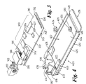
- a first part of a two-part housing of the optoelectronic module in this example constituting a base part 400 of the two-part housing, has a notional longitudinal central axis.
- the base part 400 comprises an inner side 402 profiled so as to provide a substantially planar surface 404 comprising a first raised portion 406 and a second raised portion 408, the first and second raised portions 406,408 defining a channel 410 which, in this example, is a blind channel closed by a partition wall 412.
- the blind channel 410 is intended for disposing the optoelectronic package 100 therein.
- a substantially complementarily shaped channel 414 is defined, in part, by a first side wall 416 and a second side wall 418.
- the complementarily shaped channel 414 becomes a complementarily shaped volume when the two-part housing is closed by a second, top, part (not shown) of the two-part housing.
- the complementarily shaped channel 414 is shaped so as to specifically receive the LC housing 200.
- the complementarily shaped channel 414 is sized to provide play between the interior of the complementarily shaped channel 414 and the LC housing 200.
- the complementarily shaped channel 414 comprises first and second recessed channels 434, 436 to receive the first and second protrusions 208.
- the first and second recessed channels 434, 436 are complementary with respect to the first and second protrusions 208.
- the first and second recessed channels 434, 436 are substantially perpendicular to the base part 400 to facilitate insertion of the LC housing 200 into the complementarily shaped channel 414.
- the first and second recessed channels 434, 436 are offset with respect to each other in a corresponding manner to that of the first and second protrusions 208.
- the first and second recessed channels 434, 436 comprise substantially vertical ribs to facilitate keying with adhesives.
- the complementarily shaped channel 414 can be provided with alternatively shaped features to co-operate with the locator features of the LC housing 200.
- the planar surface 404 comprises a raised annular portion 420 forming part of an internally threaded blind bore for receiving a screw (not shown) to secure the top part (not shown) of the two-part housing in order to close the housing.
- the outside surfaces of the base and top parts comprise fins 422 to assist heat dissipation by the two-part housing.
- a nylon gasket 424 can be disposed upon the raised annular portion 420 to aid alignment of the PCB 302 and stability to the complete assembly.
- Side walls 426 of the base part 400 of the two-part housing turn inwards towards each other at a distal end 428 of the optoelectronic module to form locator walls 430.
- the locator walls 430 together with a shallow end wall 432 and the top part of the two-part housing define a slot (not shown) through which an end portion 308 of the PCB 302 protrudes.
- the PCB 302 comprises locator shoulders 310 which co-operate with the locator walls 430 to prevent excessive protrusion of the PCB 302 beyond the slot, yet sufficiently to expose an edge connector 312 provided at the end portion 308 of the PCB 302.
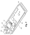
- the PCB 302 is soldered to the optoelectronic package 100 and an electromagnetic shielding gasket 500 is disposed between the optoelectronic package 100 and the LC housing 200.
- the optoelectronic package 100 is aligned with the LC housing 200, and subsequently with the PCB 302 as follows.
- the LC housing 200 and the optoelectronic package 100 are initially placed (step 600) on a first jig (not shown).
- the first jig holds and aids alignment of the above mentioned parts prior to insertion of the parts onto a second jig (not shown). Since the first jig is shaped so as to mimic the blind channel 410 and the complementarily shaped channel 414 of the two-part housing, whilst providing access to work on piece parts placed on the first jig, identical reference numerals and part names will be used to refer to corresponding parts of the first jig.
- the LC connector 200 is placed within the complementarily shaped channel 414 and the optoelectronic package 100 is placed in the blind channel 410 so that the optical connector 102 lies, at least in part, within the LC housing 200 and the ringed alignment feature 104 lie within and cooperates with the partitioned U-shaped channel 202 and an axial alignment and a correct positioning of the optical connector 102 within the LC housing 200 is obtained.
- the optoelectronic package 100 is displaced, rotated and/or jiggled, in the blind channel 410 and about a longitudinal axis of the optical connector 102 so as to ensure that the base 101 of the optoelectronic package 100 lies against the planar surface 404, i.e.
- step 602 rotational alignment of the optoelectronic package 100 is achieved.
- the optical connector 102 is fixed in position within the LC housing 200 using, for example, a known stake weld process (step 602).
- the second jig holds and aids alignment of the LC housing/optoelectronic package combination with the electronic assembly 300 prior to placing the LC housing 200, the optoelectronic package 100 and the electronic assembly 300 onto the base part 400 of the optoelectronic module. Since the second jig is shaped so as to mimic the base part 400 of the two-part housing, whilst providing access to work on the above parts placed on the second jig, identical reference numerals and part names will be used to refer to corresponding parts of the second jig.
- the electronic assembly 300 is then placed (step 604) on the second jig and the leads 106 are formed, i.e. bent into shape, and cut to an appropriate length and fed through respective apertures (not shown) in the PCB 302 for receiving the leads 106.
- the PCB 302 is displaced, or jiggled, i.e.
- the aperture 307 is disposed an appropriate distance from the end 309 of the PCB 302 so as to achieve minimal lateral translation of the end 309 of the PCB 302, whilst providing a sufficient ability to laterally translate the end of the PCB 302 adjacent the optoelectronic package 100.
- the required location of the edge connector 312 can thus be maintained whilst enabling attachment of the leads 106 to the PCB 302 in the light of the variety of slightly different positional locations that can be assumed by the optoelectronic package 100.
- the flexible conducting leads 16 are fixed to the PCB 302 using a known soldering process.
- the aligned and fixed LC housing 200, optoelectronic package 100 and electronic package 300 are then transferred from the second jig to the base part 400 of the optoelectronic module (step 606).
- the locator walls 430 and the nylon gasket 424 provide lateral and vertical constraints to the location of the PCB 302.
- the optoelectronic package 100 is adjusted in position so as to be mounted correctly within the blind channel 410.
- Such an adjustment in position of the optoelectronic package 100 coupled to the electronic package 300 is possible due to the freedom of movement provided by the independence of the LC housing 200 from the base part 400, i.e. the LC housing 200 is a separate part, within the complementarily shaped channel 414 that receives the LC housing 200.
- the LC housing 200 is bonded within the complementarily shaped channel 414 using an electrically conductive epoxy such as H20E as manufactured by Epoxy Technology, Inc. and the optoelectronic package 100 is bonded to the planar surface 404 within the blind channel 410, or to any suitable required intermediate layer disposed upon the planar surface 404 using a similar epoxy as already described above.
- the base part 400 with piece parts assembled thereon is then placed in an oven and the epoxy is cured (step 608) to fix the parts in place.
- top-part (not shown) of the two-part housing is brought together with the base part 400 of the two-part housing so as to close (step 610) the two-part housing.
- the top and base parts 400 are held together by a screw (not shown) passing through the top part and threaded into the internally threaded blind bore.
Description
- The present invention relates to a module apparatus for a fibre-optic communications system, the module being of the type, for example, that can be removably coupled to a Network Equipment Manufacturer's (NEMs) circuit board and replaced when such module fails. The present invention also relates to a method of aligning an optoelectronic package with a connector housing, for example, of the type forming part of the module apparatus.
- In an optical communications network, a known packaged optoelectronic module such as a transmitter, receiver or transceiver module typically comprises a housing containing an optical subassembly comprising, for example, an optoelectronic package having an optical connector for coupling to an external optical fibre for propagation of electromagnetic radiation to/from the network. The optoelectronic package has a laser device or a photodetector therein, and an array of flexible leads for communicating electrical signals to and from the interior of the optoelectronic package. The array of flexible conducting leads is typically coupled to a Printed Circuit Board (PCB) comprising known circuitry suitable for controlling the laser device or photodetector and to provide functionality to the module.
-
WO0077551 - In order to provide efficient coupling of electromagnetic radiation between the optical connector and an optoelectronic device located within the optoelectronic package, such as the laser device or the photodetector, an initial alignment process is necessary between the optical connector and active region of the optoelectronic device, for example a light emitting portion of the laser device in the case of the transmitter module or an absorbing portion of the photodetector in the case of the receiver module, or both for a tranceiver module. For an ideal coupling between the optical connector and the optoelectronic package, a central longitudinal axis associated with the optical connector should coincide with a centrally located axis passing through a wall of the optoelectronic package. However, the above initial alignment process typically results in the optical subassembly having an axial misalignment between the longitudinal axis of the optical connector and the central axis of the optoelectronic package. The amount of axial misalignment also varies between individual optical subassemblies according to the degree of positional adjustment of the optical connector necessary to align the optical connector with the optoelectronic device during the initial alignment process. Typically, the optical connector forms part of an industry standard connector, for example, a Lucent® Connector (LC) having a socket opening having a pre-defined configuration for receiving a complementarily shaped plug, the optical connector lying within the socket. The socket opening is integrally formed with the housing, the optical connector being fixed within the socket opening so as to maintain a fixed positional relationship between the socket opening and the optical connector. The inconsistent axial alignment between the individual optical connectors and the optoelectronic packages also results in the positional relationship between the optoelectronic packages and the PCBs varying from module to module. This inconsistent positional relationship between the optoelectronic packages and the PCBs complicates the design of a generic packaged optoelectronic module.
- In order to accommodate the variations in the positional relationship between the optoelectronic packages and the PCBs, it is known for the length of the array of flexible leads to vary in order to, where appropriate, bridge an increased wiring path between the optoelectronic packages and the PCBs. However, such an increase in electrical paths can result in the an increase in undesirable capacitive effects experienced by electrical signals using the extended array of leads.
- Additionally, where the laser diodes are housed within the optoelectronic packages, it is necessary to sink heat generated by the laser diodes. In addition to the relative position between the optoelectronic packages and the PCBs being inconsistent, the positional relationships between bases of the optoelectronic packages and housings containing the optoelectronic packages are also inconsistent, resulting in an inability to thermally couple the bases of the optoelectronic packages with the housings of the optelectronic modules in order to provide efficient heat removal from the optoelectronic package while in operation; efficient heat removal requires that the source of the heat dissipation, for example the optoelectronic package comprising the semiconductor laser device, to be disposed in intimate contact with the housing or other means of heat removal. Due to the inconsistent positional relationship between the bases of the optoelectronic packages and the housings, a variable gap typically exists between the housings and the optoelectronic packages.
- Without an efficient means of heat removal, the ambient temperature inside the packaged optoelectronic module can rise above the rated range of thermal operability recommended for components disposed upon the PCB and the optoelectronic device within the optoelectronic package, which can lead to malfunctions in the circuitry of the PCB and/or an unwanted variability in the laser device output characteristics or photodetector efficiency.
- According to the present invention, there is provided a module apparatus for a fibre-optic communications system, the apparatus comprising the features set forth in the claims that follow.
- Preferably, the optoelectronic device is a laser device and the housing further comprises means for maintaining the wavelength of the electromagnetic radiation emitted by the laser device at a desired wavelength. The means for maintaining the wavelength of the electromagnetic radiation at a desired wavelength to suit, for example, DWDM applications may be located within the optoelectronic package. More preferably, the means for maintaining the wavelength of the electromagnetic radiation at a desired wavelength of the electromagnetic radiation is a wavelength locker.
- Preferably, the connector housing is shaped and/or configured so as to define one half of an LC connection. More preferably, the half of the LC connection is an LC socket. Alternatively, the connector housing is shaped and/or configured so as to define one half of an MU connection.
- The housing may comprise an aperture to permit protrusion of an end of the electrical circuit board therethrough, the end of the electrical circuit board being distal from the optoelectronic package, the aperture being defined, in part, by a locator side wall for cooperating with the electrical circuit board so as to prevent excessive protrusion of the electrical circuit board beyond the aperture. Preferably, a locator shoulder is provided at the end of the electrical circuit board to cooperate with the locator side wall.
- Preferably, the electrical circuit board is arranged to cooperate with a pivot arrangement so as to pivot during assembly of the apparatus about a point provided by the pivot arrangement, thereby facilitating alignment of the electrical circuit board with respect to the optoelectronic package during assembly of the apparatus. More preferably, the electrical circuit board is arranged to cooperate with the pivot arrangement near the end of the electrical circuit board distal from the optoelectronic package. Very preferably, the electrical circuit board comprises an aperture formed therein located between a notional lateral centre line and the end of the electrical circuit board.
- The housing may comprise a channel for locating the optoelectronic package therein relative to the housing. The channel may be a blind channel.
- Preferably, the housing defines an internal volume and the electrical circuit board lies substantially within the internal volume, and the apparatus further comprises spacer means disposed adjacent the electrical circuit board so as to locate the electrical circuit board within the internal volume.
- Preferably, the housing defines a substantially complementarily shaped volume with respect to the connector housing, the connector housing being located within the complementarily shaped volume. More preferably, the complementarily shaped volume comprises locator features to at least hinder incorrect orientation of the connector housing within the complementarily shaped volume during assembly of the apparatus.
- The complementarily shaped volume may be partly defined by a first wall and a second wall, the first wall being shaped so as to provide a first locator feature and the second wall being shaped so as to provide a second locator feature, the first locator feature being offset with respect to the second locator feature. Preferably, the substantially complementarily shaped volume is shaped so as to provide a clearance for receiving adhesive between the connector housing and at least a portion of one of the first or second walls.
- Preferably, at least one of the locator features is configured so as to accommodate adhesive between the connector housing and the at least one of the locator features. More preferably, the at least one of the locator features is configured to facilitate keying between the at least one of the locator features and the adhesive.
- Preferably, the connector housing is arranged to comprise complementary locator features, the complementary locator features cooperating with the locator features. At least one of the complementary locator features may be configured so as to accommodate adhesive between the connector housing and the at least one of the complementary locator features. More preferably, the at least one of the complementary locator features is configured to facilitate keying between the at least one of the complementary locator features and the adhesive.
- The adhesive may be electrically conductive.
- It is thus possible to provide a module apparatus that reliably results in the optoelectronic package being disposed in thermal contact with a means for heat removal provided. A method of alignment of the optoelectronic package with the connector housing and the electrical circuit board can be used so as to obviate, or at least mitigate, unpredictable inductive effects, whilst ensuring that when mounting the optoelectronic package within the packaged optoelectronic module, the optoelectronic package is disposed in thermal contact with a means for heat removal provided. A generic packaged optoelectronic module is therefore provided.
- At least one embodiment of the present invention will now be described, by way of example only, with reference to the accompanying drawings, in which:
- Figure 1 is a schematic diagram of an optoelectronic package;
- Figure 2 is a schematic diagram of an LC housing;
- Figure 3 is a schematic diagram of the optoelectronic package of Figure 1 coupled to the LC housing of Figure 2 and an electrical circuit board;
- Figure 4 is a schematic diagram of a first half of a two-part outer housing;
- Figure 5 is a schematic diagram of a part-assembled apparatus comprising the parts of Figures 2, 3 and 4; and
- Figure 6 is a flow diagram of a method of assembly of the module apparatus as shown, in part, in Figure 5.
- Throughout the following description identical reference numerals will be used to identify like parts.
- Referring to Figure 1, an
optoelectronic package 100 having abase 101 forms a part of a packaged optoelectronic module (not shown) and comprises anoptical connector 102 constituting a first part of a coupling, theoptical connector 102 being capable of receiving a ferrule connector. Theoptical connector 102 comprises a number of ringed alignment features 104 along its length and has a first end coupled to a first side of theoptoelectronic package 100 which comprises, on a second side, an array offlexible connecting leads 106. Disposed within theoptoelectronic package 100 is an optoelectronic device (not shown) such as a laser device to transmit electromagnetic radiation (not shown) from theoptoelectronic package 100 within the optoelectronic module to an optical communications system connected to the optoelectronic module by means of, for example, a fibre-optic patch cord (not shown) connected to the optical communications system and coupled to a second end of theoptical connector 102. - The module apparatus and, for example, in particular the
optoelectronic package 100 can contain means for maintaining a wavelength of electromagnetic radiation emitted by the laser device, for example, a wavelength locker. - Referring to Figure 2, a connector housing, such as an
LC housing 200, comprises a partitioned U-shapedchannel 202 to receive theringed alignment features 104 of theoptical connector 102 of Figure 1. TheLC housing 200 further comprises a profiledopening 204 to receive a second part of the coupling, for example an LC plug coupled to a fibre-optic patch cord (not shown) which is ultimately coupleable to the second end of theoptical connector 102 of Figure 1. Afirst side 206 of theLC housing 200 comprises afirst protrusion 208 and asecond side 210 of theLC housing 200 comprises a second protrusion (not shown), thefirst protrusion 208 being offset with respect to the second protrusion. In this example, the first andsecond protrusions 208 are profiled, for example their surfaces comprise striped grooves to enhance keying of the protrusions with adhesives. The first andsecond protrusions 208 constitute locator features for ensuring correct orientation of theLC housing 200 during assembly thereof. It should be appreciated that alternatives to the protrusions exist and theLC housing 200 can have other features, for example, recesses to achieve the same effect. - Referring to Figure 3, the
optical connector 102 is coupled to theLC housing 200 by a known laser stake welding technique, and the array of flexible connectingleads 106 are coupled to anelectronic assembly 300 by, for example, a known solder process. Theelectronic assembly 300 comprises a Printed Circuit Board (PCB) 302 populated bycomponents 304 arranged to, for example, drive the optoelectronic device within theoptoelectronic package 100 and means for cooling the optoelectronic device, for example a thermoelectriccooler device 306. ThePCB 302 comprises acircular aperture 307 located between a notional lateral centre line (not shown) and anend 309 of thePCB 302 distal from an end thereof to be coupled adjacent theoptoelectronic package 100.
Referring to Figure 4, a first part of a two-part housing of the optoelectronic module, in this example constituting abase part 400 of the two-part housing, has a notional longitudinal central axis. Thebase part 400 comprises aninner side 402 profiled so as to provide a substantiallyplanar surface 404 comprising a first raisedportion 406 and a second raisedportion 408, the first and second raised portions 406,408 defining achannel 410 which, in this example, is a blind channel closed by a partition wall 412. Theblind channel 410 is intended for disposing theoptoelectronic package 100 therein. At a first, proximal, end of thebase part 400, a substantially complementarily shapedchannel 414 is defined, in part, by afirst side wall 416 and asecond side wall 418. The complementarily shapedchannel 414 becomes a complementarily shaped volume when the two-part housing is closed by a second, top, part (not shown) of the two-part housing. The complementarily shapedchannel 414 is shaped so as to specifically receive theLC housing 200. However, the complementarily shapedchannel 414 is sized to provide play between the interior of the complementarily shapedchannel 414 and theLC housing 200. - The complementarily shaped
channel 414 comprises first and second recessedchannels second protrusions 208. The first and second recessedchannels second protrusions 208. In this example, the first and second recessedchannels base part 400 to facilitate insertion of theLC housing 200 into the complementarily shapedchannel 414. The first and second recessedchannels second protrusions 208. The first and second recessedchannels channels channel 414 can be provided with alternatively shaped features to co-operate with the locator features of theLC housing 200. - The
planar surface 404 comprises a raisedannular portion 420 forming part of an internally threaded blind bore for receiving a screw (not shown) to secure the top part (not shown) of the two-part housing in order to close the housing. The outside surfaces of the base and top parts comprisefins 422 to assist heat dissipation by the two-part housing. Anylon gasket 424 can be disposed upon the raisedannular portion 420 to aid alignment of thePCB 302 and stability to the complete assembly.Side walls 426 of thebase part 400 of the two-part housing turn inwards towards each other at adistal end 428 of the optoelectronic module to formlocator walls 430. Thelocator walls 430, together with ashallow end wall 432 and the top part of the two-part housing define a slot (not shown) through which anend portion 308 of thePCB 302 protrudes. ThePCB 302 comprises locator shoulders 310 which co-operate with thelocator walls 430 to prevent excessive protrusion of thePCB 302 beyond the slot, yet sufficiently to expose anedge connector 312 provided at theend portion 308 of thePCB 302. - Referring to Figure 5, the
PCB 302 is soldered to theoptoelectronic package 100 and anelectromagnetic shielding gasket 500 is disposed between theoptoelectronic package 100 and theLC housing 200. - The
optoelectronic package 100 is aligned with theLC housing 200, and subsequently with thePCB 302 as follows. - Referring to Figure 6, the
LC housing 200 and theoptoelectronic package 100 are initially placed (step 600) on a first jig (not shown). The first jig holds and aids alignment of the above mentioned parts prior to insertion of the parts onto a second jig (not shown). Since the first jig is shaped so as to mimic theblind channel 410 and the complementarily shapedchannel 414 of the two-part housing, whilst providing access to work on piece parts placed on the first jig, identical reference numerals and part names will be used to refer to corresponding parts of the first jig. - Firstly, the
LC connector 200 is placed within the complementarily shapedchannel 414 and theoptoelectronic package 100 is placed in theblind channel 410 so that theoptical connector 102 lies, at least in part, within theLC housing 200 and the ringedalignment feature 104 lie within and cooperates with the partitionedU-shaped channel 202 and an axial alignment and a correct positioning of theoptical connector 102 within theLC housing 200 is obtained. Theoptoelectronic package 100 is displaced, rotated and/or jiggled, in theblind channel 410 and about a longitudinal axis of theoptical connector 102 so as to ensure that thebase 101 of theoptoelectronic package 100 lies against theplanar surface 404, i.e. rotational alignment of theoptoelectronic package 100 is achieved. Following the correct alignment and positioning of theoptical connector 102 within theLC housing 200, theoptical connector 102 is fixed in position within theLC housing 200 using, for example, a known stake weld process (step 602). - The
LC housing 200 and theoptoelectronic package 100, now fixed to theLC housing 200, are transferred to the second jig (not shown). The second jig holds and aids alignment of the LC housing/optoelectronic package combination with theelectronic assembly 300 prior to placing theLC housing 200, theoptoelectronic package 100 and theelectronic assembly 300 onto thebase part 400 of the optoelectronic module. Since the second jig is shaped so as to mimic thebase part 400 of the two-part housing, whilst providing access to work on the above parts placed on the second jig, identical reference numerals and part names will be used to refer to corresponding parts of the second jig. - Consequently, the
electronic assembly 300 is then placed (step 604) on the second jig and theleads 106 are formed, i.e. bent into shape, and cut to an appropriate length and fed through respective apertures (not shown) in thePCB 302 for receiving theleads 106. ThePCB 302 is displaced, or jiggled, i.e. in a second plane substantially parallel with theplanar surface 404 so as to ensure thePCB 302 now attached to theoptoelectronic package 100 by theleads 106, is suitably aligned with respect to the notional central longitudinal axis of the base part 400so as to ensure an optimum positional relationship between theedge connector 312 and the notional central longitudinal axis, thereby enabling proper connection of theedge connector 312 to another circuit board arranged to receive theedge connector 312. It should be appreciated that theaperture 307 is disposed an appropriate distance from theend 309 of thePCB 302 so as to achieve minimal lateral translation of theend 309 of thePCB 302, whilst providing a sufficient ability to laterally translate the end of thePCB 302 adjacent theoptoelectronic package 100. The required location of theedge connector 312 can thus be maintained whilst enabling attachment of theleads 106 to thePCB 302 in the light of the variety of slightly different positional locations that can be assumed by theoptoelectronic package 100. - Once suitable alignment tolerances are achieved, the flexible conducting leads 16 are fixed to the
PCB 302 using a known soldering process. - The aligned and fixed
LC housing 200,optoelectronic package 100 andelectronic package 300 are then transferred from the second jig to thebase part 400 of the optoelectronic module (step 606). Thelocator walls 430 and thenylon gasket 424 provide lateral and vertical constraints to the location of thePCB 302. Theoptoelectronic package 100 is adjusted in position so as to be mounted correctly within theblind channel 410. Such an adjustment in position of theoptoelectronic package 100 coupled to theelectronic package 300 is possible due to the freedom of movement provided by the independence of theLC housing 200 from thebase part 400, i.e. theLC housing 200 is a separate part, within the complementarily shapedchannel 414 that receives theLC housing 200. Once suitable alignment tolerances are met, theLC housing 200 is bonded within the complementarily shapedchannel 414 using an electrically conductive epoxy such as H20E as manufactured by Epoxy Technology, Inc. and theoptoelectronic package 100 is bonded to theplanar surface 404 within theblind channel 410, or to any suitable required intermediate layer disposed upon theplanar surface 404 using a similar epoxy as already described above. Thebase part 400 with piece parts assembled thereon is then placed in an oven and the epoxy is cured (step 608) to fix the parts in place. - Finally, the top-part (not shown) of the two-part housing is brought together with the
base part 400 of the two-part housing so as to close (step 610) the two-part housing. The top andbase parts 400 are held together by a screw (not shown) passing through the top part and threaded into the internally threaded blind bore. - Although, in the above examples, reference has been made to LC connections, it should be appreciated that other connections are equally applicable, for example, an MU connection.
Claims (18)
- A module apparatus for a fibre-optic communications system, the apparatus comprising:a housing assembly having a base part (400),an optoelectronic package (100) having at least one optoelectronic device therein, the optoelectronic package being disposed within the base part of the housing assembly; the optoelectronic package comprising a first part of a coupling (102) attached thereto, the coupling being arranged to receive a ferrule connector;an electrical circuit board electrically coupled to the optoelectronic device within the optoelectronic package (100);a connector housing (200),wherein at least a portion of the first part of the coupling is substantially fixedly located within the connector housing (200);
characterized in that the connector housing is received within a complementary shaped channel (414) disposed on the base part of the housing assembly, the connector housing (200) being an independent part with respect to at least a part of the housing assembly; and
the base part (400) of the housing assembly comprises a further channel (410) locating the optoelectronic package therein. - An apparatus as claimed in claim 1, wherein the connector housing (200) is shaped and/or configured so as to define one half of an LC connection.
- An apparatus as claimed in claim 2, wherein the half of the LC connection is an LC socket.
- An apparatus as claimed in one of the preceding claims, wherein the complementary shaped channel (414) is integrally formed with the base part (400) of the housing assembly.
- An apparatus as claimed in claim 5, wherein the base part of the housing (400) comprises an aperture to permit protrusion of an end (308) of the electrical circuit board (302) being distal from the optoelectronic package (100), the aperture being defined, in part, by a locator side wall (426) for cooperating with the electrical circuit board (302) so as to prevent excessive protrusion of the electrical circuit board (302) beyond the aperture.
- An apparatus as claimed in claim 6, wherein a locator shoulder (430) is provided at the end of the electrical circuit board (302) to cooperate with the locator side wall (426).
- An apparatus as claimed in claims 5-7, wherein the electrical circuit board (302) is arranged to cooperate with a pivot arrangement so as to pivot during assembly of the apparatus about a point provided by the pivot arrangement, thereby facilitating alignment of the electrical circuit board (302) with respect to the optoelectronic package (100) during assembly of the apparatus.
- An apparatus as claimed in claim 8, wherein the electrical circuit board (302) is arranged to cooperate with the pivot arrangement near the end (309) of the electrical circuit board distal from the optoelectronic package (100).
- An apparatus as claimed in claim 9, wherein the electrical circuit board (302) comprises an aperture (307) formed therein located between a notional lateral centre line and the end (309) of the electrical circuit board.
- An apparatus as claimed in claims 5-10, wherein the base part of the housing (400) defines an internal volume and the electrical circuit board (302) lies substantially within the internal volume, and wherein the apparatus further comprises a spacer disposed adjacent the electrical circuit board so as to locate the electrical circuit board within the internal volume.
- An apparatus as claimed in any one of the preceding claims, wherein the base part of the housing (400) defines a substantially complementarily shaped volume with respect to the connector housing (200), the connector housing being located within the complementarily shaped volume.
- An apparatus as claimed in claim 12, wherein the complementarily shaped volume comprises locator features (434, 436) to at least hinder incorrect orientation of the connector housing (200) within the complementarily shaped volume during assembly of the apparatus.
- An apparatus as claimed in claim 13, wherein the connector housing (200) is arranged to comprise complementary connector locator features (208, 210), the complementary connector locator features cooperating with the volume locator features (434, 436).
- An apparatus as claimed in claim 13-14, wherein the complementarily shaped volume is partly defined by a first wall (416) and a second wall (418), the first wall being shaped so as to provide a first volume locator feature (436) and the second wall being shaped so as to provide a second volume locator feature (434), the first volume locator feature being offset with respect to the second volume locator feature.
- An apparatus as claimed in claim 15, wherein the substantially complementarily shaped volume is shaped so as to provide a clearance for receiving adhesive between the connector housing (200) and at least a portion of one of the first or second walls (416, 418).
- An apparatus as claimed in claim 16, wherein the at least one of the volume locator features (434, 436) is configured to facilitate keying between the at least one of the connector locator features (208, 210) and/or the adhesive.
- An apparatus as claimed in claims 16/17, wherein the adhesive is electrically conductive.
- An apparatus as claimed in claim 1, wherein the complementary shaped channel (414) is shaped so as to facilitate the close thermal contact between the optoelectronic package (100) and the base part of the housing assembly (400).
Priority Applications (3)
| Application Number | Priority Date | Filing Date | Title |
|---|---|---|---|
| DE60224359T DE60224359D1 (en) | 2002-03-27 | 2002-03-27 | module device |
| EP02252208A EP1348989B1 (en) | 2002-03-27 | 2002-03-27 | Module apparatus |
| US10/396,236 US6929407B2 (en) | 2002-03-27 | 2003-03-25 | Module apparatus and method of alignment |
Applications Claiming Priority (1)
| Application Number | Priority Date | Filing Date | Title |
|---|---|---|---|
| EP02252208A EP1348989B1 (en) | 2002-03-27 | 2002-03-27 | Module apparatus |
Publications (2)
| Publication Number | Publication Date |
|---|---|
| EP1348989A1 EP1348989A1 (en) | 2003-10-01 |
| EP1348989B1 true EP1348989B1 (en) | 2008-01-02 |
Family
ID=27798914
Family Applications (1)
| Application Number | Title | Priority Date | Filing Date |
|---|---|---|---|
| EP02252208A Expired - Lifetime EP1348989B1 (en) | 2002-03-27 | 2002-03-27 | Module apparatus |
Country Status (3)
| Country | Link |
|---|---|
| US (1) | US6929407B2 (en) |
| EP (1) | EP1348989B1 (en) |
| DE (1) | DE60224359D1 (en) |
Families Citing this family (19)
| Publication number | Priority date | Publication date | Assignee | Title |
|---|---|---|---|---|
| TWI244278B (en) | 2004-06-04 | 2005-11-21 | Ind Tech Res Inst | Optical transceiver module |
| US20060002666A1 (en) * | 2004-06-30 | 2006-01-05 | Ice Donald A | Shaped lead assembly for optoelectronic devices |
| US7476905B2 (en) * | 2004-10-25 | 2009-01-13 | Finisar Corporation | Securing a transistor outline can within an optical component |
| DE202006006359U1 (en) * | 2006-04-20 | 2006-07-13 | Rosenberger Hochfrequenztechnik Gmbh & Co. Kg | Potential-free housing feedthrough |
| US7547149B2 (en) | 2006-12-19 | 2009-06-16 | Finisar Corporation | Optical connector latch assembly for an optoelectronic module |
| US7484987B2 (en) | 2006-12-19 | 2009-02-03 | Finisar Corporation | Latch assembly for an optoelectronic module |
| US7625137B2 (en) | 2006-12-19 | 2009-12-01 | Finisar Corporation | Communications device |
| US7845862B2 (en) * | 2006-12-19 | 2010-12-07 | Finisar Corporation | Communications device |
| US7646615B2 (en) * | 2006-12-19 | 2010-01-12 | Finisar Corporation | Electromagnetic inferference shield for an optoelectronic module |
| US7543995B2 (en) * | 2006-12-19 | 2009-06-09 | Finisar Corporation | Optical subassembly connector block for an optoelectronic module |
| IT1390779B1 (en) * | 2008-07-03 | 2011-09-23 | St Microelectronics Srl | PHOTOVOLTAIC DEVICE WITH CONCENTRATION AND SPECTAL DISTRIBUTION OF CAPTATA RADIATION |
| US8821039B2 (en) | 2009-10-29 | 2014-09-02 | Sumitomo Electric Industries, Ltd. | Optical transceiver having optical receptacle arranged diagonally to longitudinal axis |
| WO2011052802A2 (en) | 2009-10-29 | 2011-05-05 | Sumitomo Electric Industries, Ltd. | Pluggable optical transceiver and method for manufacturing the same |
| US9052477B2 (en) | 2009-10-29 | 2015-06-09 | Sumitomo Electric Industries, Ltd. | Optical transceiver with inner fiber set within tray securing thermal path from electronic device to housing |
| US9351420B2 (en) * | 2011-11-14 | 2016-05-24 | Rockwell Automation Technologies, Inc. | Systems and methods for manufacturing industrial automation drives |
| US9874688B2 (en) | 2012-04-26 | 2018-01-23 | Acacia Communications, Inc. | Co-packaging photonic integrated circuits and application specific integrated circuits |
| SG10201805058VA (en) | 2014-10-29 | 2018-07-30 | Acacia Communications Inc | Optoelectronic ball grid array package with fiber |
| JP6957894B2 (en) * | 2017-02-22 | 2021-11-02 | 日本電気株式会社 | Pluggable optical module and pluggable optical module connection structure |
| CN112888255A (en) * | 2021-01-20 | 2021-06-01 | 四川中科友成科技有限公司 | Controllable heat dissipation system and controllable heat dissipation method based on semiconductor refrigeration |
Family Cites Families (10)
| Publication number | Priority date | Publication date | Assignee | Title |
|---|---|---|---|---|
| US5151961A (en) * | 1992-02-20 | 1992-09-29 | Northern Telecom Limited | Ferrule alignment assembly for blind mating optical fiber connector |
| US5325454A (en) * | 1992-11-13 | 1994-06-28 | International Business Machines, Corporation | Fiber optic connector housing |
| US5329604A (en) * | 1993-02-11 | 1994-07-12 | International Business Machines Corporation | Optical fiber coupling device and optoelectronic system utilizing same |
| JP3549659B2 (en) * | 1996-02-19 | 2004-08-04 | 富士通株式会社 | Method for manufacturing optical waveguide device |
| JPH10206675A (en) * | 1997-01-24 | 1998-08-07 | Ngk Insulators Ltd | Reel for optical fiber coil |
| US6299362B1 (en) * | 1998-04-22 | 2001-10-09 | Stratos Lightwave, Inc. | High speed optical interface converter module having mounting halves |
| EP0973051A1 (en) * | 1998-07-17 | 2000-01-19 | Siecor Operations, LLC | Pin retainer and associated method for assembling a fiber optic connector |
| US7090509B1 (en) * | 1999-06-11 | 2006-08-15 | Stratos International, Inc. | Multi-port pluggable transceiver (MPPT) with multiple LC duplex optical receptacles |
| DE10001680C1 (en) * | 2000-01-12 | 2001-08-23 | Infineon Technologies Ag | Multi-channel optical coupling arrangement |
| US6692159B2 (en) * | 2001-04-14 | 2004-02-17 | E20 Communications, Inc. | De-latching mechanisms for fiber optic modules |
-
2002
- 2002-03-27 DE DE60224359T patent/DE60224359D1/en not_active Expired - Lifetime
- 2002-03-27 EP EP02252208A patent/EP1348989B1/en not_active Expired - Lifetime
-
2003
- 2003-03-25 US US10/396,236 patent/US6929407B2/en not_active Expired - Lifetime
Also Published As
| Publication number | Publication date |
|---|---|
| US6929407B2 (en) | 2005-08-16 |
| DE60224359D1 (en) | 2008-02-14 |
| EP1348989A1 (en) | 2003-10-01 |
| US20030185525A1 (en) | 2003-10-02 |
Similar Documents
| Publication | Publication Date | Title |
|---|---|---|
| EP1348989B1 (en) | Module apparatus | |
| US7435014B2 (en) | Methods for assembling an optical transceiver | |
| US7455463B2 (en) | High density array of optical transceiver modules | |
| JP5943372B2 (en) | Compact high-speed optical module | |
| US7367720B2 (en) | Optical transceiver with optical subassemblies optionally fixed to housing | |
| US20060032665A1 (en) | Single layer flex circuit | |
| US7334948B2 (en) | Modular optical device with component insert | |
| US20030206703A1 (en) | Transmitters, receivers, and transceivers including an optical bench | |
| US7284916B2 (en) | Dual stage modular optical devices with insert digital diagnostics component | |
| US20070009213A1 (en) | Optoelectronic assembly with heat sink | |
| US7805084B2 (en) | Dual stage modular optical devices | |
| JP2005227783A (en) | Optical data link having receptacle attached to housing by structure movable thereto | |
| KR20050013508A (en) | Modular optical transceiver | |
| US9063310B2 (en) | Optical transceiver implementing with flexible printed circuit connecting optical subassembly to circuit board | |
| US7463830B2 (en) | Modular optical transmitter for WWDM transceivers | |
| US7359642B2 (en) | Modular optical receiver | |
| US20040091268A1 (en) | Transmitter optical sub-assembly | |
| US20190361181A1 (en) | Heat dissipation structure of horizontal optical-communication sub-assembly | |
| US7344319B2 (en) | Shaped lead assembly for optoelectronic devices | |
| US10371909B2 (en) | Thermal interface | |
| US20050185963A1 (en) | Optical transceiver with variably positioned insert | |
| US6530699B1 (en) | Dual channel device having two optical sub-assemblies | |
| US6999644B1 (en) | Discrete optoelectric package | |
| WO2011152555A1 (en) | Optical transceiver with block to dissipate heat from tosa to cover | |
| JP2010008588A (en) | Optical transceiver |
Legal Events
| Date | Code | Title | Description |
|---|---|---|---|
| PUAI | Public reference made under article 153(3) epc to a published international application that has entered the european phase |
Free format text: ORIGINAL CODE: 0009012 |
|
| AK | Designated contracting states |
Kind code of ref document: A1 Designated state(s): AT BE CH CY DE DK ES FI FR GB GR IE IT LI LU MC NL PT SE TR |
|
| AX | Request for extension of the european patent |
Extension state: AL LT LV MK RO SI |
|
| 17P | Request for examination filed |
Effective date: 20040401 |
|
| AKX | Designation fees paid |
Designated state(s): DE GB |
|
| 17Q | First examination report despatched |
Effective date: 20050826 |
|
| RAP1 | Party data changed (applicant data changed or rights of an application transferred) |
Owner name: AVAGO TECHNOLOGIES FIBER IP (SINGAPORE) PTE. LTD. |
|
| GRAP | Despatch of communication of intention to grant a patent |
Free format text: ORIGINAL CODE: EPIDOSNIGR1 |
|
| RTI1 | Title (correction) |
Free format text: MODULE APPARATUS |
|
| GRAS | Grant fee paid |
Free format text: ORIGINAL CODE: EPIDOSNIGR3 |
|
| GRAA | (expected) grant |
Free format text: ORIGINAL CODE: 0009210 |
|
| AK | Designated contracting states |
Kind code of ref document: B1 Designated state(s): DE GB |
|
| REG | Reference to a national code |
Ref country code: GB Ref legal event code: FG4D |
|
| REF | Corresponds to: |
Ref document number: 60224359 Country of ref document: DE Date of ref document: 20080214 Kind code of ref document: P |
|
| PLBE | No opposition filed within time limit |
Free format text: ORIGINAL CODE: 0009261 |
|
| STAA | Information on the status of an ep patent application or granted ep patent |
Free format text: STATUS: NO OPPOSITION FILED WITHIN TIME LIMIT |
|
| 26N | No opposition filed |
Effective date: 20081003 |
|
| PG25 | Lapsed in a contracting state [announced via postgrant information from national office to epo] |
Ref country code: DE Free format text: LAPSE BECAUSE OF FAILURE TO SUBMIT A TRANSLATION OF THE DESCRIPTION OR TO PAY THE FEE WITHIN THE PRESCRIBED TIME-LIMIT Effective date: 20080403 |
|
| REG | Reference to a national code |
Ref country code: GB Ref legal event code: 732E Free format text: REGISTERED BETWEEN 20130725 AND 20130731 |
|
| PGFP | Annual fee paid to national office [announced via postgrant information from national office to epo] |
Ref country code: GB Payment date: 20150226 Year of fee payment: 14 |
|
| GBPC | Gb: european patent ceased through non-payment of renewal fee |
Effective date: 20160327 |
|
| PG25 | Lapsed in a contracting state [announced via postgrant information from national office to epo] |
Ref country code: GB Free format text: LAPSE BECAUSE OF NON-PAYMENT OF DUE FEES Effective date: 20160327 |