EP1347478A2 - Micromachined parallel-plate variable capacitor with plate suspension - Google Patents
Micromachined parallel-plate variable capacitor with plate suspension Download PDFInfo
- Publication number
- EP1347478A2 EP1347478A2 EP02023307A EP02023307A EP1347478A2 EP 1347478 A2 EP1347478 A2 EP 1347478A2 EP 02023307 A EP02023307 A EP 02023307A EP 02023307 A EP02023307 A EP 02023307A EP 1347478 A2 EP1347478 A2 EP 1347478A2
- Authority
- EP
- European Patent Office
- Prior art keywords
- top plate
- plate
- capacitor
- springs
- outer portion
- Prior art date
- Legal status (The legal status is an assumption and is not a legal conclusion. Google has not performed a legal analysis and makes no representation as to the accuracy of the status listed.)
- Granted
Links
Images



Classifications
-
- H—ELECTRICITY
- H01—ELECTRIC ELEMENTS
- H01G—CAPACITORS; CAPACITORS, RECTIFIERS, DETECTORS, SWITCHING DEVICES, LIGHT-SENSITIVE OR TEMPERATURE-SENSITIVE DEVICES OF THE ELECTROLYTIC TYPE
- H01G5/00—Capacitors in which the capacitance is varied by mechanical means, e.g. by turning a shaft; Processes of their manufacture
- H01G5/16—Capacitors in which the capacitance is varied by mechanical means, e.g. by turning a shaft; Processes of their manufacture using variation of distance between electrodes
Definitions
- the present invention relates to capacitors for use in electrical circuits and the like, and more particularly, to a variable capacitor that is adapted for fabrication using micromachining.
- Parallel plate capacitors having a capacitance that depends on the potential difference between the plates are well known in the electrical arts.
- the devices typically consist of a fixed bottom plate and a movable top plate that is held over the bottom plate with the aid of a number of springs. As the potential difference between the plates is increased, the top plate is pulled toward the bottom plate by the electrostatic forces against the restoring forces provided by the spring system.
- Variable capacitors of this type are described in Darrin J. Young and Bernhard E. Boser, "A Micromachined Variable Capacitor for Monolithic Low-Noise VCOs," Technical Digest of Solid-State Sensor and Actuator Workshop, 1996, pp.
- variable capacitors in mass-produced electronics depends on the reproducibility of the capacitors, particularly the voltage versus capacitance function provided by each capacitor.
- the spring forces provided by the suspension springs must be repeatable from device to device. This, in turn, requires that the stress in the springs in the absence of an applied voltage be repeatable and, for a given voltage, be repeatable during operation.
- a tensile or compressive stress on the springs makes the effective spring constant higher or lower, respectively, and hence, alters the capacitance as a function of voltage curve.
- the top plate is typically constructed from a conducting film that is deposited using conventional integrated circuit fabrication techniques. Stress in this film can translate into stress in the springs if the film cannot change size to relieve the stress. As a practical matter, stress in the film or films that form the top capacitor plate is very difficult to control for a number of reasons. First, during fabrication, there is normally residual stress in the film or films that make up the top plate and spring. Second, during packaging, the die-attachment material applies stress to the bottom of the substrate.
- the temperature varies.
- the substrate e.g., silicon or glass
- the package usually do not have the same thermal expansion rate as the films that make up the top plate.
- a change in temperature results in a variable stress in the plate-spring structure.
- TCE thermal coefficient of expansion
- the problems caused by temperature fluctuations can be reduced by using the same material for the top plate as is used for the underlying substrate, and hence, reduce the mismatch in TCE between the two structures.
- silicon has a much higher resistivity than metals, and hence, such capacitors are poorly suited for capacitors in high-frequency applications.
- the present invention is a capacitor having a bottom plate, a top plate and a support connected to the center portion of the top plate for positioning the top plate over the bottom plate and separated therefrom by a gap.
- the outer portion of the top plate moves relative to the bottom plate when a potential is applied between the top and bottom plates.
- the outer portion of the top plate may be connected to the central portion of the top plate by a plurality of springs such that the movement of the top plate relative to the bottom plate is accommodated by bending at least one of the springs.
- the capacitor may also include an insulating layer between the top and bottom plates disposed so as to prevent the top plate from shorting to the bottom plate.
- a spacer for setting the minimum distance between the outer portion of the top plate and the bottom plate may also be included.
- the springs are shaped to relieve thermal stress between the outer portion of the top plate and the center portion of the top plate.
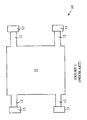
- Variable capacitor 10 has a top plate 11 that is suspended by springs 12. Each spring is attached to a support 13 at one end and plate 11 at the other end. The supports are also attached to the underlying substrate. If the substrate has a different rate of thermal expansion from that of the support, temperature changes will induce stresses in the springs. If the size of top plate 11 tries to increase relative to the spacing of the supports, it can be seen that the springs will be compressed. Similarly, if the size of the top plate tries to decrease relative to the spacing of the supports, the springs will be stretched. As noted above, such stretching or compression alters the effective spring constant, and hence, changes the amount of displacement that is obtained for a given applied voltage.
- the present invention is based on the observation that the prior art devices suspend the top plate at its periphery using multiple supports, and hence, any changes in the size of the top plate relative to the support placing gives rise to a stress that must be taken up either by the top plate or the springs.
- the present invention avoids these problems by utilizing an arrangement in which the top plate is supported substantially at its center by springs that are attached to a support, and hence, the top plate is free to expand or contract with changes in temperature.
- the present invention is much less sensitive to stresses induced in the fabrication processes, since using the single center support prevents such stresses from changing the size of the top plate.
- stresses that alter the size of the top plate do not induce stresses in the springs.
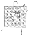
- FIG. 2 is a top view of capacitor 20.
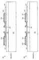
- Figure 3 is a cross-sectional view of capacitor 20 taken through line 21-22.
- Capacitor 20 is constructed on a substrate 30 on which a bottom plate 29 has been deposited.
- the top plate 23 is connected substantially at its center to a support 25 by springs 24.
- a protrusion 27 is provided in the top plate. Protrusion 27 sets the maximum displacement of top plate 23.
- An insulating layer 33 prevents shorts between top plate 23 and bottom plate 29 when the top plate moves downward.
- the center support 25 is sufficiently large to act as a bond pad for the top plate.
- a bond pad for the bottom plate is shown at 31.
- the support, springs and top plate are all made of the same material by patterning a metal layer such that the holes shown at 34 define the springs.
- the springs can be patterned such that a change in the length of the springs does not significantly change the spring constant.
- Figure 4 is a top view of a capacitor 40 according to another embodiment of the present invention. To simplify the discussion, those features shown in Figure 4 that serve the same function as features shown in Figures 2 and 3 have been given the same numeric designations.
- the springs 41 are patterned to have a "z" shape. This provides the desired stress relief.
- the top plate also includes a plurality of holes such as hole 36 shown in Figure 2. As will be explained in more detail below, these holes provide access to the layer under the top plate during the fabrication process such that material can be etched from under the top plate.
- the capacitor is typically constructed on a high-resistivity silicon wafer 101 on which an isolation layer 102 has been deposited.
- Isolation layer 102 is preferably low-temperature oxide (LTO).
- LTO low-temperature oxide
- a nonconducting substrate such as glass or plastic can be used.
- a gold layer is then deposited and patterned to form the bottom electrode 103 of capacitor 100 and a base 104 for the center support of the capacitor.
- a silicon nitride layer 105 and a phosphosilicate glass (PSG) sacrificial layer 106 are then deposited and patterned over the patterned gold layer.
- PSG phosphosilicate glass
- sacrificial layer 106 is then selectively etched to form depressions 107. These depressions determine the shape of the protrusions 27 discussed above.
- a second gold layer 110 is then deposited and patterned on top of sacrificial layer 106 to form the top electrode and the remainder of the support as shown in Figure 7.
- Gold layer 110 is selectively etched to form the springs and the holes.
- the sacrificial layer is then removed by a 10:1 BHF etch that reaches the sacrificial layer through the holes. This leaves the top plate of the capacitor suspended over the bottom electrode by the springs discussed above as shown in Figure 8.
- FIGS. 9 and 10 are cross-sectional views of a capacitor 150 during different stages of its construction. Capacitor 150 utilizes one of these alternative support designs.
- Capacitor 150 differs from capacitor 100 discussed above in that the base104 of the support has been omitted. Hence, the nitride layer 121 and sacrificial layer 122 extend under the central region of the top plate 125 as shown in Figure 9.
- the top plate is patterned to provide the holes that define the springs and provide the access for the etchant, no holes are provided under the central region of the top plate. Accordingly, the PSG sacrificial layer will etch much more slowly under the central region. The etch is timed such that a PSG support 126 remains under the center of top plate 125 after the PSG layer has been etched under the remainder of top plate 125 as shown in Figure 10.
- protrusion 27 as shown in Figure 2 in the top plate to set the minimum distance between the top and bottom plates.
- other forms of spacers may also be utilized.
- a similar protrusion can be deposited on the bottom plate before depositing the nitride insulating layer.
- an insulating "bump" can be deposited between the top and bottom plates to prevent the two plates from shorting. In this case, the nitride insulating layer can be omitted.
- the top plate has been assumed to be rigid with the springs providing the flexibility that allows the top plate to bend downward toward the bottom plate in response to a potential being applied between the top and bottom plates.
- the resultant capacitance-versus-potential curve is far from being linear.
- the capacitance can only be controllably increased by about 50%. This limitation is due to the electrostatic force nonlinearly increasing more rapidly than the linear restoring spring force as the top plate moves downward. When the electrostatic force exceeds the spring force, the top plate suddenly snaps down toward the bottom plate.
- the linearity of the capacitance curve can be increased by using a top plate that is flexible.
- the region of the top plate away from the springs will flex downward more than the springs alone allow, giving greater capacitance change at low voltage.
- the rest of the top plate can continue to move downward, allowing the capacitance to continue to increase more than 50%.
- the dynamic range is improved.
- the linearity of the capacitance curve with applied voltage is also improved.
- the flexibility of the top plate can be controlled by controlling the thickness of the material used to construct the plate.
- the flexibility of the top plate can also be increased by dividing the top plate into a plurality of regions that are connected to one another by springs.
- Figure 11 is a top view of a capacitor 200 according to another embodiment of the present invention.
- the etch holes shown in the previous embodiments have been omitted from the figure.
- the top plate 241 is suspended substantially at its center over the bottom plate 242 by a support 230 in a manner analogous to that discussed above.
- Top plate 241 is divided into two regions, 210 and 220.
- Region 210 is connected to the support 230 by a first set of springs of which spring 222 is typical.
- Region 220 is connected to region 210 by a second set of springs of which spring 221 is typical.
- each set of springs depends on the width and length of the springs. Hence, the manner in which the capacitance changes as a function of the applied voltage can be controlled by adjusting these dimensions.
- Embodiments having more than two regions can also be constructed. By using sufficient numbers of regions and springs, the capacitance as a function of applied voltage curve can be specified over a wide range of functions.
Landscapes
- Engineering & Computer Science (AREA)
- Power Engineering (AREA)
- Microelectronics & Electronic Packaging (AREA)
- Micromachines (AREA)
- Pressure Sensors (AREA)
- Semiconductor Integrated Circuits (AREA)
Abstract
Description
Claims (9)
- A capacitor[20, 40, 100, 150, 200] comprising:a bottom plate[29, 103, 242];a top plate[23, 110, 125, 241] having a center portion and an outer portion;a support[25, 126, 230] connected to said center portion of said top plate[23, 110, 125, 241] for positioning said top plate[23, 110, 125, 241] over said bottom plate[29, 103, 242]; and separated therefrom by a gap, whereinsaid outer portion of said top plate[23, 110, 125, 241] moves relative to said bottom plate[29, 103, 242]; when a potential is applied between said top plate[23, 110, 125, 241] and said bottom plate[29, 103, 242];.
- The capacitor[20, 40, 100, 150, 200] of Claim 1 wherein said outer portion of said top plate[23, 110, 125, 241] is connected to said center portion of said top plate[23, 110, 125, 241] by a plurality of springs[24, 41, 222] and wherein said movement of said top plate[23, 110, 125, 241] relative to said bottom plate[29, 103, 242]; is accommodated by bending at least one of said springs[24, 41, 222]
- The capacitor [20, 40, 100, 150, 200] of Claim 1 or 2 further comprising an insulating layer[33, 105] between said top plate[23, 110, 125, 241] and said bottom plate[29, 103, 242]; disposed so as to prevent said top plate[23, 110, 125, 241] from shorting to said bottom plate[29, 103, 242];.
- The capacitor [20, 40, 100, 150, 200] of one of the preceding claims further comprising a spacer [27] for setting the minimum distance between said outer portion of said top plate [23, 110, 125, 241] and said bottom plate [29, 103, 242].
- The capacitor[20, 40, 100, 150, 200] of Claim 4 wherein said spacer[27] comprises a protrusion on said outer portion of said top plate[23, 110, 125, 241].
- The capacitor[20, 40, 100, 150, 200] of Claim 2 wherein said springs[41] are shaped to relieve thermal stress between said outer portion of said top plate[23, 110, 125, 241] and said center portion of said top plate[23, 110, 125, 241].
- The capacitor[20, 40, 100, 150, 200] of Claim 4 wherein said outer portion of said top plate[23, 110, 125, 241] deforms when said outer portion is pressed against said spacer[27] in response to the application of a potential difference greater than a predetermined value between said top and bottom plates[29, 103, 242];.
- The capacitor [20, 40, 100, 150, 200] of one of the preceding claims wherein said outer portion of said top plate [23, 110, 125, 241] is divided into a first region [210] and a second region [220], said first region [210] being connected to said second region [220] by a spring [221].
- The capacitor [20, 40, 100, 150, 200] of one of the preceding claims wherein said outer portion of said top plate [23, 110, 125, 241] is sufficiently flexible to bend toward said bottom plate [29, 103, 242] when said potential is applied between said top and bottom plates [29, 103, 242].
Applications Claiming Priority (2)
| Application Number | Priority Date | Filing Date | Title |
|---|---|---|---|
| US104349 | 1979-12-17 | ||
| US10/104,349 US6549394B1 (en) | 2002-03-22 | 2002-03-22 | Micromachined parallel-plate variable capacitor with plate suspension |
Publications (3)
| Publication Number | Publication Date |
|---|---|
| EP1347478A2 true EP1347478A2 (en) | 2003-09-24 |
| EP1347478A3 EP1347478A3 (en) | 2005-07-06 |
| EP1347478B1 EP1347478B1 (en) | 2007-08-22 |
Family
ID=22300019
Family Applications (1)
| Application Number | Title | Priority Date | Filing Date |
|---|---|---|---|
| EP02023307A Expired - Lifetime EP1347478B1 (en) | 2002-03-22 | 2002-10-17 | Micromachined parallel-plate variable capacitor with plate suspension |
Country Status (4)
| Country | Link |
|---|---|
| US (1) | US6549394B1 (en) |
| EP (1) | EP1347478B1 (en) |
| JP (1) | JP2003297671A (en) |
| DE (1) | DE60221961T2 (en) |
Cited By (1)
| Publication number | Priority date | Publication date | Assignee | Title |
|---|---|---|---|---|
| US7724494B2 (en) | 2006-03-06 | 2010-05-25 | Fujitsu Limited | Variable capacitor and method of making the same |
Families Citing this family (37)
| Publication number | Priority date | Publication date | Assignee | Title |
|---|---|---|---|---|
| KR100519749B1 (en) * | 2001-05-10 | 2005-10-07 | 삼성전자주식회사 | Micro Electro Mechanical System switch comprising single anchor |
| US6747863B2 (en) * | 2002-01-11 | 2004-06-08 | Hewlett-Packard Development Company, L.P. | Electrostatic drive |
| US7275292B2 (en) * | 2003-03-07 | 2007-10-02 | Avago Technologies Wireless Ip (Singapore) Pte. Ltd. | Method for fabricating an acoustical resonator on a substrate |
| JP2005340536A (en) * | 2004-05-27 | 2005-12-08 | Kyocera Corp | Variable capacitor |
| US7615833B2 (en) * | 2004-07-13 | 2009-11-10 | Avago Technologies Wireless Ip (Singapore) Pte. Ltd. | Film bulk acoustic resonator package and method of fabricating same |
| US20060029151A1 (en) * | 2004-08-05 | 2006-02-09 | Moran Robert D | Capacitive data link |
| US7388454B2 (en) * | 2004-10-01 | 2008-06-17 | Avago Technologies Wireless Ip Pte Ltd | Acoustic resonator performance enhancement using alternating frame structure |
| US8981876B2 (en) | 2004-11-15 | 2015-03-17 | Avago Technologies General Ip (Singapore) Pte. Ltd. | Piezoelectric resonator structures and electrical filters having frame elements |
| JP2006165380A (en) * | 2004-12-09 | 2006-06-22 | Kyocera Corp | Variable capacitor |
| US7202560B2 (en) | 2004-12-15 | 2007-04-10 | Avago Technologies Wireless Ip (Singapore) Pte. Ltd. | Wafer bonding of micro-electro mechanical systems to active circuitry |
| US7791434B2 (en) * | 2004-12-22 | 2010-09-07 | Avago Technologies Wireless Ip (Singapore) Pte. Ltd. | Acoustic resonator performance enhancement using selective metal etch and having a trench in the piezoelectric |
| US7369013B2 (en) * | 2005-04-06 | 2008-05-06 | Avago Technologies Wireless Ip Pte Ltd | Acoustic resonator performance enhancement using filled recessed region |
| US7737807B2 (en) * | 2005-10-18 | 2010-06-15 | Avago Technologies Wireless Ip (Singapore) Pte. Ltd. | Acoustic galvanic isolator incorporating series-connected decoupled stacked bulk acoustic resonators |
| US20070210724A1 (en) * | 2006-03-09 | 2007-09-13 | Mark Unkrich | Power adapter and DC-DC converter having acoustic transformer |
| US20070210748A1 (en) * | 2006-03-09 | 2007-09-13 | Mark Unkrich | Power supply and electronic device having integrated power supply |
| US7746677B2 (en) * | 2006-03-09 | 2010-06-29 | Avago Technologies Wireless Ip (Singapore) Pte. Ltd. | AC-DC converter circuit and power supply |
| US7479685B2 (en) * | 2006-03-10 | 2009-01-20 | Avago Technologies General Ip (Singapore) Pte. Ltd. | Electronic device on substrate with cavity and mitigated parasitic leakage path |
| US7732977B2 (en) * | 2008-04-30 | 2010-06-08 | Avago Technologies Wireless Ip (Singapore) | Transceiver circuit for film bulk acoustic resonator (FBAR) transducers |
| US7855618B2 (en) * | 2008-04-30 | 2010-12-21 | Avago Technologies Wireless Ip (Singapore) Pte. Ltd. | Bulk acoustic resonator electrical impedance transformers |
| US8902023B2 (en) | 2009-06-24 | 2014-12-02 | Avago Technologies General Ip (Singapore) Pte. Ltd. | Acoustic resonator structure having an electrode with a cantilevered portion |
| US8248185B2 (en) | 2009-06-24 | 2012-08-21 | Avago Technologies Wireless Ip (Singapore) Pte. Ltd. | Acoustic resonator structure comprising a bridge |
| US8193877B2 (en) * | 2009-11-30 | 2012-06-05 | Avago Technologies Wireless Ip (Singapore) Pte. Ltd. | Duplexer with negative phase shifting circuit |
| US8796904B2 (en) | 2011-10-31 | 2014-08-05 | Avago Technologies General Ip (Singapore) Pte. Ltd. | Bulk acoustic resonator comprising piezoelectric layer and inverse piezoelectric layer |
| US9243316B2 (en) | 2010-01-22 | 2016-01-26 | Avago Technologies General Ip (Singapore) Pte. Ltd. | Method of fabricating piezoelectric material with selected c-axis orientation |
| US8962443B2 (en) | 2011-01-31 | 2015-02-24 | Avago Technologies General Ip (Singapore) Pte. Ltd. | Semiconductor device having an airbridge and method of fabricating the same |
| US9154112B2 (en) | 2011-02-28 | 2015-10-06 | Avago Technologies General Ip (Singapore) Pte. Ltd. | Coupled resonator filter comprising a bridge |
| US9203374B2 (en) | 2011-02-28 | 2015-12-01 | Avago Technologies General Ip (Singapore) Pte. Ltd. | Film bulk acoustic resonator comprising a bridge |
| US9148117B2 (en) | 2011-02-28 | 2015-09-29 | Avago Technologies General Ip (Singapore) Pte. Ltd. | Coupled resonator filter comprising a bridge and frame elements |
| US9048812B2 (en) | 2011-02-28 | 2015-06-02 | Avago Technologies General Ip (Singapore) Pte. Ltd. | Bulk acoustic wave resonator comprising bridge formed within piezoelectric layer |
| US9083302B2 (en) | 2011-02-28 | 2015-07-14 | Avago Technologies General Ip (Singapore) Pte. Ltd. | Stacked bulk acoustic resonator comprising a bridge and an acoustic reflector along a perimeter of the resonator |
| US9425764B2 (en) | 2012-10-25 | 2016-08-23 | Avago Technologies General Ip (Singapore) Pte. Ltd. | Accoustic resonator having composite electrodes with integrated lateral features |
| US9136818B2 (en) | 2011-02-28 | 2015-09-15 | Avago Technologies General Ip (Singapore) Pte. Ltd. | Stacked acoustic resonator comprising a bridge |
| US8575820B2 (en) | 2011-03-29 | 2013-11-05 | Avago Technologies General Ip (Singapore) Pte. Ltd. | Stacked bulk acoustic resonator |
| US9444426B2 (en) | 2012-10-25 | 2016-09-13 | Avago Technologies General Ip (Singapore) Pte. Ltd. | Accoustic resonator having integrated lateral feature and temperature compensation feature |
| US8350445B1 (en) | 2011-06-16 | 2013-01-08 | Avago Technologies Wireless Ip (Singapore) Pte. Ltd. | Bulk acoustic resonator comprising non-piezoelectric layer and bridge |
| US8922302B2 (en) | 2011-08-24 | 2014-12-30 | Avago Technologies General Ip (Singapore) Pte. Ltd. | Acoustic resonator formed on a pedestal |
| US11522469B2 (en) | 2019-12-06 | 2022-12-06 | Alliance For Sustainable Energy, Llc | Electric machines as motors and power generators |
Family Cites Families (9)
| Publication number | Priority date | Publication date | Assignee | Title |
|---|---|---|---|---|
| US5103283A (en) * | 1989-01-17 | 1992-04-07 | Hite Larry R | Packaged integrated circuit with in-cavity decoupling capacitors |
| US5008774A (en) * | 1989-02-28 | 1991-04-16 | United Technologies Corporation | Capacitive accelerometer with mid-plane proof mass |
| US5253526A (en) * | 1990-05-30 | 1993-10-19 | Copal Company Limited | Capacitive acceleration sensor with free diaphragm |
| US5696662A (en) * | 1995-08-21 | 1997-12-09 | Honeywell Inc. | Electrostatically operated micromechanical capacitor |
| JP2785766B2 (en) * | 1995-09-29 | 1998-08-13 | 日本電気株式会社 | Method for manufacturing semiconductor device |
| US5911627A (en) * | 1997-10-23 | 1999-06-15 | Logitech, Inc. | Electromagnetic joystick using varying overlap of coils and conductive elements |
| US6215645B1 (en) * | 1998-05-01 | 2001-04-10 | Motorola, Inc. | Differential capacitor structure |
| US6242989B1 (en) * | 1998-09-12 | 2001-06-05 | Agere Systems Guardian Corp. | Article comprising a multi-port variable capacitor |
| AU2001257358A1 (en) * | 2000-05-02 | 2001-11-12 | Paratek Microwave, Inc. | Voltage tuned dielectric varactors with bottom electrodes |
-
2002
- 2002-03-22 US US10/104,349 patent/US6549394B1/en not_active Expired - Fee Related
- 2002-10-17 EP EP02023307A patent/EP1347478B1/en not_active Expired - Lifetime
- 2002-10-17 DE DE60221961T patent/DE60221961T2/en not_active Expired - Lifetime
-
2003
- 2003-03-14 JP JP2003069574A patent/JP2003297671A/en not_active Withdrawn
Cited By (1)
| Publication number | Priority date | Publication date | Assignee | Title |
|---|---|---|---|---|
| US7724494B2 (en) | 2006-03-06 | 2010-05-25 | Fujitsu Limited | Variable capacitor and method of making the same |
Also Published As
| Publication number | Publication date |
|---|---|
| US6549394B1 (en) | 2003-04-15 |
| DE60221961T2 (en) | 2007-12-20 |
| DE60221961D1 (en) | 2007-10-04 |
| EP1347478B1 (en) | 2007-08-22 |
| EP1347478A3 (en) | 2005-07-06 |
| JP2003297671A (en) | 2003-10-17 |
Similar Documents
| Publication | Publication Date | Title |
|---|---|---|
| US6549394B1 (en) | Micromachined parallel-plate variable capacitor with plate suspension | |
| US6557413B2 (en) | Micromechanical structure | |
| US5369544A (en) | Silicon-on-insulator capacitive surface micromachined absolute pressure sensor | |
| US6593672B2 (en) | MEMS-switched stepped variable capacitor and method of making same | |
| US6388299B1 (en) | Sensor assembly and method | |
| US8445978B2 (en) | Electromechanical transducer device and method of forming a electromechanical transducer device | |
| TWI231511B (en) | Variable capacitance membrane actuator for wide band tuning of microstrip resonators and filters | |
| US6625004B1 (en) | Electrostatic actuators with intrinsic stress gradient | |
| US4965415A (en) | Microengineered diaphragm pressure switch | |
| US8736145B2 (en) | Electromechanical transducer device and method of forming a electromechanical transducer device | |
| US8513042B2 (en) | Method of forming an electromechanical transducer device | |
| US6982616B2 (en) | Switch with current potential control | |
| US7141989B1 (en) | Methods and apparatus for a MEMS varactor | |
| WO2001061848A1 (en) | A micromechanical tunable capacitor and an integrated tunable resonator | |
| EP0574697A1 (en) | Double pinned sensor utilizing a tensile film | |
| US7489004B2 (en) | Micro-electro-mechanical variable capacitor for radio frequency applications with reduced influence of a surface roughness | |
| US7006342B2 (en) | Variable capacitor having a rigidity-increasing feature | |
| US7345866B1 (en) | Continuously tunable RF MEMS capacitor with ultra-wide tuning range | |
| US7283347B2 (en) | Low cost digital variable capacitor | |
| Hasan Ziko et al. | Design and optimization of AlN based RF MEMS switches | |
| US20120048709A1 (en) | Rf mems switch with a grating as middle electrode | |
| CN114148985B (en) | Electrostatic micro-electromechanical system transducer, manufacturing method and electronic equipment | |
| EP2083431A1 (en) | Microelectromechanical system tunable capacitor | |
| KR100853066B1 (en) | Tunable Capacitors and Manufacturing Method Thereof | |
| Bakri-Kassem | Novel RF MEMS varactors realized in standard MEMS and CMOS processes |
Legal Events
| Date | Code | Title | Description |
|---|---|---|---|
| PUAI | Public reference made under article 153(3) epc to a published international application that has entered the european phase |
Free format text: ORIGINAL CODE: 0009012 |
|
| AK | Designated contracting states |
Kind code of ref document: A2 Designated state(s): AT BE BG CH CY CZ DE DK EE ES FI FR GB GR IE IT LI LU MC NL PT SE SK TR |
|
| AX | Request for extension of the european patent |
Extension state: AL LT LV MK RO SI |
|
| PUAL | Search report despatched |
Free format text: ORIGINAL CODE: 0009013 |
|
| AK | Designated contracting states |
Kind code of ref document: A3 Designated state(s): AT BE BG CH CY CZ DE DK EE ES FI FR GB GR IE IT LI LU MC NL PT SE SK TR |
|
| AX | Request for extension of the european patent |
Extension state: AL LT LV MK RO SI |
|
| 17P | Request for examination filed |
Effective date: 20051208 |
|
| AKX | Designation fees paid |
Designated state(s): DE GB |
|
| 17Q | First examination report despatched |
Effective date: 20060818 |
|
| RAP1 | Party data changed (applicant data changed or rights of an application transferred) |
Owner name: AVAGO TECHNOLOGIES GENERAL IP (SINGAPORE) PTE. LTD |
|
| GRAP | Despatch of communication of intention to grant a patent |
Free format text: ORIGINAL CODE: EPIDOSNIGR1 |
|
| RIC1 | Information provided on ipc code assigned before grant |
Ipc: H01G 5/18 20060101ALI20070208BHEP Ipc: H01G 5/16 20060101AFI20070208BHEP |
|
| GRAS | Grant fee paid |
Free format text: ORIGINAL CODE: EPIDOSNIGR3 |
|
| GRAA | (expected) grant |
Free format text: ORIGINAL CODE: 0009210 |
|
| AK | Designated contracting states |
Kind code of ref document: B1 Designated state(s): DE GB |
|
| REG | Reference to a national code |
Ref country code: GB Ref legal event code: FG4D |
|
| REF | Corresponds to: |
Ref document number: 60221961 Country of ref document: DE Date of ref document: 20071004 Kind code of ref document: P |
|
| PLBE | No opposition filed within time limit |
Free format text: ORIGINAL CODE: 0009261 |
|
| STAA | Information on the status of an ep patent application or granted ep patent |
Free format text: STATUS: NO OPPOSITION FILED WITHIN TIME LIMIT |
|
| 26N | No opposition filed |
Effective date: 20080526 |
|
| PGFP | Annual fee paid to national office [announced via postgrant information from national office to epo] |
Ref country code: DE Payment date: 20091015 Year of fee payment: 8 |
|
| PGFP | Annual fee paid to national office [announced via postgrant information from national office to epo] |
Ref country code: GB Payment date: 20091014 Year of fee payment: 8 |
|
| GBPC | Gb: european patent ceased through non-payment of renewal fee |
Effective date: 20101017 |
|
| PG25 | Lapsed in a contracting state [announced via postgrant information from national office to epo] |
Ref country code: GB Free format text: LAPSE BECAUSE OF NON-PAYMENT OF DUE FEES Effective date: 20101017 |
|
| REG | Reference to a national code |
Ref country code: DE Ref legal event code: R119 Ref document number: 60221961 Country of ref document: DE Effective date: 20110502 |
|
| PG25 | Lapsed in a contracting state [announced via postgrant information from national office to epo] |
Ref country code: DE Free format text: LAPSE BECAUSE OF NON-PAYMENT OF DUE FEES Effective date: 20110502 |