EP1347364A1 - Touch panel and electronic equipment using the touch panel - Google Patents
Touch panel and electronic equipment using the touch panel Download PDFInfo
- Publication number
- EP1347364A1 EP1347364A1 EP01272884A EP01272884A EP1347364A1 EP 1347364 A1 EP1347364 A1 EP 1347364A1 EP 01272884 A EP01272884 A EP 01272884A EP 01272884 A EP01272884 A EP 01272884A EP 1347364 A1 EP1347364 A1 EP 1347364A1
- Authority
- EP
- European Patent Office
- Prior art keywords
- substrate
- touch panel
- electrode layer
- electronic device
- light
- Prior art date
- Legal status (The legal status is an assumption and is not a legal conclusion. Google has not performed a legal analysis and makes no representation as to the accuracy of the status listed.)
- Withdrawn
Links
Images



Classifications
-
- G—PHYSICS
- G06—COMPUTING OR CALCULATING; COUNTING
- G06F—ELECTRIC DIGITAL DATA PROCESSING
- G06F3/00—Input arrangements for transferring data to be processed into a form capable of being handled by the computer; Output arrangements for transferring data from processing unit to output unit, e.g. interface arrangements
- G06F3/01—Input arrangements or combined input and output arrangements for interaction between user and computer
- G06F3/03—Arrangements for converting the position or the displacement of a member into a coded form
- G06F3/041—Digitisers, e.g. for touch screens or touch pads, characterised by the transducing means
-
- G—PHYSICS
- G06—COMPUTING OR CALCULATING; COUNTING
- G06F—ELECTRIC DIGITAL DATA PROCESSING
- G06F3/00—Input arrangements for transferring data to be processed into a form capable of being handled by the computer; Output arrangements for transferring data from processing unit to output unit, e.g. interface arrangements
- G06F3/01—Input arrangements or combined input and output arrangements for interaction between user and computer
- G06F3/03—Arrangements for converting the position or the displacement of a member into a coded form
- G06F3/033—Pointing devices displaced or positioned by the user, e.g. mice, trackballs, pens or joysticks; Accessories therefor
- G06F3/0354—Pointing devices displaced or positioned by the user, e.g. mice, trackballs, pens or joysticks; Accessories therefor with detection of two-dimensional [2D] relative movements between the device, or an operating part thereof, and a plane or surface, e.g. 2D mice, trackballs, pens or pucks
- G06F3/03547—Touch pads, in which fingers can move on a surface
-
- G—PHYSICS
- G06—COMPUTING OR CALCULATING; COUNTING
- G06F—ELECTRIC DIGITAL DATA PROCESSING
- G06F3/00—Input arrangements for transferring data to be processed into a form capable of being handled by the computer; Output arrangements for transferring data from processing unit to output unit, e.g. interface arrangements
- G06F3/01—Input arrangements or combined input and output arrangements for interaction between user and computer
- G06F3/03—Arrangements for converting the position or the displacement of a member into a coded form
- G06F3/041—Digitisers, e.g. for touch screens or touch pads, characterised by the transducing means
- G06F3/045—Digitisers, e.g. for touch screens or touch pads, characterised by the transducing means using resistive elements, e.g. a single continuous surface or two parallel surfaces put in contact
-
- G—PHYSICS
- G06—COMPUTING OR CALCULATING; COUNTING
- G06F—ELECTRIC DIGITAL DATA PROCESSING
- G06F3/00—Input arrangements for transferring data to be processed into a form capable of being handled by the computer; Output arrangements for transferring data from processing unit to output unit, e.g. interface arrangements
- G06F3/01—Input arrangements or combined input and output arrangements for interaction between user and computer
- G06F3/03—Arrangements for converting the position or the displacement of a member into a coded form
- G06F3/041—Digitisers, e.g. for touch screens or touch pads, characterised by the transducing means
- G06F3/047—Digitisers, e.g. for touch screens or touch pads, characterised by the transducing means using sets of wires, e.g. crossed wires
-
- H—ELECTRICITY
- H01—ELECTRIC ELEMENTS
- H01H—ELECTRIC SWITCHES; RELAYS; SELECTORS; EMERGENCY PROTECTIVE DEVICES
- H01H13/00—Switches having rectilinearly-movable operating part or parts adapted for pushing or pulling in one direction only, e.g. push-button switch
- H01H13/70—Switches having rectilinearly-movable operating part or parts adapted for pushing or pulling in one direction only, e.g. push-button switch having a plurality of operating members associated with different sets of contacts, e.g. keyboard
- H01H13/702—Switches having rectilinearly-movable operating part or parts adapted for pushing or pulling in one direction only, e.g. push-button switch having a plurality of operating members associated with different sets of contacts, e.g. keyboard with contacts carried by or formed from layers in a multilayer structure, e.g. membrane switches
- H01H13/703—Switches having rectilinearly-movable operating part or parts adapted for pushing or pulling in one direction only, e.g. push-button switch having a plurality of operating members associated with different sets of contacts, e.g. keyboard with contacts carried by or formed from layers in a multilayer structure, e.g. membrane switches characterised by spacers between contact carrying layers
-
- H—ELECTRICITY
- H01—ELECTRIC ELEMENTS
- H01H—ELECTRIC SWITCHES; RELAYS; SELECTORS; EMERGENCY PROTECTIVE DEVICES
- H01H2209/00—Layers
- H01H2209/024—Properties of the substrate
- H01H2209/038—Properties of the substrate transparent
-
- H—ELECTRICITY
- H01—ELECTRIC ELEMENTS
- H01H—ELECTRIC SWITCHES; RELAYS; SELECTORS; EMERGENCY PROTECTIVE DEVICES
- H01H2209/00—Layers
- H01H2209/046—Properties of the spacer
- H01H2209/06—Properties of the spacer transparent
-
- H—ELECTRICITY
- H01—ELECTRIC ELEMENTS
- H01H—ELECTRIC SWITCHES; RELAYS; SELECTORS; EMERGENCY PROTECTIVE DEVICES
- H01H2209/00—Layers
- H01H2209/068—Properties of the membrane
- H01H2209/082—Properties of the membrane transparent
-
- H—ELECTRICITY
- H01—ELECTRIC ELEMENTS
- H01H—ELECTRIC SWITCHES; RELAYS; SELECTORS; EMERGENCY PROTECTIVE DEVICES
- H01H2211/00—Spacers
- H01H2211/006—Individual areas
- H01H2211/014—Individual areas universal
-
- H—ELECTRICITY
- H01—ELECTRIC ELEMENTS
- H01H—ELECTRIC SWITCHES; RELAYS; SELECTORS; EMERGENCY PROTECTIVE DEVICES
- H01H2217/00—Facilitation of operation; Human engineering
- H01H2217/028—Facilitation of operation; Human engineering on planes with different or alterable inclination, e.g. convex plane
-
- H—ELECTRICITY
- H01—ELECTRIC ELEMENTS
- H01H—ELECTRIC SWITCHES; RELAYS; SELECTORS; EMERGENCY PROTECTIVE DEVICES
- H01H2219/00—Legends
- H01H2219/002—Legends replaceable; adaptable
- H01H2219/01—Liquid crystal
- H01H2219/012—Liquid crystal programmable
-
- H—ELECTRICITY
- H01—ELECTRIC ELEMENTS
- H01H—ELECTRIC SWITCHES; RELAYS; SELECTORS; EMERGENCY PROTECTIVE DEVICES
- H01H2219/00—Legends
- H01H2219/028—Printed information
Definitions
- the present invention relates to a touch panel used for an operating section of an electronic device, and to the electronic device using the panel.
- a conventional touch panel is described with reference to Figs. 6 to 8.
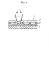
- Fig. 6 is a section of the conventional touch panel.
- Touch panel 8 includes transparent upper substrate 1, such as a film of polyethylene terephthalate, lower substrate 2 made of glass, transparent resin or the like, light-transmitting upper electrode layer 1A formed on a bottom of upper substrate 1, and light-transmitting lower electrode layer 2A formed on a top of lower substrate 2.
- Electrode layers 1A, 2A may be made of indium tin oxide (ITO).
- ITO indium tin oxide
- On the top of lower electrode layer 2A plural dot spacers 3 made of epoxy, silicon, or the like is formed by printing, provides upper and lower electrode layers 1A and 2A with an established spacing between the layers to face each other.
- insulating layer 4 and adhesive layer 5 are formed along an outer border of substrate 2, and upper and lower substrates 1 and 2 are put together by adhesive layer 5.
- Lower substrate 2 is bonded with adhesive layer 7 to a top of transparent supporter 6 made of resin or the like.
- upper substrate 1 When a top of upper substrate 1 is pressed with a finger or pen, as shown in Fig. 7, upper substrate 1 bends, upper electrode layer 1A contacts with lower electrode layer 2A of lower substrate 2. Consequently, upper electrode layer 1A is electrically connected to lower electrode layer 2A.
- elastic restoring force of upper substrate 1 makes panel 8 return to that illustrated by Fig. 6.
- touch panel 8 is installed at a bottom of opening 10A in case 10 of the electronic device, and is mounted to case 10 with holder 12 together with display element 11 (e.g., LCD) disposed below panel 8.
- display element 11 e.g., LCD
- Trough transparent touch panel 8 the characters, the marks, or the patterns displayed on display element 11 are visually identified and selected through pressing upper substrate 1 over element 11.
- the pressing makes touch panel 8 electrically connected and disconnected. In this way, for example, the electronic device switches among functions, or display element 11 switches among displays.
- conventional touch panel 8 mounted to case 10 of the electronic device has a top surface (operating surface) of upper substrate 1 positioned back to a surface of case 10. Therefore, as shown in Fig. 8, the finger or pen touches the surface of case 10 about an outer region of opening 10A when an outer border of upper substrate 1 is pressed for operation. Particularly for this case, a user hardly operate the panel and thus results in improper operation.
- a touch panel and an electronic device using the panel have reliable operability.
- the touch panel includes a light-transmitting upper substrate, a light-transmitting lower substrate spaced from and opposed to the upper substrate, a light-transmitting upper electrode layer on a surface of the upper substrate that faces the lower substrate, and a light-transmitting lower electrode layer provided on a surface of the lower substrate that faces the upper substrate.
- Respective center portion of the upper and lower substrates protrudes in a direction from the lower substrate to the upper substrate like a dome.
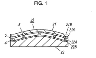
- Fig. 1 is a section of a touch panel in accordance with the embodiment of the present invention.
- Touch panel 25 includes transparent upper substrate 21, such as a film of polyethylene terephthalate or the like, massive, transparent lower substrate 22 that has a flat bottom and is made of polycarbonate, acrylic resin, norbornene resin or the like, light-transmitting upper electrode layer 21A formed on a bottom of upper substrate 21, and light-transmitting lower electrode layer 22A formed on a top of lower substrate 22.
- Electrode layers 21A and 22A may be made of indium tin oxide (ITO). Respective center portions of upper and lower substrates 21 and 22 protrude upward in a shape of a substantially hemispheric dome.
- ITO indium tin oxide
- plural dot spacers 3 made of epoxy, silicon or the like is formed by printing, and provides upper and lower electrode layers 21A and 22A with an established spacing between the layers to face each other.
- Flat portions 21B and 22B are provided at respective outer borders of upper and lower substrates 21 and 22.
- Insulating layer 4, and adhesive layer 5 are formed along and over an outer border of flat part 22B.
- Flat portion 21B is coupled to adhesive layer 5, and thus upper and lower substrates 21 and 22 are put together.
- upper substrate 21 When a top surface of upper substrate 21 is pressed by a finger or pen, upper substrate 21 bends, and upper electrode layer 21A contacts with lower electrode layer 22A of lower substrate 22. Consequently, upper electrode layer 21A is electrically connected to lower electrode layer 22A. Similarly to the prior art, elastic restoring force of upper substrate 21 returns to its original form when pressing force is released.
- touch panel 25 is installed at a bottom side of opening 10A in case 10 of an electronic device to be mounted to case 10 with holder 12 together with display element 11 (e.g., LCD) disposed below panel 25.
- display element 11 e.g., LCD
- the center portion of panel 25 is shaped domelike, and thus upper substrate 21 functioning as an operating side protrudes upward through opening 10A. This allows not only the center portion but also the outer border of panel 25 to be pressed easily, and this prevents the electronic device to be operated incorrectly.
- Trough transparent touch panel 25,, characters, marks, patterns or the like displayed on display element 11 are visually identified and selected though pressing upper substrate 21 over the panel 25.
- the pressing makes touch panel 25 electrically connected and disconnected. In this way, for example, the electronic device switches among functions, or display element 11 switches among displays. Since lower substrate 22 is massive, panel 25 can be mounted directly to case 10 without a supporter.
- touch panel 25 of the embodiment respective center portions of upper and lower substrates 21 and 22 facing with the established spacing protrude upward in a dome shape.
- Touch panel 25 upon being mounted to a bottom of case 10 of the electronic device, has its center portion protrude upward through opening 10A of case 10. This prevents the panel from improper operation, and satisfactory operability is obtained.
- Flat portions 21B and 22B provided at respective outer borders of upper and lower substrates 21 and 22 makes the upper and lower substrates put together easily, and thus the touch panel can be easily held and fixed to case 10 of the electronic device and display element 11.
- display sheet 26 having display marks may be affixed to the outer border of the top surface of upper substrate 21 or the outer border of the bottom surface of lower substrate 22 which does-not cover the screen of display element 11 disposed below.
- Sheet 26 allows switching among functions other than the functions displayed on display element 11, thus widening its functions.
- the display marks may be printed on the substrate instead of the sheet.
- respective dome-like portions of upper and lower substrates 21 and 22 are substantially hemispheric, as illustrated by Fig. 4A.
- the present invention is not limited to this, and the same advantages can be obtained even if the dome-like portion is substantially elliptical as illustrated by Fig. 4B or substantially quadrangular as illustrated by Fig. 4C according to the shape of opening 10A of the device.
- Lower substrate 22 upon being sheet-like or having different thicknesses between the center portion and the outer border, exhibits various lens effects.
- the center portion of the operating side of touch panel 25 protrudes upward relative to a top of case 10.
- the present invention is not limited to this, and the operating side may be positioned slightly back to the top of case 10 with a low dome-like shape when panel 25 is used in a portable device.
- the present invention provides a touch panel and an electronic device using the panel.
- the touch panel has satisfactory operability and is less likely to cause improper operation.
Landscapes
- Engineering & Computer Science (AREA)
- General Engineering & Computer Science (AREA)
- Theoretical Computer Science (AREA)
- Human Computer Interaction (AREA)
- Physics & Mathematics (AREA)
- General Physics & Mathematics (AREA)
- Position Input By Displaying (AREA)
- Push-Button Switches (AREA)
Abstract
Description
Claims (6)
- A touch panel comprising:wherein respective center portions of said first and second substrates protrude in a direction from said second substrate to said first substrate like a dome.a first light-transmitting substrate;a second light-transmitting substrate facing said first substrate with a space;a first light-transmitting electrode layer on a first surface of said first substrate, said first surface of said first substrate facing said second substrate; anda second light-transmitting electrode layer on a first surface of said second substrate, said first surface of said second substrate facing said first substrate,
- The touch panel of claim 1, wherein said center portion of said second substrate is thicker than an outer border of said second substrate.
- The touch panel of claim 1, wherein at least one of said first and second substrates includes a flat portion at an outer border thereof.
- The touch panel of claim 1, further comprising:a display sheet affixed to one of a second surface of said first substrate opposite to said first surface of said first substrate and a second surface of said second substrate opposite to said first surface of said second substrate.
- The touch panel of claim 1, further comprising:a display mark on one of a second surface of said first substrate opposite to said first surface of said first substrate and a second surface of said second substrate opposite to said first surface of said second substrate.
- A device comprising:said touch panel of claim 1;a case having an opening to which said first substrate of said touch panel is engaged; anda display element disposed over said second substrate of said touch panel opposite to said first substrate.
Applications Claiming Priority (3)
| Application Number | Priority Date | Filing Date | Title |
|---|---|---|---|
| JP2000400455A JP2002202855A (en) | 2000-12-28 | 2000-12-28 | Touch panel and electronic device using the same |
| JP2000400455 | 2000-12-28 | ||
| PCT/JP2001/011496 WO2002054218A1 (en) | 2000-12-28 | 2001-12-26 | Touch panel and electronic equipment using the touch panel |
Publications (2)
| Publication Number | Publication Date |
|---|---|
| EP1347364A1 true EP1347364A1 (en) | 2003-09-24 |
| EP1347364A4 EP1347364A4 (en) | 2010-01-20 |
Family
ID=18865046
Family Applications (1)
| Application Number | Title | Priority Date | Filing Date |
|---|---|---|---|
| EP01272884A Withdrawn EP1347364A4 (en) | 2000-12-28 | 2001-12-26 | TOUCH SCREEN AND ELECTRONIC EQUIPMENT OPERATING WITH THIS TOUCH SCREEN |
Country Status (5)
| Country | Link |
|---|---|
| US (1) | US7298366B2 (en) |
| EP (1) | EP1347364A4 (en) |
| JP (1) | JP2002202855A (en) |
| CN (1) | CN1207654C (en) |
| WO (1) | WO2002054218A1 (en) |
Families Citing this family (51)
| Publication number | Priority date | Publication date | Assignee | Title |
|---|---|---|---|---|
| US7312785B2 (en) | 2001-10-22 | 2007-12-25 | Apple Inc. | Method and apparatus for accelerated scrolling |
| US7333092B2 (en) | 2002-02-25 | 2008-02-19 | Apple Computer, Inc. | Touch pad for handheld device |
| JP2004005309A (en) * | 2002-06-03 | 2004-01-08 | Matsushita Electric Ind Co Ltd | Content distribution system and related method or recording medium or program |
| US7499040B2 (en) | 2003-08-18 | 2009-03-03 | Apple Inc. | Movable touch pad with added functionality |
| US20070152977A1 (en) | 2005-12-30 | 2007-07-05 | Apple Computer, Inc. | Illuminated touchpad |
| JP2005100333A (en) * | 2003-09-04 | 2005-04-14 | Alps Electric Co Ltd | Coordinate input device, and liquid crystal display device and electronic apparatus comprising the same |
| US7495659B2 (en) | 2003-11-25 | 2009-02-24 | Apple Inc. | Touch pad for handheld device |
| US8059099B2 (en) | 2006-06-02 | 2011-11-15 | Apple Inc. | Techniques for interactive input to portable electronic devices |
| JP4539241B2 (en) * | 2004-09-02 | 2010-09-08 | パナソニック株式会社 | Touch panel and manufacturing method thereof |
| TW200620251A (en) * | 2004-12-13 | 2006-06-16 | Mitac Technology Corp | Digital audio and video reproducing device |
| JP2006215738A (en) * | 2005-02-02 | 2006-08-17 | Sony Corp | Vibration transmission structure, input device with tactile function, and electronic device |
| JP4545034B2 (en) * | 2005-03-31 | 2010-09-15 | 富士通コンポーネント株式会社 | Touch panel manufacturing method and touch panel |
| US20070152983A1 (en) | 2005-12-30 | 2007-07-05 | Apple Computer, Inc. | Touch pad with symbols based on mode |
| US7791595B2 (en) * | 2006-06-20 | 2010-09-07 | Lutron Electronics Co., Inc. | Touch screen assembly for a lighting control |
| US7608948B2 (en) * | 2006-06-20 | 2009-10-27 | Lutron Electronics Co., Inc. | Touch screen with sensory feedback |
| US8022935B2 (en) | 2006-07-06 | 2011-09-20 | Apple Inc. | Capacitance sensing electrode with integrated I/O mechanism |
| US8743060B2 (en) | 2006-07-06 | 2014-06-03 | Apple Inc. | Mutual capacitance touch sensing device |
| US9360967B2 (en) | 2006-07-06 | 2016-06-07 | Apple Inc. | Mutual capacitance touch sensing device |
| US7795553B2 (en) * | 2006-09-11 | 2010-09-14 | Apple Inc. | Hybrid button |
| US8274479B2 (en) | 2006-10-11 | 2012-09-25 | Apple Inc. | Gimballed scroll wheel |
| US8482530B2 (en) | 2006-11-13 | 2013-07-09 | Apple Inc. | Method of capacitively sensing finger position |
| CN101192258B (en) * | 2006-11-20 | 2012-03-07 | 鸿富锦精密工业(深圳)有限公司 | Electronic device and method for opening same |
| US8683378B2 (en) | 2007-09-04 | 2014-03-25 | Apple Inc. | Scrolling techniques for user interfaces |
| WO2009032898A2 (en) | 2007-09-04 | 2009-03-12 | Apple Inc. | Compact input device |
| US8416198B2 (en) | 2007-12-03 | 2013-04-09 | Apple Inc. | Multi-dimensional scroll wheel |
| US8125461B2 (en) | 2008-01-11 | 2012-02-28 | Apple Inc. | Dynamic input graphic display |
| US8820133B2 (en) | 2008-02-01 | 2014-09-02 | Apple Inc. | Co-extruded materials and methods |
| US9454256B2 (en) | 2008-03-14 | 2016-09-27 | Apple Inc. | Sensor configurations of an input device that are switchable based on mode |
| US20090309826A1 (en) | 2008-06-17 | 2009-12-17 | Searete Llc, A Limited Liability Corporation Of The State Of Delaware | Systems and devices |
| US20090312854A1 (en) * | 2008-06-17 | 2009-12-17 | Searete Llc, A Limited Liability Corporation Of The State Of Delaware | Methods and systems for transmitting information associated with the coordinated use of two or more user responsive projectors |
| US8944608B2 (en) | 2008-06-17 | 2015-02-03 | The Invention Science Fund I, Llc | Systems and methods associated with projecting in response to conformation |
| US8955984B2 (en) | 2008-06-17 | 2015-02-17 | The Invention Science Fund I, Llc | Projection associated methods and systems |
| US8936367B2 (en) | 2008-06-17 | 2015-01-20 | The Invention Science Fund I, Llc | Systems and methods associated with projecting in response to conformation |
| US20110157065A1 (en) * | 2008-09-18 | 2011-06-30 | Sharp Kabushiki Kaisha | Touch panel, display device, and electronic device |
| US8816967B2 (en) | 2008-09-25 | 2014-08-26 | Apple Inc. | Capacitive sensor having electrodes arranged on the substrate and the flex circuit |
| US8395590B2 (en) | 2008-12-17 | 2013-03-12 | Apple Inc. | Integrated contact switch and touch sensor elements |
| US9354751B2 (en) | 2009-05-15 | 2016-05-31 | Apple Inc. | Input device with optimized capacitive sensing |
| US8872771B2 (en) | 2009-07-07 | 2014-10-28 | Apple Inc. | Touch sensing device having conductive nodes |
| JP5065431B2 (en) * | 2010-03-31 | 2012-10-31 | キヤノン株式会社 | Image reading apparatus and operation panel |
| US20110261002A1 (en) * | 2010-04-27 | 2011-10-27 | Microsoft Corporation | Displaying images on solid surfaces |
| JP5581904B2 (en) * | 2010-08-31 | 2014-09-03 | 日本精機株式会社 | Input device |
| TWI459274B (en) * | 2011-11-28 | 2014-11-01 | Shih Hua Technology Ltd | Touch panel model and method for making the same |
| JP5839470B2 (en) * | 2012-01-31 | 2016-01-06 | 富士通コンポーネント株式会社 | Pointing device and manufacturing method thereof |
| JP6199541B2 (en) | 2012-04-19 | 2017-09-20 | 富士通コンポーネント株式会社 | Touch input device |
| JP5999340B2 (en) * | 2012-10-05 | 2016-09-28 | 日本電気硝子株式会社 | Glass film laminate for touch panel, touch panel, and method for producing glass film laminate for touch panel |
| JP5672338B2 (en) * | 2013-06-04 | 2015-02-18 | Smk株式会社 | Touch panel and method for manufacturing touch panel |
| JP6348302B2 (en) * | 2014-02-28 | 2018-06-27 | 株式会社デンソーテン | Image display device |
| US9811707B2 (en) | 2014-06-04 | 2017-11-07 | Lenovo (Singapore) Pte. Ltd. | Fingerprint reader on a portion of a device for changing the configuration of the device |
| US20170108959A1 (en) * | 2015-10-15 | 2017-04-20 | Richard Keith McMillan | Two piece lens assembly |
| DE102015120606A1 (en) * | 2015-11-27 | 2017-06-01 | Valeo Schalter Und Sensoren Gmbh | Curved detection device for a motor vehicle, operating arrangement and motor vehicle |
| KR20170073224A (en) * | 2015-12-18 | 2017-06-28 | 주식회사 트레이스 | Touch screen using 3d dome type touch pattern |
Family Cites Families (20)
| Publication number | Priority date | Publication date | Assignee | Title |
|---|---|---|---|---|
| GB1562264A (en) * | 1976-11-22 | 1980-03-12 | Control Data Corp | Electric switch matrix |
| JPS59104764A (en) * | 1982-12-03 | 1984-06-16 | Canon Inc | LCD display keyboard |
| JPH01102625A (en) * | 1987-10-15 | 1989-04-20 | Canon Inc | Information input/output device |
| JPH04309163A (en) * | 1991-04-08 | 1992-10-30 | Matsushita Electric Ind Co Ltd | Device for enlarging control key of terminal |
| JPH05197493A (en) * | 1991-06-14 | 1993-08-06 | Akira Ishii | Dome-shaped touch pannel and method for forming transparent conductive material-coated transparent plastic film dome |
| US5274198A (en) * | 1991-12-26 | 1993-12-28 | Cal Comp Inc. | Printed conductive ink electrostatic shield for electromagnetic digitizers |
| CA2161634C (en) * | 1993-04-28 | 2004-04-27 | Kenichirou Ikura | Transparent touch panel |
| JP3277645B2 (en) * | 1993-11-01 | 2002-04-22 | 株式会社日立製作所 | Pen input type information processing device |
| US5613137A (en) * | 1994-03-18 | 1997-03-18 | International Business Machines Corporation | Computer system with touchpad support in operating system |
| JPH07322012A (en) * | 1994-05-27 | 1995-12-08 | Fuji Xerox Co Ltd | Picture input/output device |
| JPH08328741A (en) * | 1995-06-01 | 1996-12-13 | Digital:Kk | Liquid crystal display device provided with touch panel |
| US5736688A (en) * | 1995-08-02 | 1998-04-07 | The Graphics Technology Company, Inc. | Curvilinear linearization device for touch systems |
| JPH09305296A (en) * | 1996-05-17 | 1997-11-28 | Fujitsu Takamizawa Component Kk | Coordinate input device |
| JPH10257148A (en) * | 1997-03-10 | 1998-09-25 | Sanwa Insatsu:Kk | Display device for portable telephone set |
| JPH11161428A (en) * | 1997-05-16 | 1999-06-18 | Dmc:Kk | Touch panel sensor device |
| JPH11184631A (en) * | 1997-12-22 | 1999-07-09 | Casio Comput Co Ltd | Curved touch panel |
| JP4435890B2 (en) * | 1999-01-12 | 2010-03-24 | 日本写真印刷株式会社 | Touch panel |
| JP3946371B2 (en) * | 1999-01-12 | 2007-07-18 | 日本写真印刷株式会社 | Touch panel |
| JP2001154592A (en) * | 1999-09-13 | 2001-06-08 | Minolta Co Ltd | Display device |
| TW579019U (en) * | 2001-06-13 | 2004-03-01 | Eturbotouch Technology Inc | Flexible current type touch film |
-
2000
- 2000-12-28 JP JP2000400455A patent/JP2002202855A/en not_active Withdrawn
-
2001
- 2001-12-26 WO PCT/JP2001/011496 patent/WO2002054218A1/en not_active Ceased
- 2001-12-26 CN CNB018054048A patent/CN1207654C/en not_active Expired - Fee Related
- 2001-12-26 EP EP01272884A patent/EP1347364A4/en not_active Withdrawn
- 2001-12-26 US US10/204,705 patent/US7298366B2/en not_active Expired - Fee Related
Also Published As
| Publication number | Publication date |
|---|---|
| JP2002202855A (en) | 2002-07-19 |
| WO2002054218A1 (en) | 2002-07-11 |
| CN1404585A (en) | 2003-03-19 |
| EP1347364A4 (en) | 2010-01-20 |
| CN1207654C (en) | 2005-06-22 |
| US20030122792A1 (en) | 2003-07-03 |
| US7298366B2 (en) | 2007-11-20 |
Similar Documents
| Publication | Publication Date | Title |
|---|---|---|
| US7298366B2 (en) | Touch panel and electronic equipment using the same | |
| US8403576B2 (en) | Keyboard for hand held computing device | |
| TWI409842B (en) | Sheet switch module | |
| CN101488409A (en) | Movable contact body and switch using same | |
| EP3288055B1 (en) | Keyswitch assembly and manufacturing method thereof | |
| JP3884906B2 (en) | Liquid crystal display | |
| JP2003197056A (en) | Display device with input function and electronic device using the same | |
| US20140152596A1 (en) | Mobile communication device | |
| JPH1139984A (en) | EL illuminated switch | |
| EP2224315B1 (en) | Keypad assembly using optical shutter and light guide panel and portable terminal having the same | |
| KR101534855B1 (en) | Button input device | |
| JP3995410B2 (en) | Liquid crystal display | |
| JP2578772Y2 (en) | Key top support structure and key switch | |
| CN100362460C (en) | touch screen | |
| US20090065335A1 (en) | Multi-functional keypad module for a mobile phone | |
| KR100822187B1 (en) | Touch panel and flat panel display device using same | |
| JP3395580B2 (en) | Input/Output Devices | |
| JP2002131724A (en) | Liquid crystal display | |
| JP2000047820A (en) | Transparent touch panel and display device using the same | |
| KR20040012294A (en) | Touch panel device with fingerprint recognition sensor | |
| JP4215940B2 (en) | Self-illuminating sheet material | |
| JP2004102813A (en) | Electronic device | |
| US10234896B2 (en) | Display assembly and interface for a communication device | |
| JP2014093010A (en) | Touch panel | |
| JP2005339220A (en) | Display sheet and input device using the same |
Legal Events
| Date | Code | Title | Description |
|---|---|---|---|
| PUAI | Public reference made under article 153(3) epc to a published international application that has entered the european phase |
Free format text: ORIGINAL CODE: 0009012 |
|
| 17P | Request for examination filed |
Effective date: 20020828 |
|
| AK | Designated contracting states |
Kind code of ref document: A1 Designated state(s): AT BE CH CY DE DK ES FI FR GB GR IE IT LI LU MC NL PT SE TR |
|
| RBV | Designated contracting states (corrected) |
Designated state(s): DE FI FR GB |
|
| RAP1 | Party data changed (applicant data changed or rights of an application transferred) |
Owner name: PANASONIC CORPORATION |
|
| A4 | Supplementary search report drawn up and despatched |
Effective date: 20091217 |
|
| RIC1 | Information provided on ipc code assigned before grant |
Ipc: G02F 1/133 20060101ALI20091211BHEP Ipc: G06F 3/033 20060101AFI20020716BHEP |
|
| STAA | Information on the status of an ep patent application or granted ep patent |
Free format text: STATUS: THE APPLICATION IS DEEMED TO BE WITHDRAWN |
|
| 18D | Application deemed to be withdrawn |
Effective date: 20100316 |