EP1347082A1 - Method and apparatus for growing single crystal - Google Patents
Method and apparatus for growing single crystal Download PDFInfo
- Publication number
- EP1347082A1 EP1347082A1 EP01272881A EP01272881A EP1347082A1 EP 1347082 A1 EP1347082 A1 EP 1347082A1 EP 01272881 A EP01272881 A EP 01272881A EP 01272881 A EP01272881 A EP 01272881A EP 1347082 A1 EP1347082 A1 EP 1347082A1
- Authority
- EP
- European Patent Office
- Prior art keywords
- single crystal
- cooling
- growing
- cooling cylinder
- copper
- Prior art date
- Legal status (The legal status is an assumption and is not a legal conclusion. Google has not performed a legal analysis and makes no representation as to the accuracy of the status listed.)
- Ceased
Links
- 239000013078 crystal Substances 0.000 title claims abstract description 231
- 238000000034 method Methods 0.000 title claims abstract description 32
- 238000001816 cooling Methods 0.000 claims abstract description 183
- RYGMFSIKBFXOCR-UHFFFAOYSA-N Copper Chemical compound [Cu] RYGMFSIKBFXOCR-UHFFFAOYSA-N 0.000 claims abstract description 85
- 239000010949 copper Substances 0.000 claims abstract description 85
- 229910052802 copper Inorganic materials 0.000 claims abstract description 84
- 239000002826 coolant Substances 0.000 claims abstract description 49
- 229910052751 metal Inorganic materials 0.000 claims abstract description 13
- 239000002184 metal Substances 0.000 claims abstract description 13
- 239000000155 melt Substances 0.000 claims description 50
- 239000002994 raw material Substances 0.000 claims description 45
- XLYOFNOQVPJJNP-UHFFFAOYSA-N water Substances O XLYOFNOQVPJJNP-UHFFFAOYSA-N 0.000 claims description 14
- 238000010438 heat treatment Methods 0.000 claims description 5
- 239000007787 solid Substances 0.000 claims description 5
- XUIMIQQOPSSXEZ-UHFFFAOYSA-N Silicon Chemical compound [Si] XUIMIQQOPSSXEZ-UHFFFAOYSA-N 0.000 abstract description 39
- 229910052710 silicon Inorganic materials 0.000 abstract description 39
- 239000010703 silicon Substances 0.000 abstract description 39
- 230000000694 effects Effects 0.000 abstract description 26
- 238000002844 melting Methods 0.000 description 13
- 230000008018 melting Effects 0.000 description 13
- 238000002474 experimental method Methods 0.000 description 12
- 239000000463 material Substances 0.000 description 11
- 239000010935 stainless steel Substances 0.000 description 9
- 229910001220 stainless steel Inorganic materials 0.000 description 9
- 239000007789 gas Substances 0.000 description 8
- 238000007711 solidification Methods 0.000 description 8
- 230000008023 solidification Effects 0.000 description 8
- 239000000498 cooling water Substances 0.000 description 7
- 238000006243 chemical reaction Methods 0.000 description 6
- 230000007246 mechanism Effects 0.000 description 6
- BQCADISMDOOEFD-UHFFFAOYSA-N Silver Chemical compound [Ag] BQCADISMDOOEFD-UHFFFAOYSA-N 0.000 description 5
- 230000000052 comparative effect Effects 0.000 description 5
- 238000004519 manufacturing process Methods 0.000 description 5
- 229910052709 silver Inorganic materials 0.000 description 5
- 239000004332 silver Substances 0.000 description 5
- XKRFYHLGVUSROY-UHFFFAOYSA-N Argon Chemical compound [Ar] XKRFYHLGVUSROY-UHFFFAOYSA-N 0.000 description 4
- 229910000577 Silicon-germanium Inorganic materials 0.000 description 4
- 238000011109 contamination Methods 0.000 description 4
- 238000009826 distribution Methods 0.000 description 4
- 239000010453 quartz Substances 0.000 description 4
- VYPSYNLAJGMNEJ-UHFFFAOYSA-N silicon dioxide Inorganic materials O=[Si]=O VYPSYNLAJGMNEJ-UHFFFAOYSA-N 0.000 description 4
- 238000012546 transfer Methods 0.000 description 4
- 238000004804 winding Methods 0.000 description 4
- OKTJSMMVPCPJKN-UHFFFAOYSA-N Carbon Chemical compound [C] OKTJSMMVPCPJKN-UHFFFAOYSA-N 0.000 description 3
- 230000008859 change Effects 0.000 description 3
- 230000003247 decreasing effect Effects 0.000 description 3
- 229910002804 graphite Inorganic materials 0.000 description 3
- 239000010439 graphite Substances 0.000 description 3
- 239000007788 liquid Substances 0.000 description 3
- 238000004088 simulation Methods 0.000 description 3
- 229910001316 Ag alloy Inorganic materials 0.000 description 2
- 229910000881 Cu alloy Inorganic materials 0.000 description 2
- 229910052786 argon Inorganic materials 0.000 description 2
- 230000007547 defect Effects 0.000 description 2
- 238000004880 explosion Methods 0.000 description 2
- 238000007654 immersion Methods 0.000 description 2
- 230000006872 improvement Effects 0.000 description 2
- 239000011261 inert gas Substances 0.000 description 2
- 239000011810 insulating material Substances 0.000 description 2
- 239000003507 refrigerant Substances 0.000 description 2
- 230000008646 thermal stress Effects 0.000 description 2
- 235000012431 wafers Nutrition 0.000 description 2
- 208000019901 Anxiety disease Diseases 0.000 description 1
- NEIHULKJZQTQKJ-UHFFFAOYSA-N [Cu].[Ag] Chemical compound [Cu].[Ag] NEIHULKJZQTQKJ-UHFFFAOYSA-N 0.000 description 1
- 230000002776 aggregation Effects 0.000 description 1
- 238000004220 aggregation Methods 0.000 description 1
- 230000036506 anxiety Effects 0.000 description 1
- QVGXLLKOCUKJST-UHFFFAOYSA-N atomic oxygen Chemical compound [O] QVGXLLKOCUKJST-UHFFFAOYSA-N 0.000 description 1
- 238000009529 body temperature measurement Methods 0.000 description 1
- 150000001875 compounds Chemical class 0.000 description 1
- 238000007796 conventional method Methods 0.000 description 1
- YCKOAAUKSGOOJH-UHFFFAOYSA-N copper silver Chemical compound [Cu].[Ag].[Ag] YCKOAAUKSGOOJH-UHFFFAOYSA-N 0.000 description 1
- 230000007797 corrosion Effects 0.000 description 1
- 238000005260 corrosion Methods 0.000 description 1
- 238000007599 discharging Methods 0.000 description 1
- 239000012530 fluid Substances 0.000 description 1
- -1 for example Chemical compound 0.000 description 1
- 229910001385 heavy metal Inorganic materials 0.000 description 1
- 239000012535 impurity Substances 0.000 description 1
- 230000002401 inhibitory effect Effects 0.000 description 1
- 239000001301 oxygen Substances 0.000 description 1
- 229910052760 oxygen Inorganic materials 0.000 description 1
- 238000001556 precipitation Methods 0.000 description 1
- 230000009257 reactivity Effects 0.000 description 1
- 239000004065 semiconductor Substances 0.000 description 1
- 230000035939 shock Effects 0.000 description 1
- 229910000679 solder Inorganic materials 0.000 description 1
- 238000005476 soldering Methods 0.000 description 1
- 238000003466 welding Methods 0.000 description 1
Images


Classifications
-
- C—CHEMISTRY; METALLURGY
- C30—CRYSTAL GROWTH
- C30B—SINGLE-CRYSTAL GROWTH; UNIDIRECTIONAL SOLIDIFICATION OF EUTECTIC MATERIAL OR UNIDIRECTIONAL DEMIXING OF EUTECTOID MATERIAL; REFINING BY ZONE-MELTING OF MATERIAL; PRODUCTION OF A HOMOGENEOUS POLYCRYSTALLINE MATERIAL WITH DEFINED STRUCTURE; SINGLE CRYSTALS OR HOMOGENEOUS POLYCRYSTALLINE MATERIAL WITH DEFINED STRUCTURE; AFTER-TREATMENT OF SINGLE CRYSTALS OR A HOMOGENEOUS POLYCRYSTALLINE MATERIAL WITH DEFINED STRUCTURE; APPARATUS THEREFOR
- C30B15/00—Single-crystal growth by pulling from a melt, e.g. Czochralski method
-
- C—CHEMISTRY; METALLURGY
- C30—CRYSTAL GROWTH
- C30B—SINGLE-CRYSTAL GROWTH; UNIDIRECTIONAL SOLIDIFICATION OF EUTECTIC MATERIAL OR UNIDIRECTIONAL DEMIXING OF EUTECTOID MATERIAL; REFINING BY ZONE-MELTING OF MATERIAL; PRODUCTION OF A HOMOGENEOUS POLYCRYSTALLINE MATERIAL WITH DEFINED STRUCTURE; SINGLE CRYSTALS OR HOMOGENEOUS POLYCRYSTALLINE MATERIAL WITH DEFINED STRUCTURE; AFTER-TREATMENT OF SINGLE CRYSTALS OR A HOMOGENEOUS POLYCRYSTALLINE MATERIAL WITH DEFINED STRUCTURE; APPARATUS THEREFOR
- C30B15/00—Single-crystal growth by pulling from a melt, e.g. Czochralski method
- C30B15/14—Heating of the melt or the crystallised materials
-
- C—CHEMISTRY; METALLURGY
- C30—CRYSTAL GROWTH
- C30B—SINGLE-CRYSTAL GROWTH; UNIDIRECTIONAL SOLIDIFICATION OF EUTECTIC MATERIAL OR UNIDIRECTIONAL DEMIXING OF EUTECTOID MATERIAL; REFINING BY ZONE-MELTING OF MATERIAL; PRODUCTION OF A HOMOGENEOUS POLYCRYSTALLINE MATERIAL WITH DEFINED STRUCTURE; SINGLE CRYSTALS OR HOMOGENEOUS POLYCRYSTALLINE MATERIAL WITH DEFINED STRUCTURE; AFTER-TREATMENT OF SINGLE CRYSTALS OR A HOMOGENEOUS POLYCRYSTALLINE MATERIAL WITH DEFINED STRUCTURE; APPARATUS THEREFOR
- C30B29/00—Single crystals or homogeneous polycrystalline material with defined structure characterised by the material or by their shape
- C30B29/02—Elements
- C30B29/06—Silicon
-
- Y—GENERAL TAGGING OF NEW TECHNOLOGICAL DEVELOPMENTS; GENERAL TAGGING OF CROSS-SECTIONAL TECHNOLOGIES SPANNING OVER SEVERAL SECTIONS OF THE IPC; TECHNICAL SUBJECTS COVERED BY FORMER USPC CROSS-REFERENCE ART COLLECTIONS [XRACs] AND DIGESTS
- Y10—TECHNICAL SUBJECTS COVERED BY FORMER USPC
- Y10T—TECHNICAL SUBJECTS COVERED BY FORMER US CLASSIFICATION
- Y10T117/00—Single-crystal, oriented-crystal, and epitaxy growth processes; non-coating apparatus therefor
- Y10T117/10—Apparatus
- Y10T117/1024—Apparatus for crystallization from liquid or supercritical state
- Y10T117/1032—Seed pulling
-
- Y—GENERAL TAGGING OF NEW TECHNOLOGICAL DEVELOPMENTS; GENERAL TAGGING OF CROSS-SECTIONAL TECHNOLOGIES SPANNING OVER SEVERAL SECTIONS OF THE IPC; TECHNICAL SUBJECTS COVERED BY FORMER USPC CROSS-REFERENCE ART COLLECTIONS [XRACs] AND DIGESTS
- Y10—TECHNICAL SUBJECTS COVERED BY FORMER USPC
- Y10T—TECHNICAL SUBJECTS COVERED BY FORMER US CLASSIFICATION
- Y10T117/00—Single-crystal, oriented-crystal, and epitaxy growth processes; non-coating apparatus therefor
- Y10T117/10—Apparatus
- Y10T117/1024—Apparatus for crystallization from liquid or supercritical state
- Y10T117/1032—Seed pulling
- Y10T117/1068—Seed pulling including heating or cooling details [e.g., shield configuration]
-
- Y—GENERAL TAGGING OF NEW TECHNOLOGICAL DEVELOPMENTS; GENERAL TAGGING OF CROSS-SECTIONAL TECHNOLOGIES SPANNING OVER SEVERAL SECTIONS OF THE IPC; TECHNICAL SUBJECTS COVERED BY FORMER USPC CROSS-REFERENCE ART COLLECTIONS [XRACs] AND DIGESTS
- Y10—TECHNICAL SUBJECTS COVERED BY FORMER USPC
- Y10T—TECHNICAL SUBJECTS COVERED BY FORMER US CLASSIFICATION
- Y10T117/00—Single-crystal, oriented-crystal, and epitaxy growth processes; non-coating apparatus therefor
- Y10T117/10—Apparatus
- Y10T117/1024—Apparatus for crystallization from liquid or supercritical state
- Y10T117/1032—Seed pulling
- Y10T117/1072—Seed pulling including details of means providing product movement [e.g., shaft guides, servo means]
Definitions
- the present invention relates to a method for growing a single crystal and apparatus for growing a single crystal used for production of single crystals such as silicon single crystals by the Czochralski method (also referred to as the "CZ method” or “pulling method” hereinafter).
- An apparatus for growing a single crystal used for producing a silicon single crystal by the CZ method generally comprises a crucible containing a raw material melt, which can be moved upwardly and downwardly, and a heater disposed so as to surround the crucible, both of which are provided in a main chamber for growing a single crystal, and a pulling chamber for containing and taking out a grown single crystal is continuously provided above the main chamber.
- the seed crystal attached to a seed holder is immersed into the raw material melt, and then the seed crystal is pulled upwardly with rotation in a desired direction by carefully winding up a wire by means of a pulling mechanism to grow a single crystal ingot at the end of the seed crystal.
- the crystal in an early stage of the growth is once made thin to a small diameter of about 3 to 5 mm, and then the diameter is increased after the dislocation are eliminated so as to grow a single crystal ingot of desired quality.
- the pulling rate for a portion having a constant diameter of the single crystal ingot is usually extremely slow, i.e., about 0.5 to 1 mm/min, and if it is pulled fast by constraint, there are arisen various problems.
- the growing single crystal is deformed and thus a cylindrical product having a constant diameter can no longer be obtained, slip dislocations are generated in the single crystal ingot, the crystal is detached from the melt and thus it cannot be a product and so forth. Therefore, increase of the crystal growth rate is limited.
- the pulling rate i.e., the single crystal growth rate
- the heat quantity incorporated into the crystal consists of inflow heat quantity from the melt and the heater and solidification latent heat generated when the melt crystallizes.
- outflow heat quantity emitted out of the crystal from the crystal surface and through the seed crystal should be equal to the sum of the inflow heat quantity and the solidification latent heat.
- the solidification latent heat depends on the volume of the crystal growing per unit time. Therefore, in order to increase the crystal growth rate, it is necessary to compensate increase of solidification latent heat provided by increase of the crystal growth rate by reducing the inflow heat quantity or increasing the outflow heat quantity.
- a gas flow guide cooling cylinder having a double structure consisting of an outer cooling cylinder composed of metal and an inner cooling cylinder composed of graphite or the like is provided from the bottom portion of the pulling chamber to the inside of the main chamber so as to concentrically surround a single crystal ingot under pulling and thereby heat generated in the inner cooling cylinder is transferred to the outside by the outer cooling cylinder, so that temperature increase of the inner cooling cylinder should be suppressed and cooling efficiency of the crystal should be improved.
- Apparatuses utilizing a cooling medium such as water in order to more efficiently cool a growing single crystal are also disclosed.
- a cooling duct for circulating a liquid refrigerant is provided in a main chamber and a cooling member composed of a . material having high heat conductivity such as silver is provided below the duct so as to rapidly transfer heat emitted from crystal surface to the outside and thereby attain effective cooling of the crystal.
- fluid such as water generally used as the cooling medium become close to the melt surface heated to a high temperature exceeding 1000°C, it may be a cause of phreatic explosion and thus dangerous. Therefore, in this apparatus, safety is secured by separating the cooling duct from the melt surface.
- the present invention was accomplished in view of the aforementioned problem, and an object of the present invention is to provide a method for growing a single crystal and apparatus for growing a single crystal that can exert cooling effect on a growing single crystal to the maximum extent so as to realize higher crystal growth rate, even when a silicon single crystal having a diameter of 300 mm or more is grown.
- the method for growing a single crystal of the present invention is a method for growing a single crystal by the Czochralski method, wherein a single crystal is grown with forced cooling of neighborhood of a crystal growth interface by disposing a cooling cylinder formed of copper or a metal having a heat conductivity larger than that of copper at least in the vicinity of the crystal. growth interface so as to surround the single crystal under pulling and circulating a cooling medium in the cooling cylinder.
- a cooling cylinder formed of copper or a metal having a heat conductivity larger than that of copper, which has high heat resistance and high heat conductivity, and forcibly cooled by the circulation of the cooling medium in the neighborhood immediately above the liquid-solid growing interface of the single crystal near the raw material melt to forcibly cool neighborhood of the crystal growth interface, the single crystal pulled from the raw material melt and having an extremely high temperature is shielded from the radiant heat from a heater and heat from the single crystal is rapidly absorbed. Therefore, the growth rate of the crystal can be markedly accelerated.
- the single crystal is preferably pulled with adjusting a position of the melt surface so that Distance A (mm) between a lower end of the cooling cylinder and the raw material melt surface and Distance B (mm) between a lower end of the cooling medium circulating in the cooling cylinder and the raw material melt surface should satisfy a relationship of 100 ⁇ B ⁇ A ⁇ 5. Further, it is more preferred that Distance A and Distance B should satisfy a relationship of B - A ⁇ 50.
- the cooling cylinder and the cooling medium can be brought close to the melt surface without contact with the melt, and thus the growing single crystal can be cooled efficiently and safely. Therefore, a single crystal of large size having a diameter exceeding 300 mm can be grown at a high speed, and thus the productivity and yield can be improved.
- the apparatus for growing a single crystal of the present invention is an apparatus for growing a single crystal based on the Czochralski method comprising at least a main chamber enclosing a crucible for containing a raw material melt and a heater for heating the raw material melt, a pulling chamber continuously provided above the main chamber, into which a grown single crystal is pulled and stored, and a cooling cylinder surrounding the single crystal under pulling, wherein at least the cooling cylinder is composed of copper or a metal having a heat conductivity larger than that of copper, is forcibly cooled by circulation of a cooling medium, and extends from an upper portion of the main chamber toward a raw material melt surface so as to cool neighborhood of a crystal growth interface.
- the growing single crystal can be forcibly cooled efficiently and rapidly in the vicinity of the crystal growth interface. Therefore, the growth rate of the crystal can be increased, and the productivity and yield of the single crystal production can be improved.
- the material of the cooling cylinder copper or a metal having a heat conductivity larger than that of copper, for example, silver, copper-silver alloy etc., is extremely excellent in heat resistance and shows extremely high heat conductivity, the radiant heat from the melt and heater is effectively shielded, and surface temperature of the cooling cylinder formed of copper or the like becomes low if it is forcibly cooled with a cooling medium. Therefore, it is suitable for cooling a single crystal ingot at an extremely high temperature immediately after the pulling from the melt surface.
- the cooling cylinder may have a hollow structure for circulation of the cooling medium, or it may consist of a solid cooling cylinder wound with a cooling pipe for circulation of the cooling medium. Further, as the cooling medium, water is preferably used.
- a cooling cylinder structure of so-called jacket structure provided with a box-shaped cylindrical hollow or so-called coil structure in which the cylinder is formed with a single solid plate and a cooling pipe is wound around it, and water available at a low cost and showing high heat conductivity and no corrosive property is used as the cooling medium circulating in the cooling cylinder of hollow structure or the cooling pipe, the radiant heat from the heater and the melt surface and the outflow heat emitted from the growing crystal can be absorbed, and thus the growing single crystal can be efficiently cooled.
- the.cooling cylinder and so forth are preferably disposed so that Distance A (mm) between the lower end of the cooling cylinder and the raw material melt surface and Distance B (mm) between a lower end of the cooling medium circulating in the cooling cylinder and the raw material melt surface should satisfy the relationship of 100 ⁇ B ⁇ A ⁇ 5 during pulling of the crystal. Further, it is more preferred that Distance A and Distance B should satisfy the relationship of B - A ⁇ 50.
- the apparatus can be an apparatus that can grow a single crystal of large size having a diameter exceeding 300 mm with extremely high productivity due to higher growth rate.
- the method for growing a single crystal and apparatus for growing a single crystal of the present invention are characterized in that a single crystal is grown with forced cooling of neighborhood of a crystal growth interface by disposing a cooling cylinder formed of copper or a metal having a heat conductivity larger than that of copper at least in the vicinity of the crystal growth interface so as to surround a growing single crystal and circulating a cooling medium in the cooling cylinder. Because of this characteristic, the cooling effect for the crystal can be exerted to the maximum extent, and thus the pulling rate can be increased to drastically increase the productivity of the crystal.
- the cooling cylinder is free from a fear of corrosion or breakage even when it is brought into contact with the melt at an extremely high temperature and thus protected. Therefore, a further higher level of safety is secured.
- the inventors of the present invention carried out the experiments described hereinafter in order to solve the problem concerning safety and find out means drastically improving the cooling effect, and obtained a novel finding that if a material having high heat conductivity such as copper is used for a cooling pipe for circulating the cooling medium, the cooling pipe can retain the cooling medium without breakage or melting thereof even if the cooling pipe is brought into contact with the raw material melt at a high temperature, that is, it becomes possible to make the cooling medium and the raw material melt closer extremely safely. Thus, they accomplished the present invention.
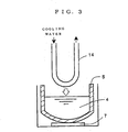
- a U-shaped copper pipe 14 (outer diameter: 8 mm, wall thickness: 0.8 mm) and a small size quartz crucible 5 (inner diameter: 48 mm, provided with a heater at bottom) as shown in Fig. 3 were prepared.
- the surface temperature For melting of the copper pipe, the surface temperature must reach 1083°C, which is the melting point of copper. However, considering that . the temperature of the internal surface should be 100°C or lower (25-28°C) because of the water cooling of the internal surface, there must be a temperature difference of about 1000°C in the wall thickness of 0.8 mm. Since the temperature gradient in this case should be 1.25 x 10 6 K/ m , there must be a heat flow rate of 5.0 x 10 8 K/m 2 , which is obtained by multiplying the temperature gradient by the heat conductivity of copper at 0°C, 401 W/mK.
- stainless steel e.g., SUS316L (JIS Standard)
- SUS316L JIS Standard
- the surface temperature is likely to increase when it is brought into contact with the raw material melt.
- welding portions must be used at positions applied with thermal stress due to the structure of the cooling cylinder, reliability becomes low.
- copper also has the characteristic of ductility, it is unlikely to generate cracks even if thermal stress is applied, and therefore it is considered a material suitable for the cooling cylinder.
- cooling cylinder by a method of winding a copper pipe around a copper plate in a cylindrical shape and fixing it by silver soldering. Since the copper surface has a temperature of 100°C or lower, contamination with copper from the surface is improbable.
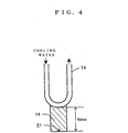
- a copper plate 15 (length: 50 mm, width: 20 mm, thickness: 2 mm) was welded at an end of a water-cooled copper pipe 14 the same as that of the experimental example 1 by using silver solder as shown in Fig. 4, and an experiment was performed in which the copper plate portion was immersed into a silicon melt.
- a thermocouple 21 was provided at the lower end of the copper plate 15 so as to enable temperature measurement.
- the flow rate of cooling water was set to be 6.6 L/min, and the temperature of the silicon melt was adjusted to 1520°C, which was higher than the melting point by 100°C. In this state, the temperature of the lower end of the copper plate 15 located about 4 cm above the melt surface became 465°C.
- the contacting portion was heated slowly to redness and melted soon. Then, the copper plate 15 was once separated from the melt, the temperature of the melt was lowered by 50°C to a temperature higher than the melting point by 50°C (1470°C), and then the copper plate 15 was descended again and brought into contact with the silicon melt 4. At this time, silicon of the contacting position was solidified.
- the copper plate was changed to a stainless steel plate (SUS316L), and the temperature of the lower end of the stainless steel plate located 4 cm above of the surface of the silicon melt at 1470°C was measured. The temperature was 905°C.
- the stainless steel plate was descended and brought into contact with the silicon melt under the same conditions, the contacting portion emitted a white light and was instantly melted.
- the contacting portion again emitted a white light and was melted instantly. The same phenomenon was observed even when the length of the stainless steel plate was shortened by about 30 mm and the end became closer to the water-cooled copper pipe.
- the present invention will be specifically explained by exemplifying growth of silicon single crystals with reference to the appended drawings.
- the present invention is not limited only to growth of these silicon single crystals.
- the apparatus of the present invention can be also used for growth of other single crystals such as those of compound semiconductors.
- Fig. 1 is a sectional view showing a schematic structure of an exemplary apparatus for growing a single crystal according to the present invention.
- a crucible 5 for containing a raw material such as polycrystal silocon melt 4 a heater 7 for heating and melting the polycrystal silicon raw material and so forth are contained in a main chamber 1, and on top of a pulling chamber 2 continuously provided on the main chamber 1, a pulling mechanism (not shown) for pulling a grown single crystal is provided. .
- a pulling wire 16 is reeled out, and a seed holder 18 for attaching a seed crystal 17 is connected at the end of the wire.
- the seed crystal 17 attached at the end of the seed holder 18 is immersed into the raw material melt 4, and a single crystal ingot 3 is formed below the seed crystal 17 by winding the pulling wire 16 by the pulling mechanism.
- the aforementioned crucible is constituted by an inside quartz crucible 5 for directly containing the raw material melt 4 and an outside graphite crucible 6 for supporting the quartz crucible 5.
- the crucibles 5 and 6 are supported by a crucible rotating shaft 19 that can be rotated and moved upwardly and downwardly by a rotation drive mechanism (not shown) provided at a lower portion of the apparatus 20 for growing a single crystal.
- the crucibles are rotated in a direction reverse to the rotating direction of the crystal and moved upwardly for a height of melt surface lowered by. decrease of the melt according to the pulling of a single crystal ingot 3, so that the height of the melt surface should be maintained constant, in order to prevent change of crystal quality with respect to change of the melt surface in the apparatus for growing a single crystal.
- the heater 7 is disposed so that it should surround the crucibles 5 and 6, and a heat insulating member 8 for preventing the heat from the heater 7 from directly radiating the main chamber 1 is provided outside the heater 7 so that it should surround the heater.
- an inert gas such as argon gas is introduced into the chambers 1 and 2 from a gas inlet 10 provided at an upper part of the pulling chamber 2 with the purpose of discharging reaction gases generated in the furnace out of the furnace etc., passed through a space above the single crystal ingot 3 under pulling and the melt 4 to circulate inside the chambers 1 and 2, and then discharged from a gas outlet 9.
- the main chamber 1 and the pulling chamber 2 are formed of a metal excellent in heat resistance and rigidity such as stainless steel, and cooled with water passing through cooling pipes (not shown).
- the structure of the apparatus described above is substantially the same as that of an ordinary apparatusfor growing a single crystal.
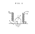
- a cooling cylinder 11 composed of copper or a metal having a heat conductivity larger than that of copper, forcibly cooled by circulation of a cooling medium, extending from an upper part of the main chamber toward the raw material melt surface and cooling neighborhood of the crystal growth interface.
- a hollow cooling cylinder 11a in a cylindrical shape having a hollow structure (refer to Fig.
- the hollow cooling cylinder 11a or cooling cylinder 11b with a cooling pipe extends, for example, from a ceiling of the main chamber 1 toward a raw material melt surface so as to surround a single crystal ingot 3 under pulling, and its end is disposed in the vicinity of the crystal growth interface 22.
- the cooling cylinder 11 is forcibly cooled with the cooling medium and disposedin the vicinity of the crystal growth interface 22, i.e., at a position immediately above and close to the melt surface.
- the cooling medium can be circulated only at a position remote from the melt surface.
- a crystal immediately after the growth can be forcibly cooled by a cooling cylinder in which the cooling medium is directly circulated at a position extremely near the crystal growth interface, and thus extremely high cooling effect can be obtained.
- a cooling medium is introduced from a cooling medium inlet 12, circulates in the cooling cylinder to forcibly cool the cooling cylinder, and then discharged to the outside.
- the discharged cooling medium is cooled by a heat exchanger, supplied to the cooling cylinder again and circulates through it.
- any liquid or gas conventionally used as a cooling medium can be used as the cooling medium, it is suitable to use water in view of handling property, cost and so forth in addition to the cooling characteristics thereof. Further, by controlling flow rate and temperature of the cooling medium passing through the cooling cylinders as required, the heat quantity of the cooling cylinder to be removed can be changed, and therefore a desired cooling atmosphere according to the single crystal growth rate can be formed. Further, it is also possible to change temperature distribution in a crystal under pulling by changing winding density distribution of the cooling pipe shown in Fig. 2.
- the material of the cooling cylinder copper or a metal having a heat conductivity larger than that of copper is used, which is particularly excellent in heat conductivity.
- the latter include silver, silver-copper alloys and so forth. The reasons why these copper and so forth are employed were explained in (Experiment 1) and (Experiment 2) described above. That is, the temperature of the cooling cylinder or the cooling pipe can be 100°C or lower if they are forcibly cooled directly with water, and therefore the surface of the cooling cylinder is not melted or damaged.
- the cooling cylinder made of copper or the like has excellent heat resistance and, in. addition, extremely high heat conductivity as described above. Therefore, after absorbing heat emitted from the single crystal ingot, it efficiently transfer the heat to the cooling medium such as water circulating through inside of the cooling cylinder, and lowers the temperature around the crystal. Thus, the cooling rate of a single crystal can be markedly improved.
- the shape of the cooling cylinder according to the present invention is not limited to those, shown in the aforementioned Figs. 1 and 2.
- a so-called baffle plate may also be provided in the hollow so as to enable uniform and efficient cooling.
- the outer surface of the cooling cylinder may be covered with a copper plate so that the cooling pipe should not be exposed on the surface.
- the cooling cylinder according to the present invention has such a structure that neighborhood of the crystal growth interface should be forcibly cooled, and the total region from the neighborhood of the crystal growth interface to the ceiling of the main chamber may not be forcibly cooled.
- the cooling cylinders shown in Figs. 1 and 2 have a cylindrical shape only in the approximately perpendicular direction, the cooling cylinder may have, for example, such a shape that the end portion should be parallel to the melt surface.
- the crucible and the cooling cylinder are preferably disposed so that Distance A (mm) between the lower end of the cooling cylinder made of copper or the like and the raw material melt surface and Distance B (mm) between the lower end of the cooling medium circulating in the cooling cylinder and the raw material melt surface should satisfy the relationships of 100 ⁇ B ⁇ A ⁇ 5 and B - A ⁇ 50. If a single crystal is pulled with adjusting a position of the melt surface so that the relationships should be satisfied, the forced cooling effect is surely exerted, and thus the crystal growth rate can be accelerated. In addition, the end of the cooling cylinder is not damaged by the melt.
- the end of the cooling cylinder and the lower end of the cooling medium circulating in the cooling cylinder are preferably separated from the raw material melt surface by 5 mm or more.
- the effect of rapidly cooling the crystal is more improved as the cooling cylinder becomes closer to the melt surface, the end of the cooling cylinder may be brought into contact with the melt surface when the melt surface is vibrated, if the cooling cylinder is brought close exceeding the distance defined above.
- the cooling effect of the crystal is decreased, and therefore a distance of 100 mm or less is preferred.
- the relationship of B - A ⁇ 50 is defined for the following reasons.
- cooling cylinder 11 in the manner described above, gas flow guide effect for inert gas such as argon that is passed through the inside of the cooling cylinder from its upper part can be increased, and cooling effect by the gas can also be obtained.
- inert gas such as argon
- the cooling cylinder in the main chamber, while it is easy to dispose it so that it should extend from the ceiling of the main chamber 1 toward the melt surface as shown in the drawings, it may also be fixed on the side wall of the main chamber.
- thermal history of a growing single crystal can be freely controlled by changing the position of the melt surface with respect to the cooling cylinder. For example, if the cooling cylinder and the melt surface are brought closer, rapid cooling effect can be obtained. Conversely, if the cooling cylinder is made remoter from the melt surface, gradual cooling effect can be obtained. Therefore, by controlling the positions of the cooling cylinder and the melt surface, it is also possible to control the aggregation temperature zone of crystal defects called grown-in defects and the temperature zone concerning the oxygen precipitation in the crystal to be in a desired region. In order to freely perform such control during the crystal growth, there may be provided a driving mechanism for moving the cooling cylinder upwardly and downwardly.
- the apparatus of the present invention in the pulling methods under magnetic field (referred to as "MCZ method” hereafter) in which an electromagnet (not shown in the drawings) is provided outside the main chamber 1 containing the melt 4 and the single crystal 3 is grown with applying a magnetic field to the melt' 4 4 in the chamber, and thereby a similar effect can of course be obtained.
- MCZ method magnetic field
- the apparatus of the present invention is used as an apparatus for growing a single crystal by the MCZ method for the production of a large single crystal, the crystal growth rate can be more effectively improved and therefore marked improvement of productivity can be expected.
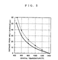
- Fig. 5 shows temperature distributions of crystals under pulling having a diameter of 8 inches along the pulling axis direction, which were calculated by the simulation.
- the thick line represents the result for the case of usingsuch an apparatus for growing a single crystal provided with a cooling cylinder according to the present invention as shown in Fig. 1, in which temperature of the cooling cylinder was assumed to be fixed at 30°C and distance between a melt surface and the cooling cylinder was set to be 50 mm.
- the fine line represents the result for an HZ structure provided with a cooling cylinder only of which upper part is cooled with water and having a heat insulating material of a conventionally used particular structure at a lower part, in which distance between a melt surface and the heat insulating material was set to be 17 mm.
- the structure of the present invention exerts markedly higher cooling effect compared with the conventional structure.
- the temperature gradient G (K/cm) of the crystal under pulling in the neighborhood of the crystal growth interface between the melting point and 1400.°C is calculated to be 52.3 (K/cm) at the crystal center for the structure of the present invention, which was markedly larger than the value for the conventional structure, 36.6.
- Fig. 6 is a graph showing a relationship of the aforementioned temperature gradient G and the maximum pulling rate (actually measured value) of a crystal .(diameter: 8 inches) as a product that can be produced in a large scale for the case of using an apparatus for growing a single crystal having a. conventionally used HZ structure.
- a silicon single crystal ingot was grown by the MCZ method using the apparatus 20 for growing a single crystal shown in Fig. 1 provided with an electromagnet (not shown in the drawing) outside the main chamber 1.
- the cooling cylinder 11 was a hollow cooling cylinder 11a, of which material was. copper, and water was used as a cooling medium. The end of the cooling cylinder 11 was brought close to the melt surface so that the distance separating them should be 20 mm to perform the operation.
- a magnetic field was applied to the silicon melt 4 so that the magnetic field strength at the center of horizontal magnetic field should be 4000 G, and a hot zone that could contain a crucible having a diameter of 24 inches was used.
- the average pulling rate is usually about 1.8 mm/min at most for a diameter of 8 inches. Therefore, compared with this rate, the average pulling rate was markedly increased.
- Example 2 150 kg of polycrystal silicon raw material was introduced into its crucible having a diameter of 32 inches, and a single crystal having a diameter of 12 inches (300 mm) and a length of constant diameter portion of about 45 cm was grown.
- a silicon single crystal in an approximately cylindrical shape could be obtained at an average pulling rate of 1.6 mm/min for the constant diameter portion of the single crystal without any deformation. This means that there was achieved a pulling rate about.2 times of the pulling rate obtained in Comparative Example 2.
- Single crystals were grown under the same conditions as used in Example 1 except that used was an apparatus for growing a single crystal in which a graphite cylinder was suspended from the ceiling of the main chamber in which any cooling medium was not circulated instead of the cooling cylinder of the apparatus for growing a single crystal used in the aforementioned example.
- the lengths of the grown single crystals were also approximately the same as the lengths pulled in the example.
- any single crystal could not be normally grown at a pulling rate higher than the above level, because there were caused problems, for example, crystal was deformed during the growth, slip dislocations were generated and so forth.
Landscapes
- Chemical & Material Sciences (AREA)
- Engineering & Computer Science (AREA)
- Crystallography & Structural Chemistry (AREA)
- Materials Engineering (AREA)
- Metallurgy (AREA)
- Organic Chemistry (AREA)
- Crystals, And After-Treatments Of Crystals (AREA)
- Liquid Deposition Of Substances Of Which Semiconductor Devices Are Composed (AREA)
Abstract
Description
Claims (8)
- A method for growing a single crystal by the Czochralski method, wherein a single crystal is grown with forced cooling of neighborhood of a crystal growth interface by disposing a cooling cylinder formed of copper or a metal having a heat conductivity larger than that of copper at least in the vicinity of the crystal growth interface so as to surround the single crystal under pulling and circulating a cooling medium in the cooling cylinder.
- The method for growing a single crystal according to Claim 1, wherein the single crystal is pulled with adjusting a position of the melt surface so that Distance A (mm) between a lower end of the cooling cylinder and the raw material melt surface and Distance B (mm) between a lower end of the cooling medium circulating in the cooling cylinder and the raw material melt surface should satisfy a relationship of 100 ≧ B ≧ A ≧ 5.
- The method for growing a single crystal according to Claim 2, wherein Distance A and Distance B satisfy a relationship of B - A ≦ 50.
- An apparatus for growing a single crystal based on the Czochralski method comprising at least a main chamber enclosing a crucible for containing a raw material melt and a heater for heating the raw material melt, a pulling chamber continuously provided above the main chamber, into which a grown single crystal is pulled and stored, and a cooling cylinder surrounding the single crystal under pulling, wherein at least the cooling cylinder is composed of copper or a metal having a heat conductivity larger than that of copper, is forcibly cooled by circulation of a cooling medium, and extends from an upper portion of the main chamber toward a raw material melt surface so as to cool neighborhood of a crystal growth interface.
- The apparatus for growing a single crystal according to Claim 4, wherein the cooling cylinder has a hollow structure for circulation of the cooling medium, or consist of a solid cooling cylinder wound with a cooling pipe for circulation of the cooling medium.
- The apparatus for growing a single crystal according to Claim 4 or 5, wherein the cooling medium is water.
- The apparatus for growing a single crystal according to any one of Claims 4 to 6, wherein Distance. A (mm) between the lower end of the cooling cylinder and the raw material melt surface and Distance B (mm) between a lower end of the cooling medium circulating in the cooling cylinder and the raw material melt surface satisfy a relationship of 100 ≧ B ≧ A ≧ 5 during pulling of the crystal.
- The apparatus for growing a single crystal according to Claim 7, wherein Distance A and Distance B satisfy a relationship of B- A ≦50.
Applications Claiming Priority (3)
| Application Number | Priority Date | Filing Date | Title |
|---|---|---|---|
| JP2000401648A JP4055362B2 (en) | 2000-12-28 | 2000-12-28 | Single crystal growth method and single crystal growth apparatus |
| JP2000401648 | 2000-12-28 | ||
| PCT/JP2001/011491 WO2002053811A1 (en) | 2000-12-28 | 2001-12-26 | Method and apparatus for growing single crystal |
Publications (2)
| Publication Number | Publication Date |
|---|---|
| EP1347082A1 true EP1347082A1 (en) | 2003-09-24 |
| EP1347082A4 EP1347082A4 (en) | 2008-04-09 |
Family
ID=18866049
Family Applications (1)
| Application Number | Title | Priority Date | Filing Date |
|---|---|---|---|
| EP01272881A Ceased EP1347082A4 (en) | 2000-12-28 | 2001-12-26 | Method and apparatus for growing single crystal |
Country Status (7)
| Country | Link |
|---|---|
| US (1) | US6899758B2 (en) |
| EP (1) | EP1347082A4 (en) |
| JP (1) | JP4055362B2 (en) |
| KR (1) | KR100825997B1 (en) |
| CN (1) | CN1265030C (en) |
| TW (1) | TWI225902B (en) |
| WO (1) | WO2002053811A1 (en) |
Families Citing this family (24)
| Publication number | Priority date | Publication date | Assignee | Title |
|---|---|---|---|---|
| JP4569090B2 (en) * | 2003-10-10 | 2010-10-27 | 信越半導体株式会社 | Single crystal manufacturing method, single crystal, and single crystal manufacturing apparatus |
| WO2005073439A1 (en) * | 2004-02-02 | 2005-08-11 | Shin-Etsu Handotai Co., Ltd. | Silicon single crystal, silicon wafer, production apparatus therefor and process for producing the same |
| JP4255972B2 (en) * | 2004-06-11 | 2009-04-22 | 日本電信電話株式会社 | Crystal manufacturing method and apparatus |
| CN100383295C (en) * | 2006-03-31 | 2008-04-23 | 浙江大学 | Automatic Control Method of Czochralski Crystal Growth Furnace |
| JP4919343B2 (en) * | 2007-02-06 | 2012-04-18 | コバレントマテリアル株式会社 | Single crystal pulling device |
| JP4829176B2 (en) * | 2007-06-08 | 2011-12-07 | シルトロニック・ジャパン株式会社 | Single crystal manufacturing method |
| KR100983195B1 (en) * | 2007-12-28 | 2010-09-20 | 주식회사 실트론 | 2-Dimensional Line-Defects Controlled Silicon Ingot, Wafer, Epitaxial Wafer, and Manufacturing Process and Apparatus Therefor |
| JP4582149B2 (en) * | 2008-01-10 | 2010-11-17 | 信越半導体株式会社 | Single crystal manufacturing equipment |
| JP5186970B2 (en) * | 2008-03-24 | 2013-04-24 | 信越半導体株式会社 | Single crystal manufacturing apparatus and method |
| US8821636B2 (en) * | 2008-05-20 | 2014-09-02 | Shin-Etsu Handotai Co., Ltd. | Single-crystal manufacturing apparatus |
| US8012255B2 (en) * | 2008-07-31 | 2011-09-06 | Sumco Phoenix Corporation | Method and apparatus for controlling diameter of a silicon crystal ingot in a growth process |
| US20100024717A1 (en) * | 2008-07-31 | 2010-02-04 | Benno Orschel | Reversed action diameter control in a semiconductor crystal growth system |
| US8221545B2 (en) * | 2008-07-31 | 2012-07-17 | Sumco Phoenix Corporation | Procedure for in-situ determination of thermal gradients at the crystal growth front |
| KR101266701B1 (en) * | 2010-02-12 | 2013-05-22 | 주식회사 엘지실트론 | Cooling Apparatus of Silicon Crystal and Single Crystal Grower including the same |
| JP5904079B2 (en) | 2012-10-03 | 2016-04-13 | 信越半導体株式会社 | Silicon single crystal growing apparatus and silicon single crystal growing method |
| CN102978690A (en) * | 2012-12-24 | 2013-03-20 | 苏州工业园区杰士通真空技术有限公司 | Novel sapphire crystal growth furnace body cooling system |
| CN103710742A (en) * | 2013-12-30 | 2014-04-09 | 上海涌真机械有限公司 | Single crystal furnace capable of improving czochralski-method single crystal growth speed |
| CN105002556A (en) * | 2014-04-21 | 2015-10-28 | 洛阳金诺机械工程有限公司 | Device for raising crystallization velocity of silicon core during drawing of silicone core |
| CN107604431A (en) * | 2016-07-11 | 2018-01-19 | 上海超硅半导体有限公司 | N-type monocrystalline silicon manufacturing method and apparatus |
| KR101734906B1 (en) | 2016-10-05 | 2017-05-12 | 송철현 | Puller for sapphire growth device |
| JP6825728B1 (en) * | 2020-01-10 | 2021-02-03 | 信越半導体株式会社 | Single crystal manufacturing equipment |
| US12104275B2 (en) | 2022-08-01 | 2024-10-01 | Globalwafers Co., Ltd. | Ingot puller apparatus having cooling jacket device with cooling fluid tubes |
| WO2024032353A1 (en) * | 2022-08-09 | 2024-02-15 | 隆基绿能科技股份有限公司 | Single crystal furnace, heat conduction tool, and crystal pulling control method for single crystal furnace |
| CN116428902B (en) * | 2023-06-09 | 2023-08-22 | 苏州晨晖智能设备有限公司 | Single crystal furnace double-phase composite heat exchanger, single crystal furnace and heat exchange method |
Family Cites Families (8)
| Publication number | Priority date | Publication date | Assignee | Title |
|---|---|---|---|---|
| JPS63285187A (en) * | 1987-05-15 | 1988-11-22 | Toshiba Ceramics Co Ltd | Apparatus for pulling up silicon single crystal |
| JP2953697B2 (en) * | 1988-10-05 | 1999-09-27 | 三菱マテリアル株式会社 | Silicon single crystal pulling device |
| US4981549A (en) * | 1988-02-23 | 1991-01-01 | Mitsubishi Kinzoku Kabushiki Kaisha | Method and apparatus for growing silicon crystals |
| JP3220542B2 (en) * | 1993-01-05 | 2001-10-22 | ワッカー・エヌエスシーイー株式会社 | Semiconductor single crystal rod manufacturing equipment |
| DE19503357A1 (en) * | 1995-02-02 | 1996-08-08 | Wacker Siltronic Halbleitermat | Device for producing a single crystal |
| US6503594B2 (en) * | 1997-02-13 | 2003-01-07 | Samsung Electronics Co., Ltd. | Silicon wafers having controlled distribution of defects and slip |
| JP3992800B2 (en) * | 1997-09-22 | 2007-10-17 | Sumco Techxiv株式会社 | Single crystal manufacturing apparatus and single crystal manufacturing method |
| JP4195738B2 (en) * | 1998-04-08 | 2008-12-10 | Sumco Techxiv株式会社 | Single crystal manufacturing equipment |
-
2000
- 2000-12-28 JP JP2000401648A patent/JP4055362B2/en not_active Expired - Fee Related
-
2001
- 2001-12-26 US US10/203,825 patent/US6899758B2/en not_active Expired - Lifetime
- 2001-12-26 WO PCT/JP2001/011491 patent/WO2002053811A1/en not_active Ceased
- 2001-12-26 EP EP01272881A patent/EP1347082A4/en not_active Ceased
- 2001-12-26 KR KR1020027011272A patent/KR100825997B1/en not_active Expired - Fee Related
- 2001-12-26 CN CNB018057594A patent/CN1265030C/en not_active Expired - Lifetime
- 2001-12-28 TW TW090132905A patent/TWI225902B/en not_active IP Right Cessation
Also Published As
| Publication number | Publication date |
|---|---|
| CN1265030C (en) | 2006-07-19 |
| KR20020081369A (en) | 2002-10-26 |
| JP2002201090A (en) | 2002-07-16 |
| US20030010276A1 (en) | 2003-01-16 |
| KR100825997B1 (en) | 2008-04-29 |
| TWI225902B (en) | 2005-01-01 |
| WO2002053811A1 (en) | 2002-07-11 |
| CN1406291A (en) | 2003-03-26 |
| EP1347082A4 (en) | 2008-04-09 |
| JP4055362B2 (en) | 2008-03-05 |
| US6899758B2 (en) | 2005-05-31 |
Similar Documents
| Publication | Publication Date | Title |
|---|---|---|
| US6899758B2 (en) | Method and apparatus for growing single crystal | |
| US6632280B2 (en) | Apparatus for growing single crystal, method for producing single crystal utilizing the apparatus and single crystal | |
| US9217208B2 (en) | Apparatus for producing single crystal | |
| EP1084286B1 (en) | Electrical resistance heater for crystal growing apparatus | |
| US20190136407A1 (en) | Single crystal ingots with reduced dislocation defects and methods for producing such ingots | |
| US5714004A (en) | Process for producing polycrystalline semiconductors | |
| EP0349904B1 (en) | Apparatus for casting silicon | |
| JP2009505935A (en) | Apparatus and method for crystal growth | |
| KR101540225B1 (en) | Single Crystal Manufacturing Apparatus and Single Crystal Manufacturing Method | |
| JP4389574B2 (en) | SiC single crystal manufacturing method and manufacturing apparatus | |
| KR20110036896A (en) | Single crystal production device and single crystal production method | |
| EP1801268B1 (en) | Magnetic field application method of pulling silicon single crystal | |
| EP1614774A1 (en) | Process for producing single crystal | |
| JP3678129B2 (en) | Crystal growth method | |
| JP4175008B2 (en) | Single crystal growth method | |
| JP5051044B2 (en) | Method for growing silicon single crystal | |
| JPH07206576A (en) | Silicon single crystal manufacturing equipment | |
| KR20010052460A (en) | Electrical resistance heater for crystal growing apparatus | |
| JPH0952790A (en) | Single crystal growing apparatus and single crystal growing method | |
| JPWO2001057293A1 (en) | Single crystal growth apparatus, single crystal manufacturing method using the apparatus, and single crystal | |
| JPH0416587A (en) | Single crystal pulling up device | |
| JPH03131591A (en) | Method for growing crystal and device for dissolving crystal raw material |
Legal Events
| Date | Code | Title | Description |
|---|---|---|---|
| PUAI | Public reference made under article 153(3) epc to a published international application that has entered the european phase |
Free format text: ORIGINAL CODE: 0009012 |
|
| 17P | Request for examination filed |
Effective date: 20020822 |
|
| AK | Designated contracting states |
Kind code of ref document: A1 Designated state(s): AT BE CH CY DE DK ES FI FR GB GR IE IT LI LU MC NL PT SE TR |
|
| RBV | Designated contracting states (corrected) |
Designated state(s): AT BE CH CY DE FR GB IT LI |
|
| A4 | Supplementary search report drawn up and despatched |
Effective date: 20080312 |
|
| RAP1 | Party data changed (applicant data changed or rights of an application transferred) |
Owner name: SHIN-ETSU HANDOTAI CO., LTD. |
|
| RBV | Designated contracting states (corrected) |
Designated state(s): DE FR GB IT |
|
| 17Q | First examination report despatched |
Effective date: 20090922 |
|
| REG | Reference to a national code |
Ref country code: DE Ref legal event code: R003 |
|
| STAA | Information on the status of an ep patent application or granted ep patent |
Free format text: STATUS: THE APPLICATION HAS BEEN REFUSED |
|
| 18R | Application refused |
Effective date: 20131126 |