TECHNICAL FIELD
The present invention relates to an organic
electric-field light-emitting element (hereinafter referred
to as an organic electroluminescent (EL) element) and, more
particularly to an organic EL element suitably employed in
display devices for personal and industrial use, light
sources of printer heads and the like.
BACKGROUND ART
Japanese Patent Laid-open Nos. H2(1990)-139893,
H2(1990)-196475 and H2(1990)-196475 disclose an organic EL
element provided with an inorganic semiconductive thin
layer and an organic luminescent layer between electrodes
for easier injection of electrons and the like. In the
organic EL element, an inorganic semiconductive thin layer
is formed on an anode, and an organic luminescent layer and
a cathode are further formed thereon, which inorganic
semiconductive thin layer is made of an inorganic
semiconductive material such as carbon, germanium, silicon,
tin, silicon carbide, boron nitride, boron phosphide and
gallium nitride.
Japanese Patent Laid-open Nos. H10(1998)-88120 and
2000-150161 disclose an organic EL element being of
structure, positive hole injecting layer/luminescent
layer/electron-injecting layer for improving its luminance
(luminescent brightness). Amine materials capable of
transporting positively charged holes (hereinafter referred
to as positive holes) are used as a luminescent material,
and tris(8-hydroxyquinolinate)aluminum(Alq), bis(2-methyl-8-hydroxyquinolinate)(p-cyanophenolate)gallium
and the like
are used in the electron-injecting layer.
However, in the organic EL elements disclosed by
H2(1990)-139893 and H2(1990)-196475, the mobility of
electrons injected from the cathode is relatively reduced
by the inorganic semiconductive thin layer, resulting in a
decrease in luminous efficiency. On other words, although
electrons are desired to recombine with positive holes
around the center of the organic luminescent layer for
efficient luminescence, they may re-couple around the
inorganic semiconductive thin layer, thereby losing
luminescence or reducing the ratio of re-coupling.
Consequently, the luminescence in the organic luminescent
layer is decreased.
In the organic EL elements disclosed by H10(1998)-88120
and 2000-150161, the materials capable of injecting
electrons such as Alq, which are used in the electron
injecting layer, are liable to be degraded with shorter
half-lives.
The inventors have made efforts to solve the above
problems and then found that an organic EL element can be
obtained of which luminance is higher even at low voltages,
e.g., direct current 10V, and half-life is remarkably
lengthened by certain structures. According to a first
structure, an inorganic compound layer is provided between
an organic luminescent layer and a cathode layer, and
certain aromatic amine compounds are used in the organic
luminescent layer. According to a second structure, a layer
containing a reductive dopant (hereinafter referred to as a
reductive dopant layer) is provided between an organic
luminescent layer and a cathode layer, and certain aromatic
amine compounds are used in the organic luminescent layer.
According to a third structure, a certain electron
injecting layer is provided between an organic luminescent
layer and an anode, and certain aromatic amine compounds
are used in the organic luminescent layer.
An object of the present invention is therefore to
provide an organic EL element with high luminance even at
low driving voltages, and with remarkable long half-life.
SUMMARY OF THE INVENTION
According to a first aspect of the present
invention, an organic EL element is provided which
comprises an anode layer, an organic luminescent layer, a
cathode layer and an inorganic compound layer between the
organic luminescent layer and the cathode layer. According
to a second aspect of the present invention, an organic EL
element is provided which comprises an anode layer, an
organic luminescent layer, a cathode layer and a reductive
dopant layer between the organic luminescent layer and the
cathode layer. In these organic EL elements, the organic
luminescent layers comprise an aromatic amine compound
represented by the following formula (1) and/or an aromatic
amine compound represented by the following formula (2).
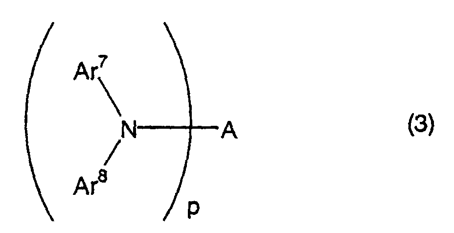
According to a third aspect of the present
invention, an organic EL element is provided which
comprises an anode layer, an organic luminescent layer, a
cathode layer and an electron injecting layer between the
organic luminescent layer and the cathode layer. The
electron injecting layer comprises a hydrocarbon compound
with an anthracene nucleus or a fluoranthene nucleus. The
energy gap of the compound is 2.7 eV or more. Further, the
organic luminescent layer comprises an aromatic amine
compound represented by the following formula (3) and/or an
aromatic amine compound represented by the following
formula (4).
That is, according to the first to third aspects,
an organic EL element can be provided which contains as a
luminescent material an aromatic amine compound with at
least three condensed aromatic rings. Here "at least three
condensed aromatic rings" means that at least three
aromatic rings are condensed.
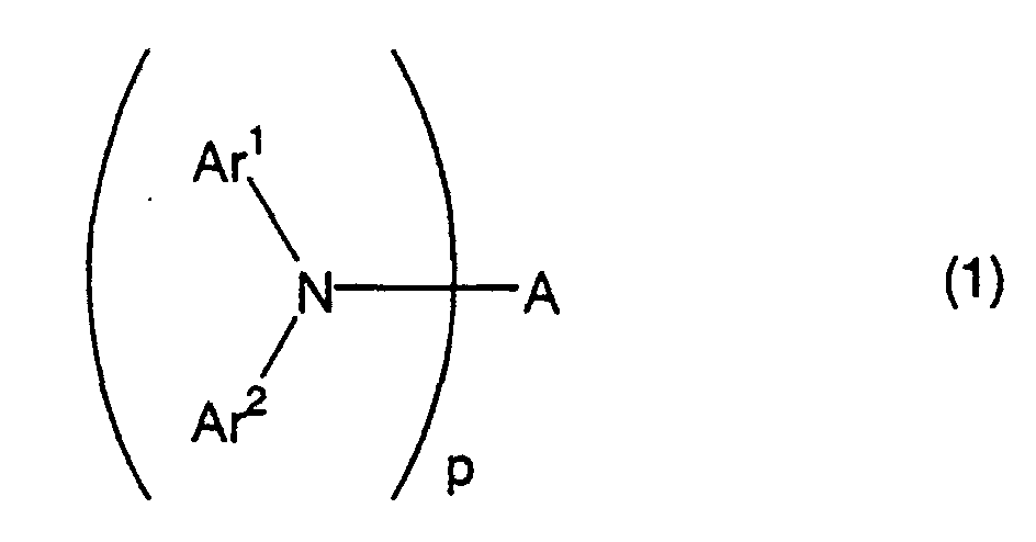
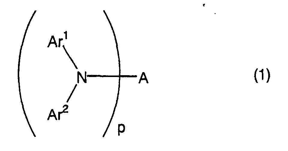
wherein A, Ar
1 and Ar
2 are independently a substituted or
unsubstituted C
6-60 aromatic group which does not contain a
styryl group nor an alkenyl group, at least one of A, Ar
1
and Ar
2 contains substituted or unsubstituted at least three
condensed aromatic rings, and p of a condensation number is
an integer of 1 to 6.
wherein B, Ar
3, Ar
4, Ar
5 and Ar
6 are independently a
substituted or unsubstituted C
6-60 aromatic group which does
not contain a styryl group nor an alkenyl group, at least
one of B, Ar
3, Ar
4, Ar
5 and Ar
6 contains substituted or
unsubstituted at least three condensed aromatic rings, and
q and r of a condensation number are an integer of 1 to 6.
wherein A, Ar
7 and Ar
8 are independently a substituted or
unsubstituted C
6-60 aromatic group, at least one of A, Ar
7
and Ar
8 contains substituted or unsubstituted at least three
condensed aromatic rings, and p of a condensation number is
an integer of 1 to 6.
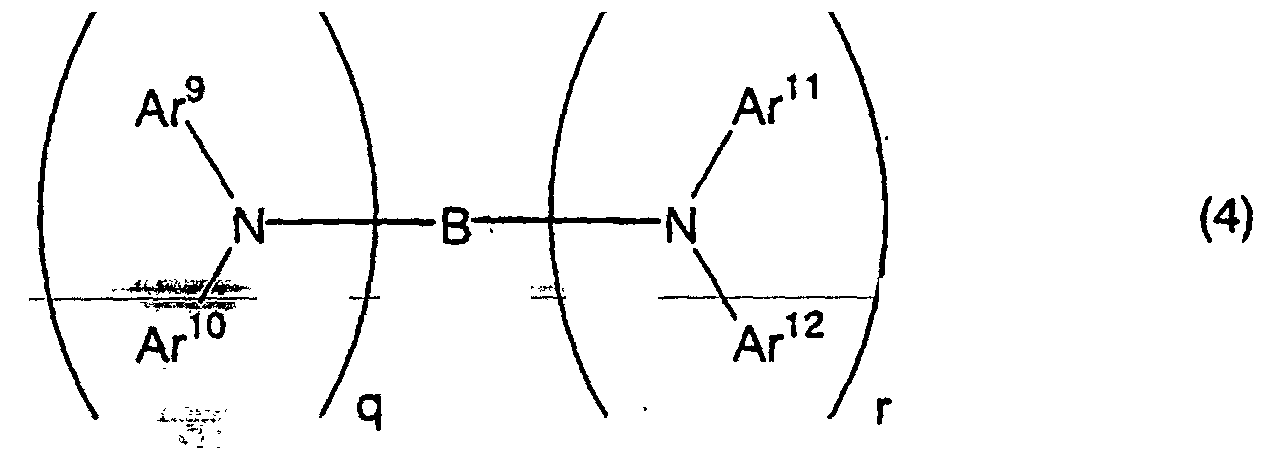
wherein B, Ar
9, Ar
10, Ar
11 and Ar
12 are independently a
substituted or unsubstituted C
6-60 aromatic group, at least
one of B, Ar
9, Ar
10, Ar
11 and Ar
12 contains substituted or
unsubstituted at least three condensed aromatic rings, and
q and r of a condensation number are an integer of 1 to 6.
In the aromatic amine compounds of the formulas (1)
to (4), Ar1 to Ar12 may be the same as or different from each
other, and preferably have 6 to 40 carbon atoms. A and B
preferably contain substituted or unsubstituted at least
three condensed aromatic rings
BRIEF DESCRIPTION OF THE DRAWINGS
Fig. 1 is a sectional view of an organic EL element
according to a first embodiment.
Fig. 2 is a sectional view of an organic EL element
according to a second embodiment.
Fig. 3 is a sectional view of an organic EL element
according to a third embodiment.
BEST MODE OF CARRYING OUT THE INVENTION
An embodiment of the present invention will be
explained with reference to the drawings. These drawings
diagrammatically show the sizes, shapes and positions of
constituent members for easy understanding of the present
invention. The present invention is not thus limited to the
drawings. In the drawings, hatching representing a section
may be omitted.
[First Embodiment]
A first embodiment of the organic EL element
according to the present invention will be described with
reference to Fig. 1. Fig. 1 is a sectional view of an
organic EL element 100, showing the structure of an anode
layer 10, an organic luminescent layer 12, an inorganic
compound layer 14 and a cathode layer 16 laminated on a
substrate (not shown) in this order.
Here, the organic luminescent layer 12 and
inorganic compound layer 14 will be mainly described since
they are features of the first embodiment. The other
members such as the anode layer 10 and cathode layer 16
will be briefly described about their structures and
manufacturing methods. For the members particularly not
described, they can be of structure known in the art and
manufactured by methods known in the art.
(1) Organic luminescent layer
(i) Materials 1
The above-mentioned aromatic amine compounds of the
formulas (1) and (2) are used in an organic luminescent
layer. The use of such aromatic amine compounds allows
excellent luminance at low voltages, e.g., about 10V when
an inorganic compound layer is provided.
Further, the aromatic amine compounds of the
formulas (1) and (2) do not contain any substituent with a
styryl group or an alkenyl group. By not containing such a
substituent, the half-life of the organic EL element can be
extended.
If Ar1 and Ar2 are the same in the formula (1), the
compounds of the formula (1) can be of symmetric structure.
Similarly if Ar3 and Ar5 are the same and Ar4 and Ar6 are the
same in the formula (2), the compounds of the formula (2)
can be of symmetric structure.
By containing such a symmetric compound, the half-life
can be remarkably extended.
Condensed aromatic rings contained in the compounds
of the formulas (1) and (2) are at least three condensed
aromatic rings having a bone structure such as pyrene,
perylene, anthracene, fluoranthene, chrycene, rubicene,
tetracene, pentacene, tetrabenzophenanthrene,
tetrabenzanthracene, tetrabenzofluorene, benzoperylene,
dibenzopyrene, dibenzochrycene, dibenzoperylene,
benzotetracene, decacyclene, acenaphthofluoranthene and
dibenzofluoranthene.
Preferable bone structures include pyrene, perylene,
anthracene, fluoranthene, chrycene, rubicene, tetracene,
pentacene, tetrabenzophenanthrene, tetrabenzanthracene,
tetrabenzofluorene, benzoperylene, dibenzopyrene,
dibenzochrycene, dibenzoperylene, benzotetracene,
decacyclene, acenaphthofluoranthene and dibenzofluoranthene.
(ii) Materials 2
The above-mentioned aromatic amine compounds of the
formulas (1) and (2) may preferably have a substituent such
as cyano groups, halogen groups, linear, branched or cyclic
alkyl groups, linear, branched or cyclic alkoxy groups,
substituted or unsubstituted aryl groups, substituted or
unsubstituted aryloxy groups, COOR wherein R represents a
hydrogen atom, an alkyl group, an aryl group or an aralkyl
group, and substituted or unsubstituted arylthio groups.
Preferable substituents include halogen groups such
as fluorine atom, chlorine atom and the like; linear,
branched or cyclic C1-8 alkyl groups such as methyl group,
ethyl group, n-propyl group, isopropyl group, n-butyl group,
isobutyl group, tert-butyl group, n-pentyl group, isopentyl
group, neopentyl group, tert-pentyl group, n-hexyl group,
cyclohexyl group, n-heptyl group, cyclohexylmethyl group,
n-octyl group, tert-octyl group, 2-ethylhexyl group and the
like; linear, branched or cyclic C1-8 alkoxy groups such as
methoxy group, ethoxy group, n-propoxy group, isopropoxy
group, n-butoxy group, isobutoxy group, n-pentyloxy group,
isopentyloxy group, neopentyloxy group, n-hexyloxy group,
cyclohexyloxy group, n-heptyloxy group, cyclohexylmethyloxy
group, n-octyloxy group, 2-ethylhexyloxy group and the
like; substituted or unsubstituted C6-10 aryl groups such as
phenyl group, 2-methylphenyl group, 3-methylphenyl group,
4-methylphenyl group, 4-ethylphenyl group, 4-n-propylphenyl
group, 4-tert-butylphenyl group, 2-methoxyphenyl group, 4-methoxyphenyl
group, 3-ethoxyphenyl group, 3-fluorophenyl
group, 4-chlorophenyl group, 1-naphtyl group, 2-naphtyl
group and the like; COOR wherein R represents a hydrogen
atom; a linear, branched or cyclic C1-8 alkyl group such as
methyl group, ethyl group, n-propyl group, isopropyl group,
n-butyl group, isobutyl group, tert-butyl group, n-pentyl
group, isopentyl group, neopentyl group, tert-pentyl group,
n-hexyl group, cyclohexyl group, n-heptyl group,
cyclohexylmethyl group, n-octyl group, tert-octyl group, 2-ethylhexyl
group and the like; a substituted or
unsubstituted C6-10 aryl group such as phenyl group, 2-methylphenyl
group, 3-methylphenyl group, 4-methylphenyl
group, 4-ethylphenyl group, 4-n-propylphenyl group, 4-tert-butylphenyl
group, 2-methoxyphenyl group, 4-methoxyphenyl
group, 3-ethoxyphenyl group, 3-fluorophenyl group, 4-chlorophenyl
group, 1-naphtyl group, 2-naphtyl group and
the like; or a substituted or unsubstituted C7-10 aralkyl
group such as benzyl group, phenethyl group, 2-methylbenzyl
group, 3-methylbenzyl, 4-methylbenzyl group, 3-fluorobenzyl
group, 2-chlorobenzyl group, 4-chlorobenzyl group, 4-methoxybenzyl
group and the like.
Preferable aromatic amine compounds of the formulas
(1) and (2) include:
9,10-bis[4'(dl-p-tolylamino)phenyl]anthracene
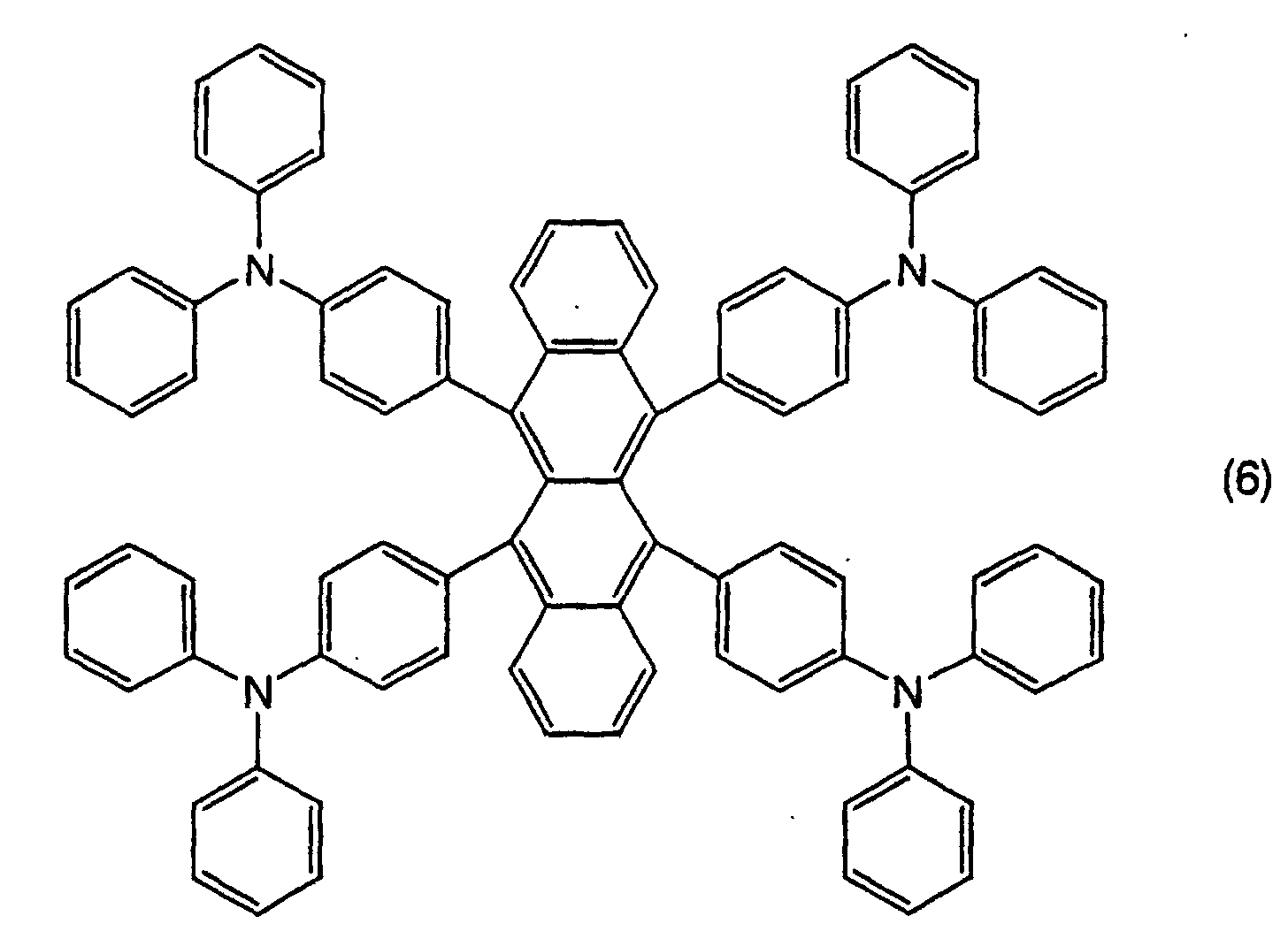
5,6,11,12-tetrakis[4'-(diphenylamino)phenyl]naphthacene
5,11-bis(diphenylamino)tetracene
5,6-diphenyl-11,12-bis[4'-(diphenylamino)phenyl]naphthacene
3,9-bis(di-p-tolylamino)perylene
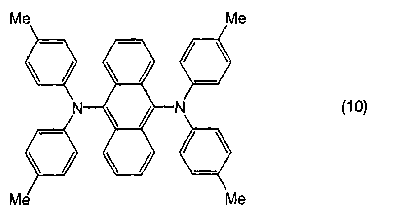
9,10-bis(di-p-tolylamino)anthracene
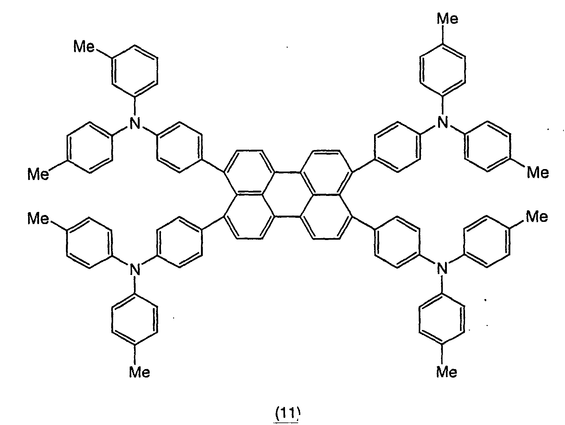
3,4,9,10-tetrakis(4'-(di-p-tolylamino)phenyl]perylene
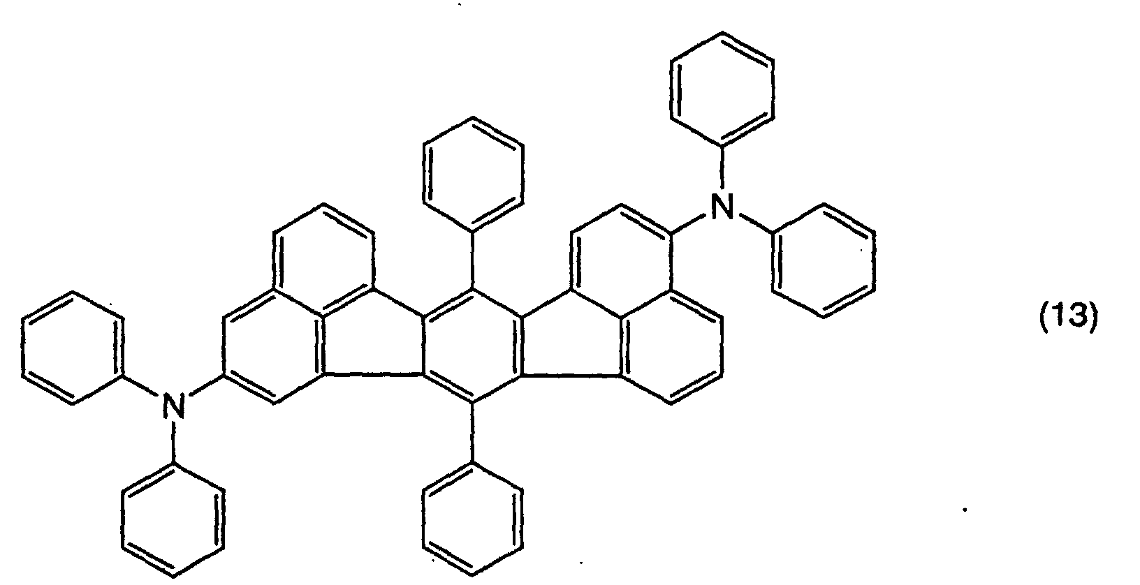
3,11-bis(diphenylamino)-7,14-diphenylacenaphtho(1,2-k)fluoranthene
3,10-bis(diphenylamino)-7,14-diphenylacenaphtho(1,2-k)fluoranthene
3,11-bis(di-p-tolylamino)-7,14-diphenylacenaphtho(1,2-k)fluoranthene
The aromatic amine compounds of the above formulas
(5) to (14) are referred to as compounds 1 to 10 in
Examples, respectively.
(iii) Electron Mobility
The electron mobility of an organic luminescent
material in an organic luminescent layer is preferably 1×
10-7 cm2/V·s or more. If less than 1×10⁻⁷ cm2/V·s, a high-speed
response in an organic EL element may become
difficult and its luminance may decrease.
The electron mobility of an organic luminescent
material is more preferably in the range of 1.1×10⁻⁷ to 2×
10-6 cm2/V·s, and still more preferably 1.2×10⁻⁷ to 1.0×10⁻⁶
cm2/V·s.
The electron mobility of an organic luminescent
material is preferably smaller than the positive hole
mobility thereof. Otherwise organic luminescent materials
usable for an organic luminescent layer may be unduly
limited, and luminance may decrease.
Further, the electron mobility of an organic
luminescent material is preferably greater than 1/1,000 of
the positive hole mobility thereof. If the electron
mobility is excessively small, it may be difficult for
electrons to recombine with positive holes around the
center of an organic luminescent layer, thereby resulting
in a decrease in luminance.
Therefore, the relationship between the positive hole
mobility (µh) and the electron mobility (µe) of an organic
luminescent material should preferably satisfy the
inequality of µh/2 > µe > µh/500, and more preferably µh/3 >
µe > µh/100.
(iv) Additives
A luminescent or fluorescent dopant is preferably
added in an organic luminescent layer.
Examples of the luminescent or fluorescent dopants
include fluorescent whitening agents such as benzothiazoles,
benzoimidazoles and benzooxazoles; styrylbenzene compounds;
and metal complexes having an 8-quinolinol derivative as a
ligand.
Further, a luminescent or fluorescent aromatic
amine compound other than the aromatic amine compounds of
the formulas (1) and (2) is preferably added in an organic
luminescent layer.
Examples of the luminescent or fluorescent aromatic
amine compounds include 2,7-bis(diphenylamino)naphthalene,
and 2,7-bis[4'-(di-p-tolylamino)phenyl]naphthalene.
(v) Methods of Formation
Although a method of forming an organic luminescent
layer is not specifically limited, well-known methods such
as a deposition method, spin coating method, casting method
and LB method may be employed.
For example, a binding agent such as resins and an
organic luminescent material are dissolved in a solvent to
obtain a solution and the solution is then formed into a
thin film by spin-coating, thereby obtaining an organic
luminescent layer.
(vi) Thickness
The thickness of an organic luminescent layer is not
specifically limited and may be appropriately selected
depending on conditions. For example, preferable thickness
is 5 nm to 5 µm. If the thickness is less than 5 nm,
luminance and durability may be impaired. If more than 5 µm,
the applied voltage may increase.
In view of the foregoing, the thickness is more
preferably 10 nm to 3 µm, and still more preferably 20 nm
to 1 µm.
(2) Inorganic Compound Layer
In the first embodiment, an organic EL element
superior in electron injection from an anode and durability
can be obtained by the provision of an inorganic compound
layer. Further, an organic EL element with the high
luminance at low driving voltages and remarkably long life
can be obtained by combining the above-mentioned certain
organic luminescent layer with the inorganic compound layer.
(i) Materials
Insulative materials and semiconductive materials
are preferably used as an inorganic compound of an
inorganic compound layer.
At least one metallic compound selected from the
group consisting of chalcogenides of alkali metals,
chalcogenides of alkaline-earth metals, halides of alkali
metals, halides of alkaline-earth metals is preferably used
as an insulative material.
Specifically, suitable chalcogenides of alkali
metals include Li2O, LiO, Na2S, Na2Se and NaO. Suitable
chalcogenides of alkaline-earth metals include CaO, BaO,
SrO, BeO, BaS and CaSe. Suitable halides of alkali metals
include LiF, NaF, KF, LiCl. KCl and NaCl. Suitable halides
of alkaline-earth metals include fluorides such as CaF2,
BaF2, SrF2, MgF2 and BeF2 and halides other than fluorides.
Semiconductive materials constituting an inorganic
compound layer include one or more of oxides, nitrides, and
oxidized nitrides containing at least one element selected
from the group consisting of Ba, Ca, Sr, Yb, Al, Ga, In, Li,
Na, Cd, Mg, Si, Ta, Sb and Zn.
Fine crystalline or amorphous insulative materials
are more preferably used as an inorganic compound of an
inorganic compound layer. If the inorganic compound layer
is made of such an insulative material, more uniform thin
film can be formed, thereby reducing pixel defectives such
as dark spots.
Examples of fine crystalline or amorphous
insulative material include the above-mentioned
chalcogenides and halides of alkali metals and alkaline-earth
metals.
In order to give conductivity to an inorganic
compound layer and enable a the operation of an organic EL
element at low voltages, a conductive compound is
preferably added to the inorganic compound layer in amount
of 1 to 20% by weight of the total inorganic compound layer.
(ii) Electron affinity
In the first embodiment, the electron affinity of an
inorganic compound layer is preferably 1.8 to 3.6 eV. If
the electron affinity is less than 1.8 eV, the electron
injection property decreases, resulting in higher driving
voltages and lower luminous efficiency. If the electron
affinity is more than 3.6 eV, a complex with a low luminous
efficiency tends to be produced.
The electron affinity is more preferably from 1.9 to
3.0 eV, still more preferably from 2.0 to 2.5 eV.
In addition, it is desirable that the difference
between the electron affinity of an inorganic compound
layer and that of an organic luminescent layer be 1.2 eV or
less, and more preferably 0.5 eV or less. The smaller the
difference in electron affinity, the easier the electron
injection from an electron injection layer into an organic
luminescent layer, allowing a high-speed response of an
organic EL element.
(iii) Energy gap
In the first embodiment, it is desirable that the
energy gap (bandgap energy) of an inorganic compound layer
be 2.7 eV or more, and more preferably 3.0 eV or more.
If the energy gap is greater than 2.7 eV, less
positive holes move to an inorganic compound layer through
an organic luminescent layer. The recombining efficiency of
positive holes and electrons is thus improved, resulting in
an increase in the luminance of an organic EL element and
avoiding the luminescence of an electron injection layer
and the like.
(iv) Structure
The structure of an inorganic compound layer is not
specially limited. It may be of mono-layer, two-layer or
three-layer structure.
Although the thickness of an inorganic compound layer
is not specifically limited, this thickness is preferably,
for example, 0.1 nm to 1,000 nm. If the thickness is less
than 0.1 nm, the electron injection property may decrease
or the mechanical strength may be impaired. If the
thickness is more than 1,000 nm, the resistance is too high
so that a high-speed response may not be obtained in an
organic EL element and it may take longer time to form the
layer.
In view of the foregoing, the thickness is more
preferably from 0.5 to 100 nm, and still more preferably
from 1 to 50 nm.
(v) Methods of forming
A method of forming an inorganic compound layer is
not specifically limited as far as a thin layer with a
uniform thickness is obtained. Known methods such as a
vacuum deposition method, spin coating method, casting
method and LB method can be employed.
(3) Electrodes
(i) Anode layer
As an anode layer, metals, alloys, electrically
conductive compounds with a large work function (for
example, 4.0 ev or more), or mixtures thereof may be used.
Specifically, indium tin oxide (ITO), indium copper, tin,
zinc oxide, gold, platinum, palladium and the like may be
used either individually or in combination of two or more.
Although the thickness of an anode layer is not
specifically limited, the thickness is preferably 10 to
1,000 nm, and more preferably 10 to 200 nm.
Furthermore, in order to effectively remove light
emitted from an organic luminescent layer, an anode layer
is preferably substantially transparent. Specifically, the
anode layer has light transmittance of 10% or more.
(ii) Cathode layer
As a cathode layer, metals, alloys, electric
conductive compounds with a small work function (for
example, less than 4.0 eV), or mixtures thereof may be used.
Specifically, magnesium, aluminum, indium, lithium, sodium,
cesium, silver and the like may be used either individually
or in combination of two or more.
Although the thickness of a cathode layer is not
specifically limited, the thickness is preferably 10 to
1,000 nm, and more preferably 10 to 200 nm.
Furthermore, in order to effectively remove light
emitted from an organic luminescent layer, the cathode
layer is preferably substantially transparent. Specifically,
the cathode layer has light transmittance of 10% or more.
(4) Positive Hole Injecting/Transport Layer
In the first embodiment, although not shown, a
positive hole injecting/transport layer is preferably
provided between an anode and an organic luminescent layer.
By this injecting/transport layer, positive holes can be
smoothly injected and the injected holes can be efficiently
transported. Thus the injecting/transport layer facilitates
the injection of positive holes and the transportation
thereof to the organic luminescent layer, allowing high
response of an organic EL element.
The positive hole injecting/transport layer is
preferably formed of an organic or inorganic material.
Preferable organic materials include phthalocyanine
compounds, diamine compounds, diamine contained oligomers
and thiophene contained oligomers. Preferable inorganic
materials include amorphous silicon (α-Si), α-SiC,
microcrystal silicon (µC-Si), µC-SiC, II-VI group compounds,
III-V group compounds, amorphous carbon, crystalline carbon
and diamond.
(5) Sealing Layer
Although not shown in Fig. 1, there is preferably
provided a sealing layer so as to entirely cover an organic
EL element to prevent water and oxygen from penetrating to
the organic EL element.
Preferable materials of the sealing layer include
copolymers of tetrafluoroethylene and a monomer mixture
containing at least one monomer; flurorine-containing-copolymers
with a ring structure in the main chain;
polyethylene. polypropylene, polymethyl methacrylate,
polyimide, polyurea, polytetrafluoroethylene,
polychlorotrifluoroethylene, polydichlorodifluoroethylene
and copolymers of chlorotrifluoroethylene and
dichlorodifluoroethylene; aqueous absorbent materials of
which the water absorption ratio is 1% or more; dampproof
materials of which the water absorption ratio is 0.1% or
less; metals such as In, Sn, Pb, Au, Cu, Ag, Al, Ti and Ni;
metal oxides such as MgO, SiO, SiO2, GeO, NiO, CaO, BaO,
Fe2O, Y2O3, TiO2; metal fluorides such as MgF2, LiF, AlF3,
CaF2; liquid fluoridized carbons such as perfluoroalkane,
perfluoroamine and perfluoropolyether; and compositions
where absorbents capable of absorbing water and oxygen are
dispersed in the liquid fluoridized carbons.
[Second Embodiment]
A second embodiment of the organic EL element
according to the present invention will be described with
reference to Fig. 2. Fig. 2 is a sectional view of an
organic EL element 102, showing the structure of an anode
layer 10, an organic luminescent layer 12, a reductive
dopant layer 22 and a cathode layer 16 laminated in this
order.
Such reductive dopant layer (hereinafter may
referred to as an interface layer) functions to enhance the
ability of injecting electrons. Thus, due to the provision
of the reductive dopant layer, electrons can be easily
injected or transported to the organic luminescent layer,
thereby allowing high-speed response of the organic EL
element.
The reductive dopant layer, which is a feature of
the second embodiment, will be mainly described. The other
members such as the organic luminescent layer can be of
structure similar to the first embodiment.
(1) Materials
Any reductive dopants which have the reductivity to
aromatic compounds can be used. A preferred reductive
dopant is, but not limited to, at least one material
selected from the group consisting of alkali metals,
alkaline-earth metals, rare-earth metals, oxides of alkali
metals, halides of alkali metals, oxides of alkaline-earth
metals, halides of alkaline-earth metals, oxides of rare-earth
metals, and halides of rare-earth metals.
Preferred alkali metals include Li (work function:
2.93 eV), Na (work function: 2.36 eV), K (work function:
2.3 eV), Rb (work function: 2.16 eV) and Cs (work function:
1.95 eV). Here, the values of work function put in
parentheses are cited from "Chemical Handbook (Basis II, p.
493, edited by Japanese Chemical Society). The values shown
below are similarly cited therefrom.
Preferred alkaline-earth metals include Ca (work
function: 2.9 eV), Mg (work function: 3.66 eV), Sr (work
function: 2.0 to 2.5 eV) and Ba (work function: 2.52 eV).
The value of work function of Sr is cited from Physics of
Semicondutor Device (N. Y. Wylow 1969, p. 366).
Preferred rare-earth metals include Yb (work
function: 2.6 eV), Eu (work function: 2.5 eV) , Gd (work
function: 3.1 eV) and En (work function: 2.5 eV).
Preferred oxides of alkali metals include LiF, Li2O,
LiO, NaF and NaO.
Preferred oxides of alkaline-earth metals include CaO,
BaO, SrO, BeO, MgO and mixtures thereof such as BaxSr1-xO
(0<X<1) and BaxCa1-xO (0<X<1).
Preferred halides of alkali metals include LiCl, KCl
and NaCl as well as fluorides such as LiF, NaF and KF.
Preferred halides of alkaline-earth metals include
fluorides such as CaF2, BaF2, SrF2, MgF2 and BeF2, and other
halides.
Further, preferred reductive dopants include metal
complexes where an aromatic compound is coordinated on an
alkali metal. For example, such metal complexes include
compounds represented by the following formula (15).
A+Ar7-
wherein A is an alkali metal and Ar7 is an aromatic compound
having 10 to 40 carbon atoms.
Examples of aromatic compounds in the metal complexes
of formula (15) include anthracene, naphthalene,
diphenylanthracene, terphenyl, quaterphenyl, quinquephenyl,
sexiphenyl, quinolinol, benzoquinolinol, acridinol,
hydroxyphenyloxazole, hydroxyphenylthiazole,
hydroxydiaryloxadiazole, hydroxydiarylthiadiazole,
hydroxyphenylpyridine, hydroxyphenylbenzimidazole,
hydroxybenzotriazole, hydroxy fluborane, bipyridyl,
phenanthroline, phthalocyanine, porphyrin and derivatives
thereof.
If such aromatic compounds have a hydroxyl group,
they are coordinated in the state where A+ is changed to H
(proton) of the hydroxyl group.
The additional amount of a reductive dopant is 0.01%
or more of total weight of all materials constituting a
reductive dopant layer.
If the amount is less than 0.01 wt.%, the additional
effect of the dopant may not be obtained, that is, the
luminance of an organic EL element may be reduced or the
life thereof may be shortened.
Thus, in view of balance of luminance and life, the
amount of the reductive dopant is preferably 0.2 wt.% or
more.
The reductive dopant can be used alone and placed in
the interface of a cathode layer and an organic luminescent
layer.
In cases that a mixture of a reductive dopant and an
aromatic compound is used in a reductive dopant layer, the
mixture ratio of the dopant to the compound is preferably
1:20. to 20:1 (mole ratio).
If the ratio is outside the range, the luminance of
an organic EL element may be reduced or the life thereof
may be shortened.
More preferably the ratio is 1:10 to 10:1, still more
preferably 1:5 to 5:1.
(2) Structure
The reductive dopant layer may be preferably of
mono-layer or multi-layer structure.
The thickness of the reductive dopant layer is not
limited. In cases where a mixture of a reductive dopant and
an aromatic compound is used, the thickness is preferably
0.1 to 15 nm, more preferably 0.1 to 8 nm. In cases where a
reductive dopant is used alone, it is preferably 0.05 to 3
nm, more preferably 0.1 to 1 nm.
Further, a reductive dopant layer may be uniformly
or non-uniformly dispersed to form an island-like reductive
dopant layer as a discontinuous layer or a continuous
reductive dopant layer with an uniform or non-uniform
thickness.
(3) Methods of Formation
As an example of preferred method of forming a
reductive dopant layer, while depositing a reductive dopant,
e.g., by a resistance heating deposition method, an
aromatic compound, a luminescent material and an electron
injection material, which constitute an interface region,
are simultaneously deposited. As a result, the reductive
dopant is dispersed in these materials.
[Third Embodiment]
A third embodiment of the organic EL element
according to the present invention will be described with
reference to Fig. 3. Fig. 3 is a sectional view of an
organic EL element 104, showing the structure of an anode
layer 10, an organic luminescent layer 12, an electron
injecting layer 24 and a cathode layer 16 laminated in this
order.
The electron injecting layer comprises a hydrocarbon
compound with an anthracene nucleus or a fluoranthene
nucleus. The energy gap of the compound is 2.7 eV or more.
Further, the organic luminescent layer comprises an
aromatic amine compound represented by the formula (3)
and/or an aromatic amine compound represented by the
formula (4). The aromatic amine compounds of the formulas
(3) and (4) are compounds which are represented by the
formulas (1) and (2) but may contain a styryl group and an
alkenyl group. The above-stated description and examples on
the aromatic amine compounds of the formulas (1) and (2)
can be applied to the aromatic amine compounds of the
formulas (3) and (4).
The electron injecting layer and organic
luminescent layer will be mainly described since they are
features of the third embodiment. The other members can be
of structure similar to the first and second embodiments.
(1) Electron Injecting Layer
(i) Materials
Hydrocarbon compounds with an anthracene nucleus or
a fluoranthene nucleus of which energy gap is 2.7 eV or
more are used in an electron injecting layer. If the energy
gap of a hydrocarbon compounds is less than 2.7 eV, the
hydrocarbon compound emits light, resulting a decrease in
luminous efficiency of an organic EL element.
The reason for the use of the hydrocarbon compounds
with an anthracene nucleus or a fluoranthene nucleus is
that electrons can easily move in the compounds to enhance
the luminous efficiency of an organic EL element.
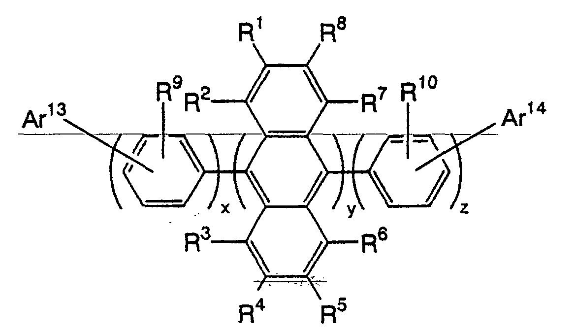
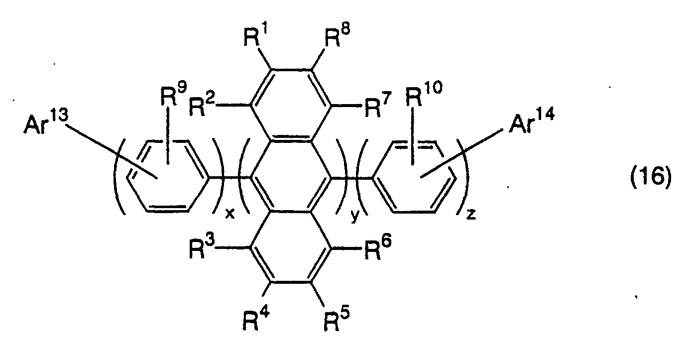
Suitable compounds with an anthracene nucleus
include compounds represented by the formula (16).
wherein R
1 to R
10 are independently a hydrogen atom, a
halogen atom, a substituted or unsubstituted C
1-20 alkyl
group, a substituted or unsubstituted C
1-20 alkoxy group, a
substituted or unsubstituted C
6-30 aryloxy group, a
substituted or unsubstituted C
1-20 alkylthio group, a
substituted or unsubstituted C
6-30 arylthio group, a
substituted or unsubstituted C
7-30arylalkyl group,a
unsubstituted C
5-30 monocyclic group, a substituted or
unsubstituted C
10-30 condensed polycyclic group, or a
substituted or unsubstituted C
5-30 heterocyclic group; Ar
13
and Ar
14 are independently a substituted or unsubstituted C
6-30
aryl group, the substituent of the aryl group is a
substituted or unsubstituted C
1-20 alkyl group, a substituted
or unsubstituted C
1-20 alkoxy group, a substituted or
unsubstituted C
6-30 aryloxy group, a substituted or
unsubstituted C
1-20 alkylthio group, a substituted or
unsubstituted C
6-30 arylthio group, a substituted or
unsubstituted C
7-30 arylalkyl group, a unsubstituted C
5-30
monocyclic group, a substituted or unsubstituted C
10-30
condensed polycyclic group, a substituted or unsubstituted
C
5-30 heterocyclic group, or a substituted or unsubstituted
C
4-40 alkenyl group; x and z are an integer of 0 to 3; and y
is an integer of 1 to 2.
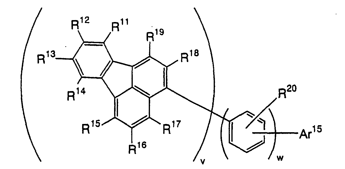
Suitable compounds with a fluoranthene nucleus
include compounds represented by the formula (17).
wherein R
11 to R
20 and Ar
15 are the same as R
1 to R
10 and Ar
13
and Ar
14 of the formula (16), respectively; and v and w are
an integer of 1 to 3.
The thickness of an electron injecting layer is not
limited. However, it is preferably 1 to 50 nm, more
preferably 2 to 30 nm, still more preferably 3 to 25 nm.
If the thickness is less than 1 nm, the property of
electron injection may not be improved, whereas if it is
more than 50 nm, the luminous efficiency of an organic EL
element may be decreased or the half life thereof may be
shortened.
(2) Organic Luminescent Layer
The aromatic amine compounds represented by the
formulas (3) arid (4) are used in an organic luminescent
layer. The reason for the use of the compounds with at
least three condensed aromatic rings is that excellent
luminance can be obtained at voltages as low as about 10 V
in cases where an electron injecting layer is provided.
Further, even in cases where the above aromatic
amine compounds contain a styryl or alkenyl group as a
substituent, if the above-mentioned hydrocarbon compounds
of certain structure are used in an electron injecting
layer, the half life is remarkably extended.
Materials, electron mobility, additives, methods of
formation and thickness of the organic luminescent layer in
the third embodiment are the same as those of the first
embodiment.
Examples
[Example 1]
(1) Formation of Organic EL Element
A transparent electrode with a thickness of 75 nm
was formed from indium tin oxide (ITO) as an anode layer on
a transparent glass substrate with a dimension of
thickness:1.1 mm × length:25 mm × width:75 mm. The
resultant substrate was ultrasonically washed in isopropyl
alcohol, dried in a nitrogen gas atmosphere, and washed for
10 minutes using W (ultraviolet radiation) and ozone.
Next, the substrate with the transparent electrode
was placed on a substrate holder in a deposition vessel of
a vacuum deposition device. After reducing the pressure in
the vacuum vessel to 1×10⁻³ Pa, a positive hole injecting
layer, an organic luminescent layer, an inorganic compound
layer and a cathode were sequentially laminated on the
anode layer to form an organic EL element under the
following deposition conditions.
Positive hole injecting layer:
4,4'-bis-(N1N-di-m-tolylamino)-4''-phenyl-triphenylamine
(TPD74)
Deposition rate: 0.2 nm/sec.
Thickness: 80 nm
Organic luminescent layer:
3,11-bis(diphenylamino)-7,14-diphenyl-acenaphtho(1,2-k)fluoranthene
(.Compound 8)
Deposition rate: 0.2 nm/sec.
Thickness: 50 nm
Inorganic compound layer:
LiF
Deposition rate: 0.2 nm/sec.
Thickness: 1 nm
Cathode layer:
Al
Deposition rate: .0.2 nm/sec.
Thickness: 200 nm
(2) Evaluation of Organic EL Element
A DC voltage of 6 V was applied between the cathode
layer and the anode layer of the organic EL element thus
obtained. The luminance was 540 cd/cm2 and the emitted
color was orange.
Furthermore, when the organic EL element was driven
at a constant current on condition that the initial
luminance was 500 cd/cm2, the half-life was 3,200 hours.
The results were shown in Table 1.
[Examples 2 to 6]
In Examples 2 to 6, organic EL elements were formed
in a manner similar to that of Example 1 except that the
compound 5 (Example 2), the compound 6 (Example 3), the
compound 9 (Example 4), the compound 10 (Example 5) and the
compound 1 (Example 6) were used instead of the compound 8
of Example 1. A DC voltage of 5.5 V or 6 V was applied
between a cathode layer and an anode layer for evaluation.
As a result, color of emitted light as shown in
Table 1 was observed, luminance was 310 to 720 cd/m2 and
half-life was 2,100 to 3,700 hours.
The results obtained were shown in Table 1.
| | Example 1 | Example 2 | Example 3 | Example 4 | Example 5 | Example 6 |
| positive hole injecting layer | TPD74 | TPD74 | TPD74 | TPD74 | TPD74 | TPD74 |
| luminescent material | compound 8 | compound 5 | compound 6 | compound 9 | compound 10 | compound 1 |
| inorganic compound layer | LiF | LiF | LiF | LiF | LiF | LiF |
| driving voltage(V) | 6 | 5.5 | 5.5 | 5.5 | 5.5 | 6 |
| color of emitted light | orange | green | green | orange | red orange | blue green |
| luminance (cd/m2) | 540 | 620 | 310 | 460 | 720 | 540 |
| half-life (hour) | 3,200 | 3,000 | 2,500 | 2,100 | 3,700 | 3,200 |
In Comparative Examples 1 to 3, organic EL elements
were formed in a manner similar to that of Example 1 except
that an electron transport layer with a thickness of 20 nm
was formed from tris(8-hydroxyquinolinate)aluminum (Alq)
instead of the inorganic compound layer of Example 1; and
the compound 1 (Comparative Example 1), the compound 6
(Comparative Example 2) and the compound 4 (Comparative
Example 3) were used as a luminescent material. A DC
voltage of 5.5 V was applied between a cathode layer and an
anode layer for evaluation.
As a result, color of emitted light as shown in
Table 2 was observed, luminance was 250 to 470 cd/m
2 and
half-life was 700 to 1,600 hours. The results obtained were
shown in Table 2.
| | Comparative Example 1 | Comparative Example 2 | Comparative Example 3 |
| positive hole injecting layer | TPD74 | TPD74 | TPD74 |
| luminescent material | compound 1 | compound 6 | compound 9 |
| electron injecting layer | Alq | Alq | Alq |
| driving voltage(V) | 5.5 | 5.5 | 5.5 |
| color of emitted light | orange | green | orange |
| luminance (cd/m2) | 470 | 250 | 320 |
| half-life (hour) | 1,600 | 1,300 | 700 |
In Example 7, a organic EL element was formed in a
manner similar to that of Example 1 except that an
interface layer (reductive dopant layer) with a thickness
of 20 nm was formed from a mixture of the compound 1 and
metal lithium (Li) as a reductive dopant (mixture mole
ratio 1:1) instead of the inorganic compound layer, by
using the compound 1 instead of the compound 8 of Example 1.
A DC voltage of 5.5 V was applied between a cathode layer
and an anode layer for evaluation.
As a result, orange light was observed, luminance
was 610 cd/m2 and half-life was 2,800 hours. The results
obtained were shown in Table 3.
[Example 8]
In Example 8, a organic EL element was formed in a
manner similar to that of Example 1 except that an
interface layer (reductive dopant layer) with a thickness
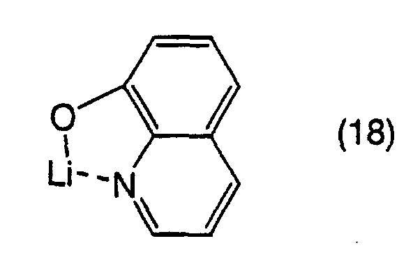
of 1 nm was formed at an interface area from a lithium
metal complex of the following formula (18) (hereinafter
referred to as a compound 11) as a reductive dopant instead
of the inorganic compound layer, by using the compound 1
instead of the compound 8 of Example 1. A DC voltage of 6.5
V was applied between a cathode layer and an anode layer
for evaluation.
As a result, blue green light was observed,
luminance was 530 cd/m
2 and half-life was 3,300 hours. The
results obtained were shown in Table 3.
In Example 9, a organic EL element was formed in a
manner similar to that of Example 8 except that an
interface layer (reductive dopant layer) with a thickness
of 1 nm was formed from a mono(2,2,6,6-tetramethyl-3,5-heptanedionate)lithium
complex (Li(dpm)) instead of the
reductive dopant of Example 8. A DC voltage of 6.5V was
applied between a cathode layer and an anode layer for
evaluation.
As a result, orange light was observed, luminance .
was 470 cd/m2 and half-life was 3,000 hours. The results
obtained were shown in Table 3.
[Example 10]
In Example 10, a organic EL element was formed in a
manner similar to that of Example 8 except that an
interface layer (reductive dopant layer) with a thickness
of 5 nm was formed from a mixture of the compound 1 and
Li(dpm) as a reductive dopant (mixture mole ratio 1:1)
instead of the reductive dopant of Example 8 as a
luminescent material. A DC voltage of 6.5 V was applied
between a cathode layer and an anode layer for evaluation.
As a result, orange light was observed, luminance
was 580 cd/m2 and half-life was 3,900 hours. The results
obtained were shown in Table 3.
[Example 11]
In Example 11, a organic EL element was formed in a
manner similar to that of Example 1 except that an electron
injecting layer with a thickness of 20 nm was formed from a
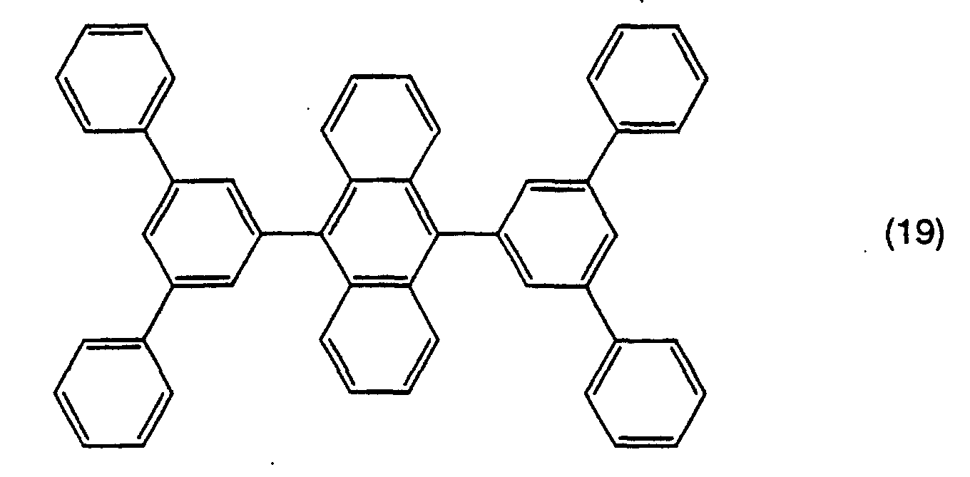
mixture of a phenylanthracene compound of the following
formula (19) (hereinafter referred to as a compound 12,
energy gap: 3.0 eV) and metal lithium (Li) as a reductive
dopant (mixture mole ratio 1:1) instead of the inorganic
compound layer of Example 1. A DC voltage of 6.5 V was
applied between a cathode layer and an anode layer for
evaluation.
As a result, blue green light was observed,
luminance was 430 cd/m
2 and half-life was 2,600 hours. The
results obtained were shown in Table 3.
In Example 12, a organic EL element was formed in a
manner similar to that of Example 1 except that the
compound 1 was used instead of the compound 8 of Example 1,
and an electron injecting layer with a thickness of 20 nm
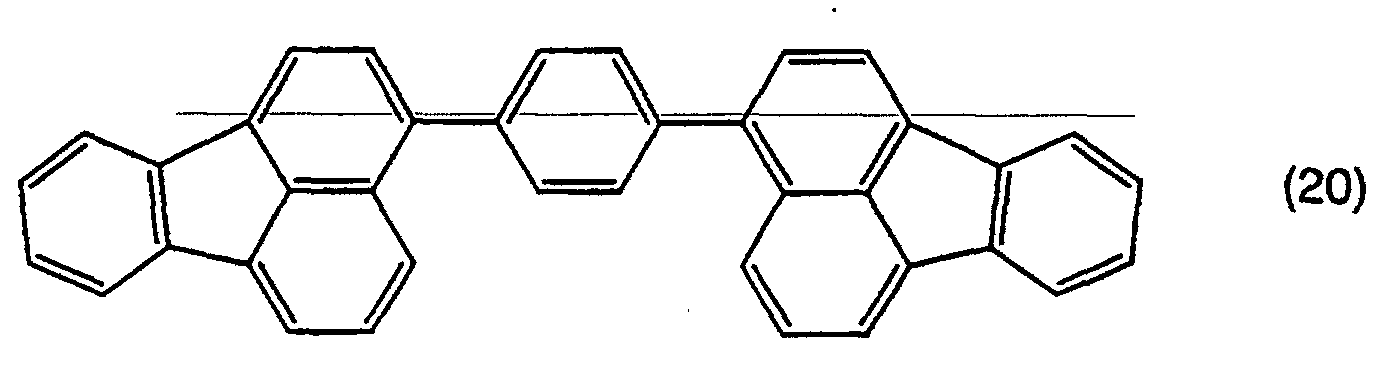
was formed from a mixture of a fluoranthene compound of the
following formula (20) (hereinafter referred to as a
compound 13, energy gap: 2.8 eV) and metal lithium (Li) as
a reductive dopant (mixture mole ratio 1:1) instead of the
inorganic compound layer of Example 1. A DC voltage of 6.5
V was applied between a cathode layer and an anode layer
for evaluation.
As a result, blue green light was observed,
luminance was 530 cd/m
2 and half-life was 3,800 hours. The
results obtained were shown in Table 3.
| | Example 7 | Example 8 | Example 9 | Example 10 | Example 11 | Example 12 |
| positive hole injecting layer | TPD74 | TPD74 | TPD74 | TPD74 | TPD74 | TPD74 |
| luminescent material | compound 8 | compound 1 | compound 8 | compound 8 | compound 1 | compound 1 |
| interface layer | compound 1/Li | compound 11 | Li(dpm) | compound 1/Li(dpm) |
| electron injecting layer | | | | | compound | 12/Li | compound 13/Li |
| driving voltage(v) | 5.5 | 6.5 | 6.5 | 6.5 | 6.5 | 6.5 |
| color of emitted light | orange | blue green | orange | orange | blue green | blue green |
| luminance (cd/m2) | 540 | 530 | 470 | 580 | 430 | 530 |
| half-life (hour) | 3,200 | 3,300 | 3,000 | 3,900 | 2,600 | 3,800 |
As described in detail above, according to the
first aspect of the invention, even in cases where an
electron injecting layer made of an inorganic compound is
provided, by using an aromatic amine compound containing at
least three condensed aromatic rings as a luminescent
material, electrons can effectively combine positive holes
in an organic luminescent layer. Consequently, there could
be provided an organic EL element with higher luminance,
e.g., 500 cd/m2 or more even at low driving voltages and
estremely longer half-life, e.g., more than 2,000 hours.
According to the second aspect of the invention, by
arranging a reductive dopant layer and further using an
aromatic amine compound containing at least three condensed
aromatic rings in an organic luminescent layer, there could
be similarly provided an organic EL element with higher
luminance even at low driving voltages and extremely longer
half-life.
According to the third aspect of the invention, by
using a certain hydrocarbon compound in an electron
injecting layer and further using an aromatic amine
compound containing at least three condensed aromatic rings
in an organic luminescent layer, there could be similarly
provided an organic EL element with higher luminance even
at low driving voltages and extremely longer half-life.


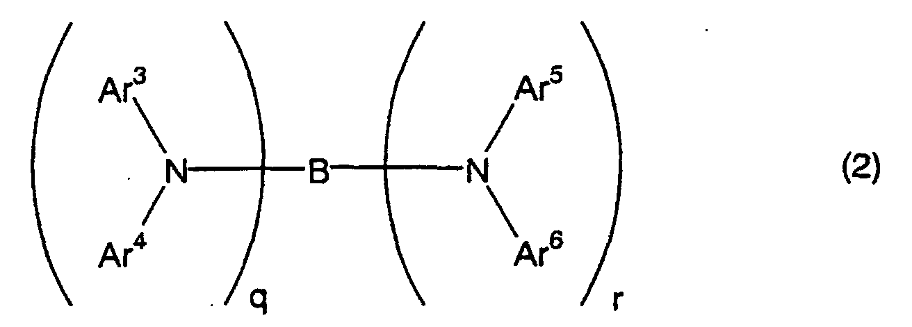







 wherein B, Ar3, Ar4, Ar5 and Ar6 are independently a substituted or unsubstituted C6-60 aromatic group which does not contain a styryl group nor an alkenyl group, at least one of B, Ar3, Ar4, Ar5 and Ar6 contains substituted or unsubstituted at least three condensed aromatic rings, and q and r of a condensation number are an integer of 1 to 6.
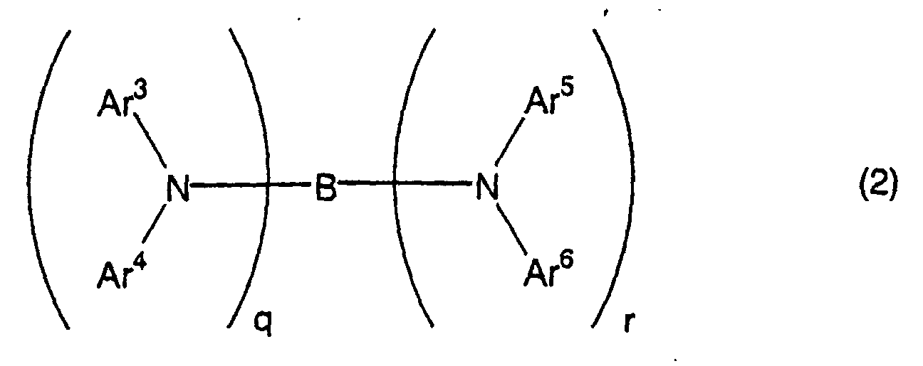
 wherein B, Ar3, Ar4, Ar5 and Ar6 are independently a substituted or unsubstituted C6-60 aromatic group which does not contain a styryl group nor an alkenyl group, at least one of B, Ar3, Ar4, Ar5 and Ar6 contains substituted or unsubstituted at least three condensed aromatic rings, and q and r of a condensation number are an integer of 1 to 6.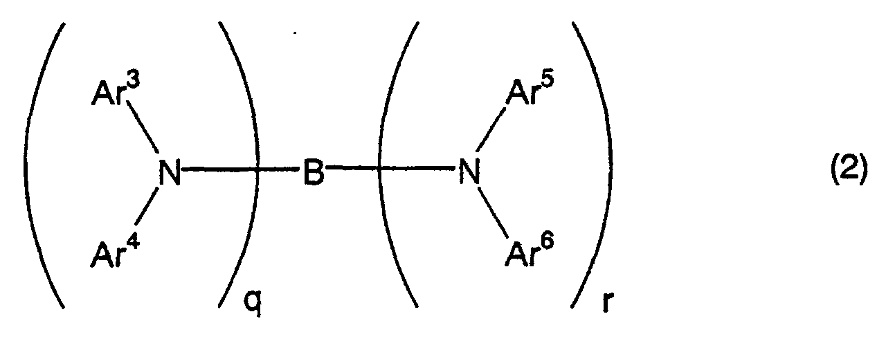
 wherein B, Ar9, Ar10, Ar11 and Ar12 are independently a substituted or unsubstituted C6-60 aromatic group, at least one of B, Ar9, Ar10, Ar11 and Ar12 contains substituted or unsubstituted at least three condensed aromatic rings, and q and r of a condensation number are an integer of 1 to 6.