EP1345258A2 - Semiconductor device and method of manufacturing the same - Google Patents
Semiconductor device and method of manufacturing the same Download PDFInfo
- Publication number
- EP1345258A2 EP1345258A2 EP03250684A EP03250684A EP1345258A2 EP 1345258 A2 EP1345258 A2 EP 1345258A2 EP 03250684 A EP03250684 A EP 03250684A EP 03250684 A EP03250684 A EP 03250684A EP 1345258 A2 EP1345258 A2 EP 1345258A2
- Authority
- EP
- European Patent Office
- Prior art keywords
- film
- etching
- hard mask
- semiconductor device
- conductive
- Prior art date
- Legal status (The legal status is an assumption and is not a legal conclusion. Google has not performed a legal analysis and makes no representation as to the accuracy of the status listed.)
- Granted
Links
Images






Classifications
-
- H—ELECTRICITY
- H10—SEMICONDUCTOR DEVICES; ELECTRIC SOLID-STATE DEVICES NOT OTHERWISE PROVIDED FOR
- H10B—ELECTRONIC MEMORY DEVICES
- H10B53/00—Ferroelectric RAM [FeRAM] devices comprising ferroelectric memory capacitors
-
- H—ELECTRICITY
- H10—SEMICONDUCTOR DEVICES; ELECTRIC SOLID-STATE DEVICES NOT OTHERWISE PROVIDED FOR
- H10D—INORGANIC ELECTRIC SEMICONDUCTOR DEVICES
- H10D84/00—Integrated devices formed in or on semiconductor substrates that comprise only semiconducting layers, e.g. on Si wafers or on GaAs-on-Si wafers
-
- H—ELECTRICITY
- H10—SEMICONDUCTOR DEVICES; ELECTRIC SOLID-STATE DEVICES NOT OTHERWISE PROVIDED FOR
- H10B—ELECTRONIC MEMORY DEVICES
- H10B53/00—Ferroelectric RAM [FeRAM] devices comprising ferroelectric memory capacitors
- H10B53/30—Ferroelectric RAM [FeRAM] devices comprising ferroelectric memory capacitors characterised by the memory core region
-
- H—ELECTRICITY
- H10—SEMICONDUCTOR DEVICES; ELECTRIC SOLID-STATE DEVICES NOT OTHERWISE PROVIDED FOR
- H10D—INORGANIC ELECTRIC SEMICONDUCTOR DEVICES
- H10D1/00—Resistors, capacitors or inductors
- H10D1/60—Capacitors
- H10D1/68—Capacitors having no potential barriers
- H10D1/682—Capacitors having no potential barriers having dielectrics comprising perovskite structures
-
- H—ELECTRICITY
- H10—SEMICONDUCTOR DEVICES; ELECTRIC SOLID-STATE DEVICES NOT OTHERWISE PROVIDED FOR
- H10P—GENERIC PROCESSES OR APPARATUS FOR THE MANUFACTURE OR TREATMENT OF DEVICES COVERED BY CLASS H10
- H10P50/00—Etching of wafers, substrates or parts of devices
- H10P50/20—Dry etching; Plasma etching; Reactive-ion etching
- H10P50/26—Dry etching; Plasma etching; Reactive-ion etching of conductive or resistive materials
- H10P50/264—Dry etching; Plasma etching; Reactive-ion etching of conductive or resistive materials by chemical means
- H10P50/266—Dry etching; Plasma etching; Reactive-ion etching of conductive or resistive materials by chemical means by vapour etching only
- H10P50/267—Dry etching; Plasma etching; Reactive-ion etching of conductive or resistive materials by chemical means by vapour etching only using plasmas
-
- H—ELECTRICITY
- H10—SEMICONDUCTOR DEVICES; ELECTRIC SOLID-STATE DEVICES NOT OTHERWISE PROVIDED FOR
- H10P—GENERIC PROCESSES OR APPARATUS FOR THE MANUFACTURE OR TREATMENT OF DEVICES COVERED BY CLASS H10
- H10P50/00—Etching of wafers, substrates or parts of devices
- H10P50/20—Dry etching; Plasma etching; Reactive-ion etching
- H10P50/28—Dry etching; Plasma etching; Reactive-ion etching of insulating materials
- H10P50/282—Dry etching; Plasma etching; Reactive-ion etching of insulating materials of inorganic materials
- H10P50/283—Dry etching; Plasma etching; Reactive-ion etching of insulating materials of inorganic materials by chemical means
- H10P50/285—Dry etching; Plasma etching; Reactive-ion etching of insulating materials of inorganic materials by chemical means of materials not containing Si, e.g. PZT or Al2O3
-
- H—ELECTRICITY
- H10—SEMICONDUCTOR DEVICES; ELECTRIC SOLID-STATE DEVICES NOT OTHERWISE PROVIDED FOR
- H10P—GENERIC PROCESSES OR APPARATUS FOR THE MANUFACTURE OR TREATMENT OF DEVICES COVERED BY CLASS H10
- H10P50/00—Etching of wafers, substrates or parts of devices
- H10P50/71—Etching of wafers, substrates or parts of devices using masks for conductive or resistive materials
-
- H—ELECTRICITY
- H10—SEMICONDUCTOR DEVICES; ELECTRIC SOLID-STATE DEVICES NOT OTHERWISE PROVIDED FOR
- H10P—GENERIC PROCESSES OR APPARATUS FOR THE MANUFACTURE OR TREATMENT OF DEVICES COVERED BY CLASS H10
- H10P50/00—Etching of wafers, substrates or parts of devices
- H10P50/73—Etching of wafers, substrates or parts of devices using masks for insulating materials
-
- H—ELECTRICITY
- H10—SEMICONDUCTOR DEVICES; ELECTRIC SOLID-STATE DEVICES NOT OTHERWISE PROVIDED FOR
- H10B—ELECTRONIC MEMORY DEVICES
- H10B12/00—Dynamic random access memory [DRAM] devices
- H10B12/30—DRAM devices comprising one-transistor - one-capacitor [1T-1C] memory cells
- H10B12/31—DRAM devices comprising one-transistor - one-capacitor [1T-1C] memory cells having a storage electrode stacked over the transistor
- H10B12/312—DRAM devices comprising one-transistor - one-capacitor [1T-1C] memory cells having a storage electrode stacked over the transistor with a bit line higher than the capacitor
Definitions
- the present invention relates to a semiconductor device and a method of manufacturing the same and, more particularly, a semiconductor device having capacitors over a semiconductor substrate and a method of manufacturing the same.
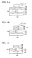
- the ferroelectric capacitor is formed by the steps described in the following.
- the first metal layer 106, the PZT layer 107, and the second metal layer 108 are formed sequentially on the interlayer insulating film 104 for covering the semiconductor substrate 101.
- the impurity diffusion region 103 surrounded by the element isolation insulating film 102 is formed on the semiconductor substrate 101, and the conductive plug 105 is formed in the interlayer insulating film 104 on the impurity diffusion region 103.
- the titanium nitride layer 110 and the silicon oxide layer 111 are formed sequentially on the second metal layer 108. Then, the silicon oxide layer 111 and the titanium nitride layer 110 are patterned by the photolithography method to be left over the conductive plug 105 as the hard mask 112 having the capacitor planar shape.
- the second metal layer 108, the PZT layer 107, and the first metal layer 106 in the region, which is not covered with the hard mask 112, are etched sequentially.
- the stacked ferroelectric capacitor 113 is formed on the interlayer insulating film 104.
- the silicon oxide layer 111 constituting the hard mask 112 is removed, and then the titanium nitride layer 110 is removed by changing the etchant.
- the reason why not a resist mask but the hard mask 112 is employed to pattern the first metal layer 106, the PZT layer 107, and the second metal layer 108 is given as follows.
- the first metal layer 106, the PZT layer 107, and the second metal layer 108 are etched successively by using a resist mask, such a resist mask disappears during the etching since the resist mask has a poor etching selectivity against these layers 106, 107, 108.
- the silicon oxide layer should be employed as the hard mask in patterning the PZT layer that is put between the first and second metal layers.
- the disappearance of the silicon oxide layer serving as the hard mask during the etching of the PZT layer causes a remarkable reduction in the etching rate of the PZT layer. Therefore, it is important to leave the silicon oxide layer 111 as the hard mask until the etching of the PZT layer is ended.
- the silicon oxide layer 111 and the titanium nitride layer 110 are removed by etching after the formation of the capacitor 113 is completed.
- the interlayer insulating film 104 formed of the silicon oxide is also etched around the capacitor 113.
- the level difference between the capacitor 113 and the periphery area is increased. If such a level difference is increased, such a disadvantage is caused that the filling property of the second-layer interlayer insulating film between plural capacitors 113 becomes worse.
- a semiconductor device comprising an insulating film formed over a semiconductor substrate; capacitor lower electrodes formed on the insulating film and having discontinuous steps on side surfaces; capacitor dielectric films formed on the capacitor lower electrodes and having side surfaces that continue to upper side surfaces of the capacitor lower electrodes; and capacitor upper electrodes formed on the capacitor dielectric films and having side surfaces that continue to the side surfaces of the capacitor dielectric films.
- a semiconductor device manufacturing method which comprises the steps of forming an insulating film over a semiconductor substrate; forming sequentially a first conductive film, a dielectric film, and a second conductive film on the insulating film; forming a first film made of metal or metal compound on the second conductive film; forming a second film made of insulating material on the first film; forming hard masks by patterning the second film and the first film into a capacitor planar shape; forming capacitor upper electrodes by etching the second conductive film in a region that is not covered with the hard masks; forming capacitor dielectric films by etching the dielectric film in the region that is not covered with the hard masks; etching the first conductive film in the region that is not covered with the hard masks up to a depth that does not expose the insulating film; removing the second film constituting the hard masks by etching; forming capacitor lower electrodes by etching a remaining portion of the first conductive
- a semiconductor device manufacturing method which comprises the steps of forming an insulating film over a semiconductor substrate; forming sequentially a first conductive film, a dielectric film, and a second conductive film on the insulating film; forming a first film made of metal or metal compound on the second conductive film; forming a second film made of a silicon nitride film, which is different material from the insulating film, on the first film; forming hard masks by patterning the second film and the first film into a capacitor planar shape; forming capacitor upper electrodes by etching the second conductive film in a region that is not covered with the hard masks; forming capacitor dielectric films by etching the dielectric film in the region that is not covered with the hard masks; forming capacitor lower electrodes by etching the first conductive film in the region that is not covered with the hard masks; removing the second film constituting the hard masks by etching using an etching gas containing flu
- an insulating material is employed as the uppermost layer of the hard mask that is used to pattern the first conductive film, the dielectric film, and the second conductive film formed on the insulating film. Then, removal of the uppermost layer is executed by interrupting the etching of the first conductive film, and then the etching of the first conductive film is started once again.
- the underlying insulating film is never exposed.
- the etching of the underlying insulating film of the capacitor can be suppressed.
- the deposition products that adhere onto the side walls of the hard mask by the etching of the dielectric film can be removed by the etching of the first conductive film applied before the uppermost layer of the hard mask is removed.
- removal of the uppermost layer of the hard mask can be facilitated.
- stepped portions are generated on side surfaces of the capacitor lower electrodes that are formed by patterning the first conductive film.
- the uppermost layer of the hard mask is formed of silicon nitride, and then the capacitor is formed by etching the first conductive film, the dielectric film, and the second conductive film continuously while using this hard mask.
- the uppermost insulating layer constituting the hard mask can be easily etched selectively to the insulating film after the capacitor is formed.
- the etching of the underlying insulating film of the capacitor can be suppressed.
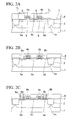
- FIGS. 2A to 2M are sectional views showing steps of manufacturing a semiconductor device according to a first embodiment of the present invention.
- an element isolation recess is formed around a transistor forming region of an n-type or p-type silicon (semiconductor) substrate 1 by the photolithography method. Then, an element isolation insulating film 2 is formed by burying silicon oxide (SiO 2 ) into the element isolation recess.
- the element isolation insulating film 2 having such a structure is called STI (Shallow Trench Isolation).
- an insulating film formed by the LOCOS (Local Oxidation of Silicon) method may be employed as the element isolation insulating film.
- a p-well 1a is formed by introducing a p-type impurity into the transistor forming region of the silicon substrate 1.
- a silicon oxide film as a gate insulating film 3 is formed by oxidizing thermally a surface of the transistor forming region of the silicon substrate 1.
- gate electrodes 4a, 4b are formed by patterning the silicon film and the tungsten silicide film by virtue of the photolithography method.
- gate electrodes 4a, 4b are formed in parallel on one p-well 1a. These gate electrodes 4a, 4b constitute a part of the word line.
- first to third n-type impurity diffusion regions 5a to 5c serving as the source/drain are formed by ion-implanting an n-type impurity into the p-well 1a on both sides of the gate electrodes 4a, 4b.
- an insulating film e.g., a silicon oxide (SiO 2 ) film, is formed on an overall surface of the silicon substrate 1 by the CVD method. Then, insulating sidewall spacers 6 are left on both side portions of the gate electrodes 4a, 4b by etching back the insulating film.
- a silicon oxide (SiO 2 ) film is formed on an overall surface of the silicon substrate 1 by the CVD method. Then, insulating sidewall spacers 6 are left on both side portions of the gate electrodes 4a, 4b by etching back the insulating film.
- the n-type impurity is ion-implanted into the first to third n-type impurity diffusion regions 5a to 5c once again by using the gate electrodes 4a, 4b and the sidewall spacers 6 as a mask.
- the first to third n-type impurity diffusion regions 5a to 5c are formed into the LDD structure.
- the first and second n-type impurity diffusion regions 5a, 5b positioned on both end sides of one p-well 1a are connected electrically to the lower electrodes of the capacitors, and the third n-type impurity diffusion region 5c positioned between two gate electrodes 4a, 4b is connected electrically to the bit line.
- two MOS transistors T 1 , T 2 having the gate electrodes 4a, 4b and the n-type impurity diffusion regions 5a to 5c having the LDD structure are formed in the p-well 1a.
- a silicon oxide nitride (SiON) film of about 200 nm thickness is formed as a cover insulating film 7, which covers the MOS transistors T 1, T 2 , on an overall surface of the silicon substrate 1 by the plasma CVD method.
- a silicon oxide (SiO 2 ) film of about 1.0 ⁇ m is formed as a first interlayer insulating film 8 on the cover insulating film 7 by the plasma CVD method using the TEOS gas.
- the first interlayer insulating film 8 is annealed in a normal-pressure nitrogen atmosphere at a temperature of 700°C for 30 minutes, for example. Then, an upper surface of the first interlayer insulating film 8 is planarized by the CMP (Chemical Mechanical Polishing) method.
- CMP Chemical Mechanical Polishing
- first and second contact holes 8a, 8b that have a depth to reach the first and second n-type impurity diffusion regions 5a, 5b, respectively, are formed by patterning the first interlayer insulating film 8 and the cover insulating film 7 by virtue of the photolithography method.
- a titanium (Ti) film of about 30 nm thickness and a titanium nitride (TiN) film of about 50 nm thickness are formed sequentially as a glue film on an upper surface of the first interlayer insulating film 8 and inner surfaces of the first and second contact holes 8a, 8b by the sputter method.
- a tungsten (W) film is grown on the TiN film by the CVD method using WF 6 to bury completely insides of the first and second contact holes 8a, 8b.
- the W film, the TiN film, and the Ti film are polished by the CMP method to remove them from the upper surface of the first interlayer insulating film 8.
- the W film, the TiN film, and the Ti film being left in the first and second contact holes 8a, 8b are used as first and second conductive plugs 9a, 9b.
- an iridium (Ir) film 15x of about 200 nm thickness, an iridium oxide (IrO x ) film 15y of about 50 nm thickness, and a platinum (Pt) film 15z of about 100 nm thickness, for example, are formed sequentially as a first conductive film 15 on the first and second conductive plugs 9a, 9b and the first interlayer insulating film 8 by the sputter.
- the first conductive film 15 may be formed of a conductive film containing other platinum-group metal or platinum-group metal oxide.
- the first interlayer insulating film 8 is annealed to prevent the film peeling-off, for example, before or after the first conductive film 15 is formed.
- annealing method RTA (Rapid Thermal Annealing) executed in an argon atmosphere at 600 to 750°C, is employed.
- the method of forming the ferroelectric film 16 in addition to this, there are the MOD (Metal Organic Deposition) method, the MOCVD (Metal Organic CVD) method, the sol-gel method, etc.
- the material of the ferroelectric film 16 in addition to PZT in addition to PZT, other PZT material such as PLCSZT, PLZT, etc., the Bi layered-structure compound material such as SrBi 2 Ta 2 O 9 , SrBi 2 (Ta,Nb) 2 O 9 , etc., other metal oxide ferroelectric substance, etc. may be employed.
- the ferroelectric film 16 is crystallized by executing annealing in an oxygen atmosphere.
- a two-step RTA process having the first step in which the annealing is executed in a mixed-gas atmosphere consisting of argon and oxygen at a substrate temperature of 600°C for 90 seconds, and the second step in which the annealing is executed in an oxygen atmosphere at a substrate temperature of 750°C for 60 seconds, for example, is employed.
- IrO 2 iridium oxide
- a TiN film 18a and a SiO 2 film (insulating film) 18b serving as a hard mask are formed sequentially on the second conductive film 17.
- the TiN film 18a is formed by the sputter method to have a thickness of about 200 nm, for example.
- the SiO 2 film 18b is formed by the plasma CVD method using TEOS (tetraethoxysilane) to have a thickness of about 800 nm, for example.
- resist R is coated on the SiO 2 film 18b, and then patterns are formed by exposing/developing this resist to have a capacitor planar shape over the first and second conductive plugs 9a, 9b respectively.
- the SiO 2 film 18b formed in the region that is not covered with the resist R is removed by dry etching using C 4 F 8 , Ar, and CF 4 as the etching gas.
- the TiN film 18a formed in the region that is not covered with the resist R is removed by dry etching using BCl 3 and Cl 2 as the etching gas.
- the etching of the SiO 2 film 18b and the etching of the TiN film 18a are carried out by changing the etchant.
- the SiO 2 film 18b and the TiN film 18a, after patterned, are used as the hard mask 18.
- the resist R is removed by ashing.
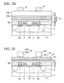
- the second conductive film 17, the ferroelectric film 16, and the first conductive film 15 formed in the region that is not covered with the hard mask 18 are etched sequentially under the following conditions by using the ICP etching equipment.
- the IrO x film as the second conductive film 17 is etched.
- HBr and O 2 are supplied to the etching chamber at a flow rate of 10 sccm and a flow rate of 40 sccm respectively, the pressure in the chamber is set to 0.4 Pa, the wafer stage temperature is set to 400°C the source power is set to 800 watt, and the bias power is set to 700 watt.
- the source power is the power of the high-frequency power supply applied to the antenna of the ICP etching equipment, and the bias power is the power of the high-frequency power supply applied to the semiconductor wafer (silicon substrate 1).
- the etching of the second conductive film 17 is detected by using the end-point detector, and the over-etching is executed by about 10 % of the film thickness of the second conductive film 17.
- an emission spectrophotometer is employed as the end-point detector, for example.
- the PZT film as the ferroelectric film 16 is etched.
- Cl 2 and Ar are supplied to the etching chamber at a flow rate of 40 sccm and a flow rate of 10 sccm respectively, the pressure in the chamber is set to 0.4 Pa, the wafer stage temperature is set to 400°C, the source power is set to 800 watt, and the bias power is set to 700 watt.
- the etching of the ferroelectric film 16 is detected by using the end-point detector, and the just-etching is executed.
- the SiO 2 film 18b constituting the hard mask 18 should be removed.
- the products generated during the etching of the first conductive film 15 and the ferroelectric film 16 are deposited onto side surfaces of the SiO 2 film 18b as the noble metal deposition film, it is difficult to remove the SiO 2 film 18b as it is.
- the ferroelectric film 16 is etched while the SiO 2 film 18b as the upper layer portion of the hard mask 18 is still left, and subsequently the first conductive film 15 of the multi-layered structure is under-etched in the middle.
- This under-etching is the half- etching that is carried out until about 50 % of the film thickness, for example.
- the under-etching is carried out up to the middle of the etching process of the first conductive film 15. For example, this under-etching is carried out up to a depth that reaches the upper portion of the Ir film 15x after the etchings of the Pt film 15z and the IrO x 15y are ended.
- HBr and O 2 are supplied to the etching chamber at a flow rate of 10 sccm and a flow rate of 40 sccm respectively, the pressure in the chamber is set to 0.4 Pa, the wafer stage temperature is set to 400°C, the source power is set to 800 watt, and the bias power is set to 700 watt.
- the noble metal deposition film is removed from side surfaces of the SiO 2 film 18b.
- the silicon substrate 1 is taken out from the ICP etching equipment and then put into the plasma etching equipment. Then, as shown in FIG.2G, in the state that the silicon substrate 1 is cooled, the SiO 2 film 18b of the hard mask 18 is removed by etching using a mixed gas consisting of CF 4 , CHF 3 , and Ar.
- a polymer deposited product is produced at the time of the etching of the SiO 2 film 18b. This polymer deposited product remains on side surfaces of respective layers from the hard mask 18 to the first conductive film 15. If the polymer deposited product is formed thick, such deposited product functions as the etching mask. Therefore, such polymer deposited product is removed by using ashing equipment using oxygen-containing gas.
- the silicon substrate 1 is put back into the ICP etching equipment.
- the etching of the first conductive film 15 is restarted by using the hard mask 18 that has a single-layer structure of the TiN film 18a.
- the etching conditions in this case are set identically to the etching conditions for the upper portion of the first conductive film 15, and the remaining portion of the first conductive film 15 is etched for a predetermined time. Accordingly, an upper surface of the first interlayer insulating film 8 is exposed.
- each of the capacitors Q has a lower electrode 15a made of the first conductive film 15, a dielectric film 16a made of the ferroelectric film 16, and an upper electrode 17a made of the second conductive film 17.
- the lower electrodes 15a of the capacitors Q are connected to the first and second n-type impurity diffusion regions 5a, 5b via the first and second conductive plugs 9a, 9b respectively.
- the TiN film 18a being left as the hard mask 18 is removed.
- isotropic etching should be employed to enhance the etching selectivity to SiO 2 constituting the first interlayer insulating film 8.
- a dry process employing down-flow etching using an etching gas containing CF 4 and O 2 , or a wet process using a mixed solution of NH 4 OH, H 2 O 2 , and H 2 O is effective.
- the selective etching of the TiN film 18a to the 3102 film can be executed.
- the first interlayer insulating film 8 around the capacitors Q is seldom etched and therefore no large recess is generated around the capacitors Q.
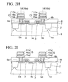
- recovery annealing of the capacitors Q is carried out.
- the recovery annealing in this case is carried out in an oxygen atmosphere at a substrate temperature of 650°C for 60 minutes, for example.
- an alumina film of 50 nm thickness is formed as a capacitor protection film 19 on surfaces of the capacitors Q and an underlying insulating film 10b by the sputter. Then, the capacitors Q are annealed in an oxygen atmosphere at 650°C for 60 minutes. The capacitor protection film 19 is formed to protect the capacitors Q from the process damage.
- a silicon oxide (SiO 2 ) film of about 1.0 ⁇ m thickness is formed as a second interlayer insulating film 20 on the capacitor protection film 19 by the plasma CVD method using the TEOS gas. Then, an upper surface of the second interlayer insulating film 20 is made flat by the CMP method. In this example, a remaining thickness of the second interlayer insulating film 20 after the CMP is set to about 300 nm on the upper electrode 17a of the capacitor Q.
- the second interlayer insulating film 20, the capacitor protection film 19, the first interlayer insulating film 8, and the cover insulating film 7 are etched by using a resist mask (not shown).
- a third contact hole 20a is formed on the third n-type impurity diffusion region 5c.
- a Ti film of 30 nm and a TiN film of 50 nm thickness are formed in order as a glue film in the third contact hole 20a and on the second interlayer insulating film 20 by the sputter method.
- a W film is grown on the glue film by the CVD method to bury completely the third contact hole 20a.
- the W film and the TiN film are polished by the CMP method to remove them from an upper surface of the second interlayer insulating film 20. Then, the tungsten film and the glue film being left in the third contact hole 20a are used as a third conductive plug 21.
- an SiON film is formed as an oxidation preventing film (not shown) on the third conductive plug 21 and the second interlayer insulating film 20 by the CVD method.
- contact holes 20b are formed on the upper electrodes 17a of the capacitors Q by patterning the oxidation preventing film and the second interlayer insulating film 20 by means of the photolithography method.
- the capacitors Q that are subjected to damage in forming the contact holes 20b can be recovered by annealing.
- the annealing is carried out in an oxygen atmosphere at a substrate temperature of 550 °C for 60 minutes, for example.
- the oxidation preventing film formed on the second interlayer insulating film 20 is removed by etching-back to expose a surface of the third conductive plug 21.
- a multi-layered metal film is formed in the contact holes 20b formed on the upper electrodes 17a of the capacitors Q and on the second interlayer insulating film 20.
- first-layer metal wirings 22a which are connected to the upper electrodes 17a via the contact holes 20b, and a conductive pad 22b, which is connected to the third conductive plug 21, are formed by patterning the multi-layered metal film.
- the multi-layered metal film a structure in which a Ti film of 60 nm thickness, a TiN film of 30 nm thickness, an Al-Cu film of 400 nm thickness, a Ti film of 5 nm thickness, and a TiN film of 70 nm thickness are formed sequentially, for example, is employed.
- the method of patterning the multi- layered metal film the method of forming a reflection preventing film (not shown) on the multi-layered metal film, then coating a resist (not shown) on the reflection preventing film, then forming resist patterns such as the wiring shape, etc. by exposing/developing the resist, and then etching the reflection preventing film and the multi- layered metal film by using the resist patterns is employed.
- a third interlayer insulating film 23 is formed on the second interlayer insulating film 20, the first-layer metal wirings 22a, and the conductive pad 22b. Then, a hole 23a is formed on the conductive pad 22b by patterning the third interlayer insulating film 23, and a fourth conductive plug 24 that consists of a TiN film and a W film sequentially from the bottom is formed in the hole 23a.
- second-layer wirings containing the bit line are formed on the third interlayer insulating film 23.
- the bit line is connected electrically to the third n-type impurity diffusion region 5c via the fourth conductive plug 24, the conductive pad 22b, and the third conductive plug 21.
- an insulating film for covering the second-layer wirings, etc. are formed, but their details will be omitted herein.
- the hard mask having the multi-layered structure is employed and also the SiO 2 film 18b is used as the uppermost layer. Then, the removal of the SiO 2 film 18b that is necessary for the etching of the ferroelectric film 16 is executed after the etching of the first conductive film 15 is temporarily interrupted.
- the first interlayer insulating film 8 is protected by the first conductive film 15 from the etching.
- the first conductive film 15 which is etched finally by using the hard mask 18, is formed of the platinum-group metal or the platinum-group oxide, the first conductive film 15 can be etched selectively to the silicon compound insulating material constituting the first interlayer insulating film 8.
- the interruption timing of the etching of the first conductive film 15 is not limited to about 50 % of the film thickness. However, it is preferable that the first conductive film 15 should be left to such extent that the first interlayer insulating film 8 is not exposed.
- a film thickness of the SiO 2 film 18b should be adjusted such that the SiO 2 film 18b can be removed at a point of time when the etching of the first conductive film 15 is ended.
- the etching of the SiO 2 film 18b proceeds easily at the edge portion rather than the center portion, and thus it is difficult to adjust such film thickness.
- the surface of the first interlayer insulating film 8 is composed of silicon nitride.
- the film quality of the lower electrodes 15a of the capacitors Q is deteriorated, and thus there is caused another disadvantage such that the crystal of the ferroelectric film 16 is deteriorated.
- the third contact hole 20a in which the third conductive plug 21 is buried is formed by etching the second interlayer insulating film 20 and the first interlayer insulating film 8 together.
- Such third contact hole 20a may be formed at two stages, as will be explained in a second embodiment.
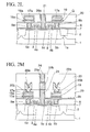
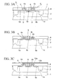
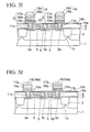
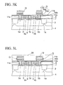
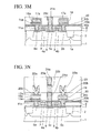
- FIGS.3A to 3N are sectional views showing steps of manufacturing a semiconductor device according to a second embodiment of the present invention.
- the element isolation insulating film 2 is formed on the silicon substrate 1,. then the p-well 1a is formed, then the MOS transistors T 1 , T 2 are formed, then the cover insulating film 7 and the first interlayer insulating film 8 are formed, then the densifying process of the first interlayer insulating film 8 is carried out, and the upper surface of the first interlayer insulating film 8 is made flat by the CMP method.
- a bit-line contact hole 8c having a depth to reach the third n-type impurity diffusion region 5c is formed by patterning the first interlayer insulating film 8 and the cover insulating film 7 by means of the photolithography method. Then, a Ti film of 30 nm thickness and a TiN film of 50 nm thickness are formed sequentially as a glue film on the upper surface of the first interlayer insulating film 8 and an inner surface of the bit-line contact hole 8c by the sputter method. Then, a W film is grown on the TiN film by the CVD method using WF6 to bury perfectly an interior of the bit-line contact hole 8c.
- the W film, the TiN film, and the Ti film are polished by the CMP method to remove them from the upper surface of the first interlayer insulating film 8.
- the W film, the TiN film, and the Ti film being left in the bit-line contact hole 8c is used as a first bit-line conductive plug 9.
- an oxidation-prevention insulating film 10a made of Si 3 N 4 of 100 nm thickness and the underlying insulating film 10b made of SiO 2 of 100 nm thickness are formed sequentially on the first interlayer insulating film 8 and the first bit-line conductive plug 9 by the plasma CVD method.
- the SiO 2 film is grown by the plasma CVD method using TEOS.
- the oxidation-prevention insulating film 10a is formed to prevent the event that, in the heat treatment such as the later annealing, or the like, the abnormal oxidation of the first bit-line conductive plug 9 is caused to thus generate contact failure. It is preferable that the film thickness should be set to more than 70 nm, for example.
- the oxidation-prevention insulating film 10a, the underlying insulating film 10b, the first interlayer insulating film 8, and the cover insulating film 7 are etched by using a resist pattern (not shown).
- the first and second contact holes 8a, 8b for the capacitor connection are formed on the first and second n-type impurity diffusion regions 5a, 5b respectively.
- a Ti film of 30 nm thickness and a TiN film of 50 nm thickness are formed sequentially as the glue film on the upper surface of the underlying insulating film 10b and the inner surfaces of the first and second contact holes 8a, 8b by the sputter method.
- a W film is grown on the TiN film by the CVD method to bury completely the inside of the first and second contact holes 8a, 8b.
- the W film, the TiN film, and the Ti film are polished by the CMP method to remove them from the upper surface of the underlying insulating film 10b.
- the W film, the TiN film, and the Ti film being left in the first and second contact holes 8a, 8b are used as first and second conductive plugs 11a 11b for the capacitor connection respectively.
- the Ir film 15x of about 200 nm thickness, the IrO x film 15y of about 50 nm thickness, and the Pt film 15z of about 100 nm thickness are formed sequentially as the first conductive film 15 on the first and second conductive plugs 11a, 11b and the underlying insulating film 10b by the sputter.
- the first conductive film 15 may be formed of the conductive film containing other platinum-group metal or platinum-group metal oxide.
- the underlying insulating film 10b is annealed to prevent the film peeling-off, for example, before or after the first conductive film 15 is formed.
- the annealing method RTA executed in an argon atmosphere at 600 to 750°C, for example, is employed.
- the formation of the ferroelectric film 16 is executed by the method shown in the first embodiment.
- other PZT material such as PLCSZT, PLZT, etc.
- the Bi layered-structure compound material such as SrBi 2 Ta 2 O 9 , SrBi 2 (Ta,Nb) 2 O 9 , etc., other metal oxide ferroelectric substance, etc. may be employed.
- the ferroelectric film 16 is crystallized by executing annealing in an oxygen atmosphere.
- annealing two-step RTA process having the first step in which the annealing is executed in a mixed-gas atmosphere consisting of argon and oxygen at a substrate temperature of 600°C for 90 seconds and the second step in which the annealing is executed in an oxygen atmosphere at a substrate temperature of 750°C for 60 seconds, for example, is employed.
- the IrO 2 film of about 200 nm thickness is formed as the second conductive film 17 on the ferroelectric film 16 by the sputter method.
- the TiN film 18a is formed on the second conductive film 17 by the sputter method to have a thickness of about 200 nm, for example.
- a silicon nitride (P-SIN) film 18c of 1000 nm thickness is formed by the plasma CVD method on the TiN film 18a.
- the P-SIN film 18c is grown by setting the pressure in the growth atmosphere to about 4.0 Torr and setting the substrate temperature to about 400°C while using silane, ammonia, and nitrogen (N 2 ) as the source gas.
- the resist R is coated on the P-SIN film 18c, and then patterned such that capacitor planar shapes are formed over the first and second conductive plugs 11a, 11b for the capacitor connection respectively by exposing/ developing this resist.
- the P-SIN film 18c formed in the region that is not covered with the resist R is etched by dry etching using C 4 HF 3 , Ar, and CF 4 as the etching gas.
- the TiN film 18a formed in the region that is not covered with the resist R is etched by dry etching using BCl 3 and Cl 2 as the etching gas.
- the etching of the P-SIN film 18c and the etching of the TiN film 18a are carried out by changing the etchant.
- the P-SIN film 18c and the TiN film 18a, after patterned, are used as the hard mask 18.
- the P-SIN film 18c is the mask that is suitable for the patterning of the ferroelectric film 16.
- the resist R is removed by ashing after the hard mask 18 is formed.
- the second conductive film 17, the ferroelectric film 16, and the first conductive film 15 formed in the region that is not covered with the hard mask 18 are etched sequentially by using the ICP etching equipment under the following conditions.
- the IrO x film as the second conductive film 17 is etched.
- etching conditions in this case HBr and O 2 are supplied to the etching chamber at a flow rate of 10 sccm and a flow rate of 40 sccm respectively, the pressure in the chamber is set to 0.4 Pa, the wafer stage temperature is set to 400°C, the source power is set to 800 watt, and the bias power is set to 700 watt.
- the etching of the second conductive film 17 is detected by using the end-point detector, and the over-etching is executed by about 10 % of the film thickness of the upper electrode.
- the PZT film as the ferroelectric film 16 is etched.
- Cl 2 and Ar are supplied to the etching chamber at a flow rate of 40 sccm and a flow rate of 10 sccm respectively, the pressure in the chamber is set to 0.4 Pa, the wafer stage temperature is set to 400°C, the source power is set to 800 watt, and the bias power is set to 700 watt.
- the etching of the ferroelectric film 16 is detected by using the end-point detector, and the just-etching is executed.
- the Pt film 15z, the IrO x 15y, and the Ir film 15x constituting the first conductive film 15 are etched.
- HBr and O 2 are supplied to the etching chamber at a flow rate of 10 sccm and a flow rate of 40 sccm respectively, the pressure in the chamber is set to 0.4 Pa, the wafer stage temperature is set to 400°C, the source power is set to 800 watt, and the bias power is set to 700 watt.
- the etching of the first conductive film 15 is detected by using the end-point detector, and over-etching is executed. But the underlying insulating film 10b is seldom etched.
- each of the capacitors Q has the lower electrode 15a made of the first conductive film 15, the dielectric film 16a made of the ferroelectric film 16, and the upper electrode 17a made of the second conductive film 17.
- the lower electrodes 15a of the capacitors Q are connected to the first and second n-type impurity diffusion regions 5a, 5b via the first and second conductive plugs 11a 11b respectively.
- the P-SIN film 18c constituting the hard mask 18 is left thick at its center portion but thin at its edge portion at a point of time when the formation of the capacitors Q is completed.
- the thickest portion has a thickness of about 600 nm.
- the P-SIN film 18c is removed by executing etching in down-flow equipment.
- etching conditions in this case, CF 4 and N 2 are introduced into the etching atmosphere at a flow rate of 100 sccm and a flow rate of 400 sccm respectively, and the wafer stage temperature is set to 600°C, for example.
- the underlying insulating film made of SiO 2 is hardly etched, but the P-SIN film 18c can be removed.
- the TiN film 18a left as the hard mask 18 is removed.
- isotropic etching should be employed to enhance the etching selectivity to SiO 2 constituting the first interlayer insulating film 8.
- a dry process employing down-flow etching using an etching gas containing CF 4 and O 2 , or a wet process using a mixed solution of NH 4 OH, H 2 O 2 , and H 2 O is effective.
- the etching of the P-SIN film 18c constituting the hard mask 18 and the etching of the TiN film 18a are executed by using separate etchants.
- recovery annealing of the capacitors Q is carried out.
- the recovery annealing in this case is carried out in an oxygen atmosphere at a substrate temperature of 650°C for 60 minutes, for example.
- an alumina film of 50 nm thickness is formed as the capacitor protection film 19, which covers the capacitors Q, on the underlying insulating film 10b by the sputter. Then, the capacitors Q are annealed in an oxygen atmosphere at 650°C for 60 minutes.
- a silicon oxide (SiO 2 ) film of about 1.0 ⁇ m thickness is formed as the second interlayer insulating film 20 on the capacitor protection film 19 by the plasma CVD method using the TEOS gas. Then, the upper surface of the second interlayer insulating film 20 is planarized by the CMP method.
- the second interlayer insulating film 20, the capacitor protection film 19, the first interlayer insulating film 8, the underlying insulating film 10b, and the oxidation-prevention insulating film 10a are etched by using a resist mask (not shown).
- the third contact hole 20a is formed on the first bit-line conductive plug 9.
- a TiN film of 50 nm thickness is formed as the glue film in the third contact hole 20a and on the second interlayer insulating film 20 by the sputter method. Then, a W film is grown on the glue film by the CVD method to bury completely the inside of the third contact hole 20a.
- the W film and the TiN film are polished by the CMP method to remove them from the upper surface of the second interlayer insulating film 20.
- the tungsten film and the glue film being left in the third contact hole 20a are used as a second bit-line conductive plug 21a.
- This second bit-line conductive plug 21a is connected electrically to the third n-type impurity diffusion region 5c via the first bit-line conductive plug 9.
- an SiON film is formed as the second oxidation preventing film (not shown) on the second bit-line conductive plug 21a and the second interlayer insulating film 20 by the CVD method.
- the contact holes 20b are formed on the upper electrodes 17a of the capacitors Q by patterning the second oxidation preventing film and the second interlayer insulating film 20 by means of the photolithography method.
- the capacitors Q that are subjected to damage in forming the contact holes 20b can be recovered by annealing.
- the annealing is carried out in an oxygen atmosphere at a substrate temperature of 550°C for 60 minutes, for example.
- the oxidation preventing film formed on the second interlayer insulating film 20 is removed by etching-back to expose a surface of the second bit-line conductive plug 21a.
- a multi-layered metal film is formed in the contact holes 20b formed on the upper electrodes 17a of the capacitors Q and on the second interlayer insulating film 20. Then, the first-layer metal wirings 22a, which are connected to the upper electrodes 17a via the contact holes 20b, and the conductive pad 22b, which is connected to the second bit-line conductive plug 21a, are formed by patterning the multi-layered metal film.
- the third interlayer insulating film 23 is formed on the second interlayer insulating film 20, the first-layer metal wirings 22a, and the conductive pad 22b. Then, the hole 23a is formed on the conductive pad 22b by patterning the third interlayer insulating film 23, and a third bit-line conductive plug 24a that consists of a TiN film and a W film sequentially from the bottom is formed in the hole 23a.
- the second- layer wirings containing the bit line are formed on the third interlayer insulating film 23.
- the bit line is connected electrically to the third n-type impurity diffusion region 5c via the bit-line conductive plugs 24a, 21a, and 9, and the conductive pad 22b.
- an insulating film for covering the second-layer wirings, etc. are formed, but their details will be omitted herein.
- the P-SIN film 18c constituting the hard mask 18 and the SiO 2 film constituting the underlying insulating film 10b and the first interlayer insulating film 8 are etched under the same conditions, respectively.
- a mixed gas consisting of CF 4 and N 2 is used as the etching gas, the wafer stage temperature is set to 60°C, the pressure in the etching atmosphere is set to 133 Pa, the frequency of the plasma-generating high-frequency power supply is set to 2.65 GHz, and the power of this power supply is set to 1200 W.
- the rate of CF 4 of the mixed gas consisting of CF 4 and N 2 was set to 20 %, and then the etching rates of the P-SIN film and the SiO 2 film were examined by changing the wafer stage temperature in the range of 60 to 200°C and also their selective etching ratios were examined, the results shown in FIG.5 were obtained.
- the selective etching ratio becomes lower as the wafer stage temperature becomes higher.
- the selective etching ratio exceeds about 35 when the wafer stage temperature is less than 60°C.
- the wafer stage temperature should be set low, such as 60°C or less, and also the rate of CF 4 in the mixed gas should be set to about 20+10 flow rate %.
- the hard mask 18 can be etched selectively to the underlying insulating film 10b according to the above conditions.
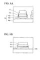
- the hard mask 18 when the hard mask 18 is constructed by the triple-layered structure consisting of the TiN film 18a, the P-SIN film 18c, and the SiO 2 film 18b and also the thickness of the SiO 2 film 18b is adjusted, only the P-SIN film 18c and the TiN film 18a may be left as the hard mask 18 in the state that the etching of the first conductive film 15 is ended.
- the hard mask 18 shown in FIG. 7 has the structure in which the TiN film 18a of 200 nm thickness, the P-SIN film 18c of 600 nm thickness, and the SiO 2 film 18b of 400 nm thickness, for example, are formed sequentially.
- the SiO 2 film 18b is formed by the CVD method using TEOS.
- FIG.8A is a perspective view showing the capacitor that is formed by etching the first conductive film 15, the ferroelectric film 16, and the second conductive film 17 while using the hard mask employing such a triple-layered structure, based on a microphotograph. Also, FIG.8B is a sectional view showing the same capacitor.
- an insulating film that is formed by introducing an impurity into the silicon oxide film may be employed as the material constituting the interlayer insulating layer in place of the silicon oxide film.
- a titanium compound film or a titanium film in addition to the TiN film may be employed as the lowermost layer of the above hard mask.
- the above film thicknesses shown in the conductive layers, the insulating films, and the dielectric layers are mere examples, and such film thicknesses are not limited to the above numerical values.
- an insulating material is employed as the uppermost layer of the hard mask that is used to pattern the first conductive film, the dielectric film, and the second conductive film formed on an insulating film, and then the removal of the uppermost layer is executed by interrupting the etching of the first conductive film. Therefore, when the uppermost insulating layer constituting the hard mask is removed by the etching, the underlying insulating film is never exposed, and thus the etching of the underlying insulating film of the capacitor can be suppressed.
- the uppermost layer of the hard mask is formed of silicon nitride, and then the capacitor is formed by etching the first conductive film, the dielectric film, and the second conductive film continuously while using this hard mask. Therefore, the uppermost insulating layer constituting the hard mask can be easily etched selectively to the insulating film after the capacitor is formed, and thus the etching of the underlying insulating film of the capacitor can be suppressed.
Landscapes
- Semiconductor Memories (AREA)
- Semiconductor Integrated Circuits (AREA)
Abstract
Description
Claims (19)
- A semiconductor device comprising:an insulating film (8) formed over a semiconductor substrate (1);a capacitor lower electrode (15a) formed on the insulating film (8) and having a discontinuous step on side surface;a capacitor dielectric film (16a) formed on the capacitor lower electrode (15a) and having a side surface that continues to an upper side surface of the capacitor lower electrode (15a); anda capacitor upper electrode (17a) formed on the capacitor dielectric film (16a) and having a side surface that continues to the side surface of the capacitor dielectric film (16a).
- A semiconductor device according to claim 1, further comprising:an impurity diffusion region (5a) formed in a surface region of the semiconductor substrate (1); anda conductive plug (9a) formed in the insulating film (8) and connected to the capacitor lower electrode (15a), and connected electrically to the impurity diffusion region (5a).
- A manufacturing method of a semiconductor device comprising the steps of:forming an insulating film (8) over a semiconductor substrate (1);forming sequentially a first conductive film (15), a dielectric film (16), and a second conductive film (17) over the insulating film (8);forming a first film (18a) made of one of metal and metal compound on the second conductive film (17);forming a second film (18b) made of insulating material on the first film (18a);forming a hard mask (18) by patterning the second film (18b) and the first film (18a) into a capacitor planar shape;forming a capacitor upper electrode (17a) by etching the second conductive film (17) in a region that is not covered with the hard mask (18);forming a capacitor dielectric film (16a) by etching the dielectric film (16) in the region that is not covered with the hard mask (8);etching the first conductive film (15) in the region that is not covered with the hard mask (18) up to a depth that does not expose the insulating film (8);removing the second film (18b) of the hard mask (18) by etching;forming a capacitor lower electrode (15a) by etching a remaining portion of the first conductive film (15) in the region, that is not covered with the hard mask (18), to the end; andremoving the first film (18a) of the hard mask (18) by the etching.
- A manufacturing method of a semiconductor device according to claim 3, wherein a step is formed on a side surface of the capacitor lower electrode (15a).
- A manufacturing method of a semiconductor device according to claim 3 or 4, wherein the second film (18b) is a silicon oxide film.
- A manufacturing method of a semiconductor device according to claim 5, wherein the silicon oxide film is formed while using TEOS as a source gas.
- A manufacturing method of a semiconductor device comprising the steps of:forming an insulating film (8) over a semiconductor substrate (1);forming sequentially a first conductive film (15) a dielectric film (16), and a second conductive film (17) over the insulating film (8);forming a first film (18a) made of one of metal and metal compound on the second conductive film (17);forming a second film (18c) made of a silicon nitride film, which is different material from the insulating film (8), on the first film (18a);forming a hard mask (18) by patterning the second film (18c) and the first film (18a) into a capacitor planar shape;forming a capacitor upper electrode (17a) by etching the second conductive film (17) in a region that is not covered with the hard mask (18);forming a capacitor dielectric film (16a) by etching the dielectric film (16) in the region that is not covered with the hard mask (18);forming a capacitor lower electrode (15a) by etching the first conductive film (15) in the region that is not covered with the hard mask (18);removing the second film (18c) of the hard mask (18) by etching using an etching gas containing fluorine and nitrogen; andremoving the first film (18a) of the hard mask (18) by the etching.
- A manufacturing method of a semiconductor device according to claim 7, wherein the silicon nitride film is formed by a plasma CVD method.
- A manufacturing method of a semiconductor device according to claim 7 or claim 8, wherein a temperature of a stage on which the semiconductor substrate is loaded is set to less than 60°C when the second film (18c) is removed.
- A manufacturing method of a semiconductor device according to any one of claims 7 to 9, wherein the etching gas is a mixed gas consisting of CF4 and N2, and a gas flow rate ratio of CF4 in the mixed gas is 20+10 flow rate %.
- A manufacturing method of a semiconductor device according to any one of claims 7 to 10, wherein a third film (18b) made of a silicon oxide film is formed on the first film (18a) before the first film (18a) and the second film (18c) are patterned, and the third film (18b) is patterned together with the first film (18a) and the second film (18c) to constitute a part of the hard mask (18).
- A manufacturing method of a semiconductor device according to claim 11, wherein a thickness of the third film (18b) is formed into such a thickness that is removed until an etching of the first conductive film (15) is ended.
- A manufacturing method of a semiconductor device according to any one of claims 3 to 12, wherein the insulating film (8) is formed of one of a silicon oxide film and a silicon oxide containing film.
- A manufacturing method of a semiconductor device according to any one of claims 3 to 13, wherein the first film (18a) is formed of one of a titanium film and a titanium compound film.
- A manufacturing method of a semiconductor device according to any one of claims 3 to 14, wherein the first conductive film (15) consists of at least one of a platinum- group metal film and a platinum-group metal oxide film.
- A manufacturing method of a semiconductor device according to any one of claims 3 to 15, wherein a mixed gas containing oxygen in a halogen gas is used as etching gases used to etch the first conductive film (15) and the second conductive film (17) respectively.
- A manufacturing method of a semiconductor device according to any one of claims 3 to 16, wherein the dielectric film (16) is a ferroelectric film, and a mixed gas consisting of a halogen gas and an inert gas is used as an etching gas of the dielectric film (16).
- A manufacturing method of a semiconductor device according to any one of claims 3 to 17, wherein an impurity diffusion region (5a) is formed in a surface region of the semiconductor substrate (1), and
further comprising the step of:forming a conductive plug (9a,11a which is connected electrically to the impurity diffusion region (5a) and connected to upper surface of the capacitor lower electrode (15a), in the insulating film (8). - A manufacturing method of a semiconductor device according to any one of claims 3 to 18, wherein removal of the hard mask (18) is carried out by down-flow etching.
Applications Claiming Priority (2)
| Application Number | Priority Date | Filing Date | Title |
|---|---|---|---|
| JP2002072199 | 2002-03-15 | ||
| JP2002072199A JP4014902B2 (en) | 2002-03-15 | 2002-03-15 | Manufacturing method of semiconductor device |
Publications (3)
| Publication Number | Publication Date |
|---|---|
| EP1345258A2 true EP1345258A2 (en) | 2003-09-17 |
| EP1345258A3 EP1345258A3 (en) | 2006-11-08 |
| EP1345258B1 EP1345258B1 (en) | 2011-08-03 |
Family
ID=27764565
Family Applications (1)
| Application Number | Title | Priority Date | Filing Date |
|---|---|---|---|
| EP03250684A Expired - Lifetime EP1345258B1 (en) | 2002-03-15 | 2003-02-03 | Semiconductor device and method of manufacturing the same |
Country Status (5)
| Country | Link |
|---|---|
| US (2) | US6746878B2 (en) |
| EP (1) | EP1345258B1 (en) |
| JP (1) | JP4014902B2 (en) |
| KR (1) | KR100848240B1 (en) |
| TW (1) | TWI222117B (en) |
Cited By (1)
| Publication number | Priority date | Publication date | Assignee | Title |
|---|---|---|---|---|
| WO2005031814A1 (en) * | 2003-09-26 | 2005-04-07 | Infineon Technologies Ag | A method for producing a ferroelectric capacitor and a ferroelectric capacitor device |
Families Citing this family (15)
| Publication number | Priority date | Publication date | Assignee | Title |
|---|---|---|---|---|
| JP2004023078A (en) * | 2002-06-20 | 2004-01-22 | Fujitsu Ltd | Method for manufacturing semiconductor device |
| JP2004039699A (en) * | 2002-06-28 | 2004-02-05 | Fujitsu Ltd | Semiconductor device and manufacturing method thereof |
| US6867053B2 (en) * | 2003-07-28 | 2005-03-15 | Infineon Technologies Ag | Fabrication of a FeRAM capacitor using a noble metal hardmask |
| US7105400B2 (en) * | 2003-09-30 | 2006-09-12 | Kabushiki Kaisha Toshiba | Manufacturing method of semiconductor device |
| US7061035B2 (en) * | 2003-10-01 | 2006-06-13 | Infineon Technologies Ag | Self-aligned V0-contact for cell size reduction |
| KR100584063B1 (en) * | 2003-12-31 | 2006-05-29 | 동부일렉트로닉스 주식회사 | Capacitor top metal etching method |
| JP4551725B2 (en) * | 2004-09-13 | 2010-09-29 | Okiセミコンダクタ株式会社 | Manufacturing method of semiconductor device |
| US7118959B2 (en) * | 2005-03-10 | 2006-10-10 | Texas Instruments Incorporated | Integrated circuit capacitor having antireflective dielectric |
| JPWO2006100737A1 (en) * | 2005-03-18 | 2008-08-28 | 富士通株式会社 | Manufacturing method of semiconductor device |
| KR100725451B1 (en) * | 2005-06-07 | 2007-06-07 | 삼성전자주식회사 | Manufacturing method of ferroelectric capacitor and manufacturing method of semiconductor device using same |
| JP4580284B2 (en) * | 2005-06-20 | 2010-11-10 | Okiセミコンダクタ株式会社 | Method for manufacturing ferroelectric element |
| US20070232014A1 (en) * | 2006-04-03 | 2007-10-04 | Honeywell International Inc. | Method of fabricating a planar MIM capacitor |
| JP4882548B2 (en) * | 2006-06-30 | 2012-02-22 | 富士通セミコンダクター株式会社 | Semiconductor device and manufacturing method thereof |
| US9536822B2 (en) * | 2008-10-13 | 2017-01-03 | Texas Instruments Incorporated | Drawn dummy FeCAP, via and metal structures |
| KR101088816B1 (en) * | 2009-06-04 | 2011-12-02 | 주식회사 하이닉스반도체 | Semiconductor device and manufacturing method thereof |
Family Cites Families (24)
| Publication number | Priority date | Publication date | Assignee | Title |
|---|---|---|---|---|
| KR100413649B1 (en) * | 1996-01-26 | 2004-04-28 | 마츠시타 덴끼 산교 가부시키가이샤 | Method of manufacturing semiconductor devices |
| JP3705513B2 (en) * | 1996-07-31 | 2005-10-12 | 株式会社小松製作所 | Triangular crawler device |
| JPH10223855A (en) * | 1997-02-06 | 1998-08-21 | Hitachi Ltd | Semiconductor memory device and method of manufacturing semiconductor memory device |
| JP3215345B2 (en) * | 1997-03-19 | 2001-10-02 | 富士通株式会社 | Method for manufacturing semiconductor device |
| US6396092B1 (en) * | 1997-03-27 | 2002-05-28 | Hitachi, Ltd. | Semiconductor device and method for manufacturing the same |
| JPH11186521A (en) * | 1997-12-22 | 1999-07-09 | Oki Electric Ind Co Ltd | Method for manufacturing semiconductor device |
| US6313539B1 (en) * | 1997-12-24 | 2001-11-06 | Sharp Kabushiki Kaisha | Semiconductor memory device and production method of the same |
| KR100319879B1 (en) * | 1998-05-28 | 2002-08-24 | 삼성전자 주식회사 | Method of forming lower electrode of capacitor using dry etching of platinum group metal film |
| US6277760B1 (en) * | 1998-06-26 | 2001-08-21 | Lg Electronics Inc. | Method for fabricating ferroelectric capacitor |
| JP3768357B2 (en) * | 1998-12-01 | 2006-04-19 | 富士通株式会社 | Manufacturing method of high dielectric capacitor |
| KR100329774B1 (en) * | 1998-12-22 | 2002-05-09 | 박종섭 | Method for forming capacitor of ferroelectric random access memory device |
| JP2002043540A (en) * | 1999-05-14 | 2002-02-08 | Toshiba Corp | Semiconductor device |
| US6611014B1 (en) * | 1999-05-14 | 2003-08-26 | Kabushiki Kaisha Toshiba | Semiconductor device having ferroelectric capacitor and hydrogen barrier film and manufacturing method thereof |
| US6420272B1 (en) * | 1999-12-14 | 2002-07-16 | Infineon Technologies A G | Method for removal of hard mask used to define noble metal electrode |
| US6534809B2 (en) * | 1999-12-22 | 2003-03-18 | Agilent Technologies, Inc. | Hardmask designs for dry etching FeRAM capacitor stacks |
| US6485988B2 (en) * | 1999-12-22 | 2002-11-26 | Texas Instruments Incorporated | Hydrogen-free contact etch for ferroelectric capacitor formation |
| US6603161B2 (en) * | 2000-03-10 | 2003-08-05 | Kabushiki Kaisha Toshiba | Semiconductor device having ferroelectric capacitor and method for manufacturing the same |
| JP4034492B2 (en) * | 2000-03-10 | 2008-01-16 | 株式会社東芝 | Manufacturing method of semiconductor memory device |
| JP2001274352A (en) * | 2000-03-27 | 2001-10-05 | Toshiba Corp | Semiconductor device and method of manufacturing the same |
| US6617208B2 (en) * | 2000-08-18 | 2003-09-09 | Texas Instruments Incorporated | High capacitance damascene capacitors |
| US6642564B2 (en) * | 2001-07-18 | 2003-11-04 | Matsushita Electric Industrial Co., Ltd. | Semiconductor memory and method for fabricating the same |
| KR100420122B1 (en) * | 2001-07-21 | 2004-03-02 | 삼성전자주식회사 | Ferroelectric memory device and method of fabricating the same |
| JP2003243621A (en) * | 2002-02-15 | 2003-08-29 | Fujitsu Ltd | Semiconductor device and manufacturing method thereof |
| JP2004095866A (en) * | 2002-08-30 | 2004-03-25 | Fujitsu Ltd | Semiconductor device and manufacturing method thereof |
-
2002
- 2002-03-15 JP JP2002072199A patent/JP4014902B2/en not_active Expired - Fee Related
-
2003
- 2003-01-29 TW TW092102037A patent/TWI222117B/en not_active IP Right Cessation
- 2003-01-29 US US10/352,930 patent/US6746878B2/en not_active Expired - Lifetime
- 2003-02-03 EP EP03250684A patent/EP1345258B1/en not_active Expired - Lifetime
- 2003-02-22 KR KR1020030011202A patent/KR100848240B1/en not_active Expired - Fee Related
-
2004
- 2004-04-26 US US10/831,178 patent/US7139161B2/en not_active Expired - Lifetime
Cited By (2)
| Publication number | Priority date | Publication date | Assignee | Title |
|---|---|---|---|---|
| WO2005031814A1 (en) * | 2003-09-26 | 2005-04-07 | Infineon Technologies Ag | A method for producing a ferroelectric capacitor and a ferroelectric capacitor device |
| US7001781B2 (en) | 2003-09-26 | 2006-02-21 | Infineon Technologies Ag | Method for producing a ferroelectric capacitor that includes etching with hardmasks |
Also Published As
| Publication number | Publication date |
|---|---|
| KR20030074150A (en) | 2003-09-19 |
| US20040196618A1 (en) | 2004-10-07 |
| TW200304670A (en) | 2003-10-01 |
| US7139161B2 (en) | 2006-11-21 |
| EP1345258A3 (en) | 2006-11-08 |
| EP1345258B1 (en) | 2011-08-03 |
| US20030173605A1 (en) | 2003-09-18 |
| US6746878B2 (en) | 2004-06-08 |
| KR100848240B1 (en) | 2008-07-24 |
| TWI222117B (en) | 2004-10-11 |
| JP4014902B2 (en) | 2007-11-28 |
| JP2003273326A (en) | 2003-09-26 |
Similar Documents
| Publication | Publication Date | Title |
|---|---|---|
| US7221015B2 (en) | Semiconductor device and method of manufacturing the same | |
| US6825076B2 (en) | Method of manufacturing the FeRAM semiconductor device with improved contact plug structure | |
| US7465657B2 (en) | Method of manufacturing a semiconductor device having a capacitor | |
| US8956881B2 (en) | Method of manufacturing a FeRAM device | |
| EP1345258B1 (en) | Semiconductor device and method of manufacturing the same | |
| KR100796915B1 (en) | Semiconductor device and manufacturing method thereof | |
| EP1341218B1 (en) | Semiconductor device manufacturing method | |
| JP3994017B2 (en) | Manufacturing method of semiconductor device | |
| EP1376673A2 (en) | Semiconductor device manufacturing method | |
| US20080179645A1 (en) | Semiconductor device and method of producing the same | |
| US7763545B2 (en) | Semiconductor device manufacturing method | |
| JP2004214544A (en) | Method for manufacturing semiconductor device | |
| JP4467891B2 (en) | Manufacturing method of semiconductor device | |
| JP4515492B2 (en) | Manufacturing method of semiconductor device |
Legal Events
| Date | Code | Title | Description |
|---|---|---|---|
| PUAI | Public reference made under article 153(3) epc to a published international application that has entered the european phase |
Free format text: ORIGINAL CODE: 0009012 |
|
| AK | Designated contracting states |
Kind code of ref document: A2 Designated state(s): AT BE BG CH CY CZ DE DK EE ES FI FR GB GR HU IE IT LI LU MC NL PT SE SI SK TR |
|
| AX | Request for extension of the european patent |
Extension state: AL LT LV MK RO |
|
| PUAL | Search report despatched |
Free format text: ORIGINAL CODE: 0009013 |
|
| AK | Designated contracting states |
Kind code of ref document: A3 Designated state(s): AT BE BG CH CY CZ DE DK EE ES FI FR GB GR HU IE IT LI LU MC NL PT SE SI SK TR |
|
| AX | Request for extension of the european patent |
Extension state: AL LT LV MK RO |
|
| 17P | Request for examination filed |
Effective date: 20070214 |
|
| 17Q | First examination report despatched |
Effective date: 20070323 |
|
| AKX | Designation fees paid |
Designated state(s): DE FR GB IT |
|
| RAP1 | Party data changed (applicant data changed or rights of an application transferred) |
Owner name: FUJITSU MICROELECTRONICS LIMITED |
|
| RAP1 | Party data changed (applicant data changed or rights of an application transferred) |
Owner name: FUJITSU SEMICONDUCTOR LIMITED |
|
| GRAP | Despatch of communication of intention to grant a patent |
Free format text: ORIGINAL CODE: EPIDOSNIGR1 |
|
| GRAS | Grant fee paid |
Free format text: ORIGINAL CODE: EPIDOSNIGR3 |
|
| GRAA | (expected) grant |
Free format text: ORIGINAL CODE: 0009210 |
|
| AK | Designated contracting states |
Kind code of ref document: B1 Designated state(s): DE FR GB IT |
|
| REG | Reference to a national code |
Ref country code: GB Ref legal event code: FG4D |
|
| REG | Reference to a national code |
Ref country code: DE Ref legal event code: R096 Ref document number: 60337889 Country of ref document: DE Effective date: 20110929 |
|
| PG25 | Lapsed in a contracting state [announced via postgrant information from national office to epo] |
Ref country code: IT Free format text: LAPSE BECAUSE OF FAILURE TO SUBMIT A TRANSLATION OF THE DESCRIPTION OR TO PAY THE FEE WITHIN THE PRESCRIBED TIME-LIMIT Effective date: 20110803 |
|
| PLBE | No opposition filed within time limit |
Free format text: ORIGINAL CODE: 0009261 |
|
| STAA | Information on the status of an ep patent application or granted ep patent |
Free format text: STATUS: NO OPPOSITION FILED WITHIN TIME LIMIT |
|
| 26N | No opposition filed |
Effective date: 20120504 |
|
| REG | Reference to a national code |
Ref country code: DE Ref legal event code: R097 Ref document number: 60337889 Country of ref document: DE Effective date: 20120504 |
|
| GBPC | Gb: european patent ceased through non-payment of renewal fee |
Effective date: 20120203 |
|
| REG | Reference to a national code |
Ref country code: FR Ref legal event code: ST Effective date: 20121031 |
|
| PG25 | Lapsed in a contracting state [announced via postgrant information from national office to epo] |
Ref country code: FR Free format text: LAPSE BECAUSE OF NON-PAYMENT OF DUE FEES Effective date: 20120229 Ref country code: GB Free format text: LAPSE BECAUSE OF NON-PAYMENT OF DUE FEES Effective date: 20120203 |
|
| PGFP | Annual fee paid to national office [announced via postgrant information from national office to epo] |
Ref country code: DE Payment date: 20190122 Year of fee payment: 17 |
|
| REG | Reference to a national code |
Ref country code: DE Ref legal event code: R119 Ref document number: 60337889 Country of ref document: DE |
|
| PG25 | Lapsed in a contracting state [announced via postgrant information from national office to epo] |
Ref country code: DE Free format text: LAPSE BECAUSE OF NON-PAYMENT OF DUE FEES Effective date: 20200901 |