EP1343170A2 - A magnetic storage device - Google Patents
A magnetic storage device Download PDFInfo
- Publication number
- EP1343170A2 EP1343170A2 EP03251202A EP03251202A EP1343170A2 EP 1343170 A2 EP1343170 A2 EP 1343170A2 EP 03251202 A EP03251202 A EP 03251202A EP 03251202 A EP03251202 A EP 03251202A EP 1343170 A2 EP1343170 A2 EP 1343170A2
- Authority
- EP
- European Patent Office
- Prior art keywords
- layer
- magnetic
- layers
- orientations
- reference layer
- Prior art date
- Legal status (The legal status is an assumption and is not a legal conclusion. Google has not performed a legal analysis and makes no representation as to the accuracy of the status listed.)
- Withdrawn
Links
Images






Classifications
-
- G—PHYSICS
- G11—INFORMATION STORAGE
- G11C—STATIC STORES
- G11C11/00—Digital stores characterised by the use of particular electric or magnetic storage elements; Storage elements therefor
- G11C11/02—Digital stores characterised by the use of particular electric or magnetic storage elements; Storage elements therefor using magnetic elements
- G11C11/14—Digital stores characterised by the use of particular electric or magnetic storage elements; Storage elements therefor using magnetic elements using thin-film elements
- G11C11/15—Digital stores characterised by the use of particular electric or magnetic storage elements; Storage elements therefor using magnetic elements using thin-film elements using multiple magnetic layers
-
- B—PERFORMING OPERATIONS; TRANSPORTING
- B82—NANOTECHNOLOGY
- B82Y—SPECIFIC USES OR APPLICATIONS OF NANOSTRUCTURES; MEASUREMENT OR ANALYSIS OF NANOSTRUCTURES; MANUFACTURE OR TREATMENT OF NANOSTRUCTURES
- B82Y25/00—Nanomagnetism, e.g. magnetoimpedance, anisotropic magnetoresistance, giant magnetoresistance or tunneling magnetoresistance
-
- G—PHYSICS
- G11—INFORMATION STORAGE
- G11C—STATIC STORES
- G11C11/00—Digital stores characterised by the use of particular electric or magnetic storage elements; Storage elements therefor
- G11C11/02—Digital stores characterised by the use of particular electric or magnetic storage elements; Storage elements therefor using magnetic elements
- G11C11/16—Digital stores characterised by the use of particular electric or magnetic storage elements; Storage elements therefor using magnetic elements using elements in which the storage effect is based on magnetic spin effect
- G11C11/161—Digital stores characterised by the use of particular electric or magnetic storage elements; Storage elements therefor using magnetic elements using elements in which the storage effect is based on magnetic spin effect details concerning the memory cell structure, e.g. the layers of the ferromagnetic memory cell
-
- G—PHYSICS
- G11—INFORMATION STORAGE
- G11C—STATIC STORES
- G11C11/00—Digital stores characterised by the use of particular electric or magnetic storage elements; Storage elements therefor
- G11C11/02—Digital stores characterised by the use of particular electric or magnetic storage elements; Storage elements therefor using magnetic elements
- G11C11/16—Digital stores characterised by the use of particular electric or magnetic storage elements; Storage elements therefor using magnetic elements using elements in which the storage effect is based on magnetic spin effect
- G11C11/165—Auxiliary circuits
- G11C11/1673—Reading or sensing circuits or methods
-
- H—ELECTRICITY
- H01—ELECTRIC ELEMENTS
- H01F—MAGNETS; INDUCTANCES; TRANSFORMERS; SELECTION OF MATERIALS FOR THEIR MAGNETIC PROPERTIES
- H01F10/00—Thin magnetic films, e.g. of one-domain structure
- H01F10/32—Spin-exchange-coupled multilayers, e.g. nanostructured superlattices
- H01F10/324—Exchange coupling of magnetic film pairs via a very thin non-magnetic spacer, e.g. by exchange with conduction electrons of the spacer
-
- H—ELECTRICITY
- H01—ELECTRIC ELEMENTS
- H01F—MAGNETS; INDUCTANCES; TRANSFORMERS; SELECTION OF MATERIALS FOR THEIR MAGNETIC PROPERTIES
- H01F10/00—Thin magnetic films, e.g. of one-domain structure
- H01F10/32—Spin-exchange-coupled multilayers, e.g. nanostructured superlattices
- H01F10/324—Exchange coupling of magnetic film pairs via a very thin non-magnetic spacer, e.g. by exchange with conduction electrons of the spacer
- H01F10/3254—Exchange coupling of magnetic film pairs via a very thin non-magnetic spacer, e.g. by exchange with conduction electrons of the spacer the spacer being semiconducting or insulating, e.g. for spin tunnel junction [STJ]
-
- H—ELECTRICITY
- H01—ELECTRIC ELEMENTS
- H01F—MAGNETS; INDUCTANCES; TRANSFORMERS; SELECTION OF MATERIALS FOR THEIR MAGNETIC PROPERTIES
- H01F10/00—Thin magnetic films, e.g. of one-domain structure
- H01F10/32—Spin-exchange-coupled multilayers, e.g. nanostructured superlattices
- H01F10/324—Exchange coupling of magnetic film pairs via a very thin non-magnetic spacer, e.g. by exchange with conduction electrons of the spacer
- H01F10/3268—Exchange coupling of magnetic film pairs via a very thin non-magnetic spacer, e.g. by exchange with conduction electrons of the spacer the exchange coupling being asymmetric, e.g. by use of additional pinning, by using antiferromagnetic or ferromagnetic coupling interface, i.e. so-called spin-valve [SV] structure, e.g. NiFe/Cu/NiFe/FeMn
- H01F10/3272—Exchange coupling of magnetic film pairs via a very thin non-magnetic spacer, e.g. by exchange with conduction electrons of the spacer the exchange coupling being asymmetric, e.g. by use of additional pinning, by using antiferromagnetic or ferromagnetic coupling interface, i.e. so-called spin-valve [SV] structure, e.g. NiFe/Cu/NiFe/FeMn by use of anti-parallel coupled [APC] ferromagnetic layers, e.g. artificial ferrimagnets [AFI], artificial [AAF] or synthetic [SAF] anti-ferromagnets
- H01F10/3277—Exchange coupling of magnetic film pairs via a very thin non-magnetic spacer, e.g. by exchange with conduction electrons of the spacer the exchange coupling being asymmetric, e.g. by use of additional pinning, by using antiferromagnetic or ferromagnetic coupling interface, i.e. so-called spin-valve [SV] structure, e.g. NiFe/Cu/NiFe/FeMn by use of anti-parallel coupled [APC] ferromagnetic layers, e.g. artificial ferrimagnets [AFI], artificial [AAF] or synthetic [SAF] anti-ferromagnets by use of artificial ferrimagnets [AFI] only
Definitions
- the present invention relates to the field of magnetic storage devices. More particularly, the present invention relates to a synthetic ferrimagnet reference layer for a magnetic storage device.
- MRAM Magnetic Random Access Memory
- DRAM Dynamic Random Access Memory
- SRAM Stable Random Access Memory
- Flash memory Flash memory
- MRAM can perform read and write operations much faster (by orders of magnitude) than conventional long-term storage devices such as hard drives.
- MRAM is more compact and consumes less power than hard drives.
- a typical MRAM device includes an array of memory cells, word lines extending along rows of the memory cells, and bit lines extending along columns of the memory cells. Each memory cell is located at a cross point of a word line and a bit line.
- the memory cells may be based on tunneling magneto-resistive (TMR) devices such as spin dependent tunneling junctions (SDT).
- TMR tunneling magneto-resistive
- SDT spin dependent tunneling junctions
- a typical SDT junction includes a pinned layer, a sense layer and an insulating tunnel barrier sandwiched between the pinned and sense layers.
- the pinned layer has a magnetization orientation that is fixed so as not to rotate in the presence of an applied magnetic field in a range of interest.
- the sense layer has a magnetization that can be oriented in either of two directions: the same direction as the pinned layer magnetization or the opposite direction of the pinned layer magnetization.
- the magnetization orientation of the pinned layer may be fixed by an underlying antiferromagnetic (AF) pinning layer.
- the AF pinning layer provides a large exchange field, which holds the magnetization of the pinned layer in one direction.
- Underlying the AF layer are usually first and second seed layers.
- the first seed layer allows the second seed layer to be grown with a crystal structure orientation.
- the second seed layer establishes a crystal structure orientation for the AF pinning layer.
- the pinned layer in some conventional magneto-resistive memory devices may have a net magnetic moment, which leads to undesirable effects.
- One such effect is that of a demagnetizing field.
- the magnetic layer of the pinned layer reaches and interacts with the sense layer.
- the sense layer stores information by the orientation of its magnetization, clearly its magnetic orientation must be preserved.
- the interaction of the magnetic field from the pinned layer may lead to loss of data if this magnetic field becomes too strong.
- a second problem is that the presence of the magnetic field from the pinned layer requires that an asymmetric magnetic field be used to switch the state of the data layer, which adds to the complexity of the writing process.
- a still further problem is that the tolerance for stray magnetic fields during writing is lowered.
- pinned structures Another disadvantage of pinned structures is that the materials needed to achieve pinning (e.g., the AF pinning layer and the seed layer) are both complicated and expensive to fabricate.
- embodiments of the present invention provide a synthetic ferrimagnet reference layer for a magnetic storage device.
- Embodiments of the present invention provide for a device that minimizes a demagnetizing field that may be present in conventional magnetic storage devices.
- a synthetic ferrimagnet reference layer for a magnetic storage device is disclosed.
- the reference layer has first and second layers of magnetic material operable to be magnetized in first and second magnetic orientations.
- a spacer layer between the layers of magnetic material is of suitable dimensions to magnetically couple the magnetic layers in opposite directions.
- the layers of magnetic material have substantially the same coercivities.
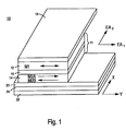
- a magnetic memory device 10 includes a magnetic tunnel junction 11 having a data layer 12, a reference layer 14, and a tunnel barrier 16 between the data and reference layers 12 and 14. Both layers 12 and 14 may be made of a ferromagnetic material.
- the data layer 12 has a magnetization (represented by the vector M1) that can be orientated in either of two directions, typically along the easy axis (EA1) of the data layer 12.
- the reference layer 14 may be constructed to have a net magnetic moment that is substantially zero. Hence, it may be stated that the net magnetization vector of the reference layer 14 is substantially zero. However, the reference layer 14 may have multiple magnetization vectors, such as, for example, magnetization vector M2A and M2B. These two vectors may be equal and opposite and hence may cancel each other at a distance. However, magnetization vector M2A may be closer to the tunnel barrier 16 than is magnetization vector M2B. The two magnetization vectors M2A and M2B may be orientated in either of two directions, typically along the y-axis. However, the magnetization vectors M2A and M2B are not necessarily orthogonal to the easy axis (EA2) of the reference layer 14.
- EA2A and M2B easy axis
- the orientation of the magnetic tunnel junction 11 may be referred to as being "parallel.” If the magnetization vectors (M1 and M2A) of the data and reference layers 12 and 14 are pointing in opposite directions, the orientation of the magnetic tunnel junction 11 may be referred to as being "anti-parallel.” These two orientations, parallel and anti-parallel, may correspond to logic values of '0' and '1'. The logic value that is represented by which orientation is arbitrary.
- the insulating tunnel barrier 16 allows quantum mechanical tunneling to occur between the data and reference layers 12 and 14. This tunneling phenomenon is electron spin dependent, causing the resistance of the magnetic tunnel junction 11 to be a function of the relative orientations of the magnetization vectors (M1 and M2A) of the data and reference layers 12 and 14. Thus, a bit may be stored by establishing the magnetization orientation of the data 12 and reference layers 14 to be different.
- the resistance of the magnetic tunnel junction 11 is a first value (R) if the magnetization orientation of the magnetic tunnel junction 11 is parallel and a second value (R+ ⁇ R) if the magnetization orientation is anti-parallel.
- the present invention is not limited to the magnetization orientation of the two layers relative to each other being either parallel or anti-parallel.
- the magnetic orientation of each layer may be selected such that the measured resistance between the layers is different for two different states.
- the two stable orientations may comprise a first range of angles and a second range of angles between the magnetic orientation magnetization vectors (M1 and M2A) of the data and reference layers 12 and 14, wherein the electrical resistance across the tunnel layer has first and second resistances corresponding to the two stables orientations.
- the insulating tunnel barrier 16 may be made of aluminum oxide (Al 2 O 3 ), silicon dioxide (SiO 2 ), tantalum oxide (Ta 2 O 5 ), silicon nitride (SiN 4 ), aluminum nitride (AIN x ), or magnesium oxide (MgO). Other dielectrics and certain semiconductor materials may be used for the insulating tunnel barrier 16. Thickness of the insulating tunnel barrier 16 may range from about 0.5 nanometers to about three nanometers. However, the present invention is not limited to this range.
- the data layer 12 may be made of a ferromagnetic material.
- the reference layer 14 may be implemented as a synthetic ferrimagnet (SF), also known as an artificial antiferromagnet.
- SF synthetic ferrimagnet
- a first conductor 18 extending along the y-axis is in contact with the data layer 12.
- a second conductor 20 extending along the x-axis is in contact with the reference layer 14.
- the first and second conductors 18 and 20 are shown as being orthogonal. However, the present invention is not limited to an orthogonal orientation.
- Below the second conductor 20 is a third conductor 22, which also extends along the x-axis.
- An electrical insulator 24 e.g., a layer of dielectric material
- the conductors 18, 20 and 22 may be made of an electrically conductive material such as aluminum, copper, gold or silver.
- the synthetic ferrimagnet reference layer 14 may include first and second ferromagnetic layers 50 and 52 separated by a spacer layer 54 (e.g., the spacer layer 54 may be metallic).
- the ferromagnetic layers 50 and 52 may be made of a material such as, for example, cobalt iron (CoFe), nickel iron (NiFe), Cobalt (Co), etc.
- the spacer layer 54 may be made of an electrically conductive, magnetically non-conductive material such as, for example, Ruthenium (Ru), Rhenium (Re), Rhodium (Rh), Copper (Cu), Tellurium (Te), Chromium (Cr), etc.
- the dimensions (e.g., thickness) of the spacer layer 54 may be selected to cause the first and second ferromagnetic layers 50 and 52 to be coupled, such that their magnetic orientations are anti-parallel, as seen in Figures 2A and 2B.
- the thickness may depend on the material that the spacer layer 54 is formed from. In one embodiment, the thickness may be between about 0.2 nm and 2 nm. However, other thicknesses may be suitable to couple the two ferromagnetic layers 50 and 52.
- the magnetization vector of the upper ferromagnetic layer 52 (M2A) is shown along the negative y-axis.
- the magnetization vector of the lower ferromagnetic layer 50 (M2B) is shown along the positive y-axis, in Figure 2A.
- the ultra-low coercivity allows the magnetization vectors (M2A and M2B) of the SF reference layer 14 to be switched easily between the orientations shown in Figures 2A and 2B.
- the orientations of the magnetic vectors M2A and M2B for the ferromagnetic layers 50 and 52 may be in any direction just before the magnetic field is applied. Once the magnetic field is applied, their orientations are known. Only a very small magnetic field needs to be applied to the ferromagnetic layers 50 and 52 to push the magnetization vectors M2A and M2B to known positions shown in Figure 2A or 2B, (e.g., orthogonal to the applied magnetic field).
- the synthetic ferrimagnet reference layer 14 comprises more than two ferromagnetic layers.
- adjacent ferromagnetic layers may be joined by spacer layers 54 and may have their magnetic orientations in opposite directions.
- the net magnetic moment of the synthetic ferrimagnet reference layer 14 is substantially zero.
- Embodiments provide for both even and odd numbers of ferromagnetic layers in a synthetic ferrimagnet reference layer 14.
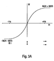
- Figure 3A illustrates a typical hysteresis loop for a synthetic ferrimagnet reference layer 14 with exemplary dimensions and materials of CoFe 3nm/Ru 0.75nm/CoFe 3nm.
- each ferromagnetic layer 50, 52 may, for example, have a coercivity of about 10-100 Oersted (e.g., about 800 - 8000 Amperes/Meter) and have similar hysteresis loops.
- the present invention is not limited to this range of coercivities.
- the coercivities of the two ferromagnetic layers 50 and 52 may be substantially the same. This may be accomplished by using the same thickness of identical materials; however, the present invention is not limited to this way of achieving substantially identical coercivities.
- each ferromagnetic layer has the same coercivity.
- the combined coercivities of the ferromagnetic layers may cause the net magnetic moment of the reference layer 14 to be substantially zero.
- the hysteresis loop for the combined ferromagnetic layers 50 and 52 may pass though the origin where the net magnetic moment is zero.
- the combined moments of the ferromagnetic layers causes the net magnetic moment of the reference layer 14 to be substantially zero.
- the ferromagnetic layers do not have identical moments.
- Exchange coupling between the magnetization vectors M2A, M2B of the two ferromagnetic layers 50 and 52 may be very strong. Consequently, a very large magnetic field may be needed to saturate the magnetization vectors M2A, M2B of the ferromagnetic layers 50 and 52. For example, a field of 4000 Oersted (e.g., 3.2 x 10 5 Amperes/Meter) may be needed to completely rotate both the ferromagnetic layers 50 and 52 in the same direction.
- the exchange coupling may be made suitably strong such that at normal operating conditions, very little rotation occurs and the ferromagnetic layers 50 and 52 point 180 degrees apart.
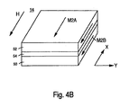
- the ferromagnetic layers 50 and 52 when exposed to a relatively high magnetic field, the ferromagnetic layers 50 and 52 may rotate and orient themselves in the direction of the applied field. This is illustrated by the parallel double arrows below the hysteresis loop at the point when Hs is large (positive or negative). This is also illustrated in Figures 4A and 4B, in which the magnetization vectors M2A and M2B are shown as being parallel to the applied magnetic field (H).
- the fields required to saturate both the ferromagnetic layers 50 and 52 are substantially larger than normally used to read a magneto-resistive device.
- Figure 3B illustrates a detail of the hysteresis loop of Figure 3A showing low applied magnetic fields.
- the amount of rotation away from 180 degrees between the magnetic vectors M2A and M2B may be very small.
- the angle theta may be approximately 2 degrees.
- Theta is the angle by which the magnetic vectors M2A and M2B deviate from being orthogonal to the applied field.
- the magnetic vectors are nearly orthogonal to the applied field under normal operating conditions. This state is also shown in Figures 2A and 2B.
- Step 510 of the process is storing bit of information in the data layer 12. This may be achieved by applying one or more currents to selected word lines 18 and/or bit lines 20 to set the magnetization vector M1 in the data layer 12.
- the magnetic orientations M2A, M2B of the ferromagnetic layers 50 and 52 are not critical at this time, as they may be established later.
- data may be written to the magnetic tunnel junction 11 by supplying write currents to the first and second conductors 18 and 20.
- the current supplied to the first conductor 18 creates a magnetic field about the first conductor 18, and the current supplied to the second conductor 20 creates a magnetic field about the second conductor 20.
- the two magnetic fields when combined, exceed the coercivity of the data layer 12 and, therefore, cause the magnetization vector (M1) of the data layer 12 to be set in a desired orientation (the orientation will depend upon the directions of the currents supplied to the first and second conductors 18 and 20).
- the magnetization will be set to either the orientation that corresponds to a logic '1' or the orientation that corresponds to a logic '0'.
- the magnetization vector (M1) of the data layer 12 retains its orientation.
- the magnetization vectors (M2A and M2B) of the ferromagnetic layers 50 and 52 may be affected by the write process and may or may not retain that orientation. If the reference layer 14 is "ultra-soft," the magnetization vectors (M2A and M2B) may lose their magnetization orientations when the write currents are removed from the first and second conductors 18 and 20.
- the third conductor 22 may be used to assist with write operations. By supplying a current to the third conductor 22 during write operations, the resulting magnetic field about the third conductor 22 may combine with the other two magnetic fields to help set the magnetization vector (M1) of the data layer 12 in the desired orientation.
- a magnetic field is applied to a reference layer 14 to establish a magnetic orientation (e.g., M2A) in a layer (e.g., ferromagnetic layer 52) of the reference layer 14 that is substantially orthogonal to the magnetic field.
- the reference layer 14 itself has first and second layers that have substantially the same coercivity and are magnetically coupled in opposite directions.
- the magnetic orientation of the first ferromagnetic layer 52 of the reference layer 14 is either substantially parallel or substantially anti-parallel to the magnetic orientation M1 in the data layer 12.
- a current may be supplied to the third conductor 22, and the resulting magnetic field causes the magnetization vectors M2A and M2B of the ferromagnetic layers 50 and 52 to assume a specific orientation. Because the third conductor 22 is farther from one ferromagnetic layer 50 or 52 than the other, the magnetic orientation may be known by its preference to favor one direction in each ferromagnetic layer 50, 52, the direction depending, in part, on the direction of the current through the third conductor 22. The resulting magnetic field does not affect the magnetization vector (M1) of the data layer 12. Furthermore, since the coercivity of the reference layer 14 is extremely low, the magnitude of the third conductor current may be low. For example, the coercivity of the balanced synthetic ferrimagnet reference layer 14 may be only a few Oersteds (e.g., a few hundred Amperes/Meter).
- step 530 the resistance between the first ferromagnetic layer 52 and the data layer 12 is measured to determine the magnetic orientation M1 of the data layer 12. In this fashion, the bit stored in the storage device is determined.
- This step may be accomplished by applying a voltage across the magnetic tunnel junction 11 as the current is supplied to the third conductor 22.
- the first and second conductors 18 and 20 may be used to apply the voltage across the magnetic tunnel junction 11.
- the voltage causes a sense current to flow through the magnetic tunnel junction 11.
- the sensed current (I s ) is inversely proportional to the resistance of the magnetic tunnel junction 11.
- FIG. 6 illustrates an MRAM device 610 including an array 612 of magnetic tunnel junctions 11.
- the magnetic tunnel junctions 11 are arranged in rows and columns, with the rows extending along a y-direction and the columns extending along an x-direction. Only a relatively small number of the magnetic tunnel junctions 11 are shown to simplify the illustration of the MRAM device 610. In practice, arrays of any size may be used.
- Electrically conductive elements functioning as word lines 18 extend along the x-direction in a plane on one side of the array 612.
- the word lines 18 are in contact with the data layers 12 of the magnetic tunnel junctions 11.
- Electrically conductive elements functioning as bit lines 20 extend along the y-direction in a plane on an adjacent side of the array 612.
- the bit lines 20 are in contact with the reference layers 14 of the magnetic tunnel junctions 11. There may be one word line 18 for each row of the array 612 and one bit line 20 for each column of the array 612.
- Each magnetic memory tunnel junction 11 is located at a cross point of a word line 18 and a bit line 20.
- the MRAM device 610 also includes first and second row decoders 614a and 614b, first and second column decoders 616a and 616b, and a read/write circuit 618.
- the read/write circuit 618 includes a sense amplifier 620, ground connections 622, a row current source 624, a voltage source 626, and a column current source 628.
- the first row decoder 614a connects one end of a selected word line 18 to the row current source 624
- the second row decoder 614b connects an opposite end of the selected word line 18 to ground
- the first column decoder 616a connects one end of a selected bit line 20 to ground
- the second column decoder 616b connects the opposite end of the selected bit line 20 to the column current source 628.
- write currents flow through the selected word and bit lines 18 and 20.
- the write currents create magnetic fields, which cause the magnetic tunnel junction 11 to switch.
- the column decoders 616a and 616b may also cause a write current to flow through the read line 22 crossing the selected magnetic tunnel junction 11. This third write current creates an additional magnetic field that assists in switching the selected magnetic tunnel junction 11.
- the easy axis of the data layers 12 may be oriented in the y-direction.
- the data layers 12 may have their magnetic vectors in the y-direction.
- the first and second column decoders 616a and 616b may cause a steady read (reference) current to flow through the read line 22 crossing the selected magnetic tunnel junction 11.
- the read current will generate a magnetic field that causes the magnetization vectors M2A and M2B to be oriented parallel to the word lines 18.
- the first row decoder 614a connects the voltage source 626 to a selected word line 18, and the first column decoder 616a connects a selected bit line 20 to a virtual ground input of the sense amplifier 620.
- a sense current flows through the selected magnetic tunnel junction 11 to the input of the sense amplifier 620.
- the resistance of the selected magnetic tunnel junction 11 may be determined.
- the present invention is not limited to this method of determining the resistance of the magnetic tunnel junctions 11.
- the magnetic tunnel junctions 11 described thus far include individual reference layers 14, with each reference layer 14 having the same geometry as its corresponding data layer 12 and tunnel barrier 16.
- the present invention is not limited to reference layers 14 having the same geometry as the data layers and tunnel barriers. Instead, the reference layers 14 may have the same geometry as the word and bit lines 18 and 20, or otherwise.
Landscapes
- Engineering & Computer Science (AREA)
- Chemical & Material Sciences (AREA)
- Crystallography & Structural Chemistry (AREA)
- Power Engineering (AREA)
- Nanotechnology (AREA)
- Computer Hardware Design (AREA)
- Mram Or Spin Memory Techniques (AREA)
- Hall/Mr Elements (AREA)
- Semiconductor Memories (AREA)
- Magnetic Record Carriers (AREA)
Abstract
Description
- The present invention relates to the field of magnetic storage devices. More particularly, the present invention relates to a synthetic ferrimagnet reference layer for a magnetic storage device.
- Magnetic Random Access Memory (MRAM) is a non-volatile memory that has lower power consumption than short-term memory such as DRAM, SRAM and Flash memory. MRAM can perform read and write operations much faster (by orders of magnitude) than conventional long-term storage devices such as hard drives. In addition, MRAM is more compact and consumes less power than hard drives.
- A typical MRAM device includes an array of memory cells, word lines extending along rows of the memory cells, and bit lines extending along columns of the memory cells. Each memory cell is located at a cross point of a word line and a bit line.
- The memory cells may be based on tunneling magneto-resistive (TMR) devices such as spin dependent tunneling junctions (SDT). A typical SDT junction includes a pinned layer, a sense layer and an insulating tunnel barrier sandwiched between the pinned and sense layers. The pinned layer has a magnetization orientation that is fixed so as not to rotate in the presence of an applied magnetic field in a range of interest. The sense layer has a magnetization that can be oriented in either of two directions: the same direction as the pinned layer magnetization or the opposite direction of the pinned layer magnetization. If the magnetizations of the pinned and sense layers are in the same direction, the orientation of the SDT junction is said to be "parallel." If the magnetizations of the pinned and sense layers are in opposite directions, the orientation of the SDT junction is said to be "anti-parallel." These two stable orientations, parallel and anti-parallel, may correspond to logic values of '0' and '1'.
- The magnetization orientation of the pinned layer may be fixed by an underlying antiferromagnetic (AF) pinning layer. The AF pinning layer provides a large exchange field, which holds the magnetization of the pinned layer in one direction. Underlying the AF layer are usually first and second seed layers. The first seed layer allows the second seed layer to be grown with a crystal structure orientation. The second seed layer establishes a crystal structure orientation for the AF pinning layer.
- The pinned layer in some conventional magneto-resistive memory devices may have a net magnetic moment, which leads to undesirable effects. One such effect is that of a demagnetizing field. For example, the magnetic layer of the pinned layer reaches and interacts with the sense layer. As the sense layer stores information by the orientation of its magnetization, clearly its magnetic orientation must be preserved. Thus, the interaction of the magnetic field from the pinned layer may lead to loss of data if this magnetic field becomes too strong. A second problem is that the presence of the magnetic field from the pinned layer requires that an asymmetric magnetic field be used to switch the state of the data layer, which adds to the complexity of the writing process. A still further problem is that the tolerance for stray magnetic fields during writing is lowered.
- As it is desirable to fabricate high capacity memories, it is desirable to fabricate an array of such memory cells as dense as possible. Unfortunately, the cumulative demagnetizing effects of all of the reference layers may constrain how densely the memory cells may be packed.
- Another disadvantage of pinned structures is that the materials needed to achieve pinning (e.g., the AF pinning layer and the seed layer) are both complicated and expensive to fabricate.
- Therefore, a need exists for an information storage device using magneto-resistive memory cells. A further need exists for such a device that minimizes a demagnetizing field that may be present in conventional magnetic storage devices. A still further need exists for a device that may be fabricated more economically and with fewer and simpler materials than conventional magnetic storage devices.
- Accordingly, embodiments of the present invention provide a synthetic ferrimagnet reference layer for a magnetic storage device. Embodiments of the present invention provide for a device that minimizes a demagnetizing field that may be present in conventional magnetic storage devices. A synthetic ferrimagnet reference layer for a magnetic storage device is disclosed. The reference layer has first and second layers of magnetic material operable to be magnetized in first and second magnetic orientations. A spacer layer between the layers of magnetic material is of suitable dimensions to magnetically couple the magnetic layers in opposite directions. The layers of magnetic material have substantially the same coercivities.
- The accompanying drawings, which are incorporated in and form a part of this specification, illustrate embodiments of the invention and, together with the description, serve to explain the principles of the invention:
- FIGURE 1 is an illustration of a magnetic memory device according to embodiments of the present invention.
- FIGURE 2A and FIGURE 2B are illustrations of reference layers according to embodiments of the present invention.
- FIGURE 3A is an illustration of a hysteresis loop for a reference layer according to embodiments of the present invention.
- FIGURE 3B is a magnified illustration of the hysteresis loop of FIGURE 3A for a reference layer according to embodiments of the present invention.
- FIGURE 4A and FIGURE 4B are illustrations of reference layers according to embodiments of the present invention.
- FIGURE 5 is a flowchart of steps of a process of reading a bit on a magnetic memory device according to embodiments of the present invention.
- FIGURE 6 is an illustration of a magnetic storage device according to embodiments of the present invention.
- In the following detailed description of the present invention, numerous specific details are set forth in order to provide a thorough understanding of the present invention. However, it will be obvious to one skilled in the art that the present invention may be practiced without these specific details or by using alternate elements or methods. In other instances well known methods, procedures, components, and circuits have not been described in detail as not to unnecessarily obscure aspects of the present invention.
- Referring to Figure 1, a
magnetic memory device 10 includes amagnetic tunnel junction 11 having adata layer 12, areference layer 14, and atunnel barrier 16 between the data andreference layers layers data layer 12 has a magnetization (represented by the vector M1) that can be orientated in either of two directions, typically along the easy axis (EA1) of thedata layer 12. - The
reference layer 14 may be constructed to have a net magnetic moment that is substantially zero. Hence, it may be stated that the net magnetization vector of thereference layer 14 is substantially zero. However, thereference layer 14 may have multiple magnetization vectors, such as, for example, magnetization vector M2A and M2B. These two vectors may be equal and opposite and hence may cancel each other at a distance. However, magnetization vector M2A may be closer to thetunnel barrier 16 than is magnetization vector M2B. The two magnetization vectors M2A and M2B may be orientated in either of two directions, typically along the y-axis. However, the magnetization vectors M2A and M2B are not necessarily orthogonal to the easy axis (EA2) of thereference layer 14. - If the magnetizations vectors of the data and
reference layers 12 and 14 (M1 and M2A) are pointing in the same direction, the orientation of themagnetic tunnel junction 11 may be referred to as being "parallel." If the magnetization vectors (M1 and M2A) of the data andreference layers magnetic tunnel junction 11 may be referred to as being "anti-parallel." These two orientations, parallel and anti-parallel, may correspond to logic values of '0' and '1'. The logic value that is represented by which orientation is arbitrary. - The
insulating tunnel barrier 16 allows quantum mechanical tunneling to occur between the data andreference layers magnetic tunnel junction 11 to be a function of the relative orientations of the magnetization vectors (M1 and M2A) of the data andreference layers data 12 andreference layers 14 to be different. For example, the resistance of themagnetic tunnel junction 11 is a first value (R) if the magnetization orientation of themagnetic tunnel junction 11 is parallel and a second value (R+ ΔR) if the magnetization orientation is anti-parallel. However, the present invention is not limited to the magnetization orientation of the two layers relative to each other being either parallel or anti-parallel. More generally, the magnetic orientation of each layer may be selected such that the measured resistance between the layers is different for two different states. The two stable orientations may comprise a first range of angles and a second range of angles between the magnetic orientation magnetization vectors (M1 and M2A) of the data andreference layers - The insulating
tunnel barrier 16 may be made of aluminum oxide (Al2O3), silicon dioxide (SiO2), tantalum oxide (Ta2O5), silicon nitride (SiN4), aluminum nitride (AINx), or magnesium oxide (MgO). Other dielectrics and certain semiconductor materials may be used for the insulatingtunnel barrier 16. Thickness of the insulatingtunnel barrier 16 may range from about 0.5 nanometers to about three nanometers. However, the present invention is not limited to this range. - The
data layer 12 may be made of a ferromagnetic material. Thereference layer 14 may be implemented as a synthetic ferrimagnet (SF), also known as an artificial antiferromagnet. - A
first conductor 18 extending along the y-axis is in contact with thedata layer 12. Asecond conductor 20 extending along the x-axis is in contact with thereference layer 14. The first andsecond conductors second conductor 20 is athird conductor 22, which also extends along the x-axis. An electrical insulator 24 (e.g., a layer of dielectric material) separates the second andthird conductors conductors - Referring now to Figures 2A and 2B, the synthetic
ferrimagnet reference layer 14 may include first and secondferromagnetic layers spacer layer 54 may be metallic). Theferromagnetic layers spacer layer 54 may be made of an electrically conductive, magnetically non-conductive material such as, for example, Ruthenium (Ru), Rhenium (Re), Rhodium (Rh), Copper (Cu), Tellurium (Te), Chromium (Cr), etc. - The dimensions (e.g., thickness) of the
spacer layer 54 may be selected to cause the first and secondferromagnetic layers spacer layer 54 is formed from. In one embodiment, the thickness may be between about 0.2 nm and 2 nm. However, other thicknesses may be suitable to couple the twoferromagnetic layers - For example, the magnetization vector of the upper ferromagnetic layer 52 (M2A) is shown along the negative y-axis. The magnetization vector of the lower ferromagnetic layer 50 (M2B) is shown along the positive y-axis, in Figure 2A.
- The ultra-low coercivity allows the magnetization vectors (M2A and M2B) of the
SF reference layer 14 to be switched easily between the orientations shown in Figures 2A and 2B. In practice, the orientations of the magnetic vectors M2A and M2B for theferromagnetic layers ferromagnetic layers - In some embodiments of the present invention, the synthetic
ferrimagnet reference layer 14 comprises more than two ferromagnetic layers. In these embodiments, adjacent ferromagnetic layers may be joined byspacer layers 54 and may have their magnetic orientations in opposite directions. The net magnetic moment of the syntheticferrimagnet reference layer 14 is substantially zero. Embodiments provide for both even and odd numbers of ferromagnetic layers in a syntheticferrimagnet reference layer 14. - Figure 3A illustrates a typical hysteresis loop for a synthetic
ferrimagnet reference layer 14 with exemplary dimensions and materials of CoFe 3nm/Ru 0.75nm/CoFe 3nm. Individually eachferromagnetic layer ferromagnetic layers reference layer 14 to be substantially zero. - As illustrated, the hysteresis loop for the combined
ferromagnetic layers reference layer 14 to be substantially zero. Thus, in some embodiments, the ferromagnetic layers do not have identical moments. - Exchange coupling between the magnetization vectors M2A, M2B of the two
ferromagnetic layers ferromagnetic layers ferromagnetic layers spacer layer 54, the exchange coupling may be made suitably strong such that at normal operating conditions, very little rotation occurs and theferromagnetic layers - Still referring to Figure 3A, when exposed to a relatively high magnetic field, the
ferromagnetic layers ferromagnetic layers - Under lower magnetic fields, there may be two stable magnetization orientations and these may be orthogonal to the applied field. Referring again to Figure 3, when near the y-axis, the arrows are shown as pointing up and down to indicate the magnetization vectors of the
ferromagnetic layers - Figure 3B illustrates a detail of the hysteresis loop of Figure 3A showing low applied magnetic fields. Under magnetic fields that are typical for read and write operations in a magneto-resistive device the amount of rotation away from 180 degrees between the magnetic vectors M2A and M2B may be very small. For example, when the applied magnetic field is approximately 100 Oersted (8000 Amperes/Meter), the angle theta may be approximately 2 degrees. Theta is the angle by which the magnetic vectors M2A and M2B deviate from being orthogonal to the applied field. Thus, the magnetic vectors are nearly orthogonal to the applied field under normal operating conditions. This state is also shown in Figures 2A and 2B.
- Referring now to the flowchart of Figure 5, an embodiment provides for a method of operating a magnetic storage device. Step 510 of the process is storing bit of information in the
data layer 12. This may be achieved by applying one or more currents to selectedword lines 18 and/orbit lines 20 to set the magnetization vector M1 in thedata layer 12. The magnetic orientations M2A, M2B of theferromagnetic layers - For example, in one embodiment, data may be written to the
magnetic tunnel junction 11 by supplying write currents to the first andsecond conductors first conductor 18 creates a magnetic field about thefirst conductor 18, and the current supplied to thesecond conductor 20 creates a magnetic field about thesecond conductor 20. The two magnetic fields, when combined, exceed the coercivity of thedata layer 12 and, therefore, cause the magnetization vector (M1) of thedata layer 12 to be set in a desired orientation (the orientation will depend upon the directions of the currents supplied to the first andsecond conductors 18 and 20). The magnetization will be set to either the orientation that corresponds to a logic '1' or the orientation that corresponds to a logic '0'. - After write currents are removed from the
conductors data layer 12 retains its orientation. The magnetization vectors (M2A and M2B) of theferromagnetic layers reference layer 14 is "ultra-soft," the magnetization vectors (M2A and M2B) may lose their magnetization orientations when the write currents are removed from the first andsecond conductors - In one embodiment, the
third conductor 22 may be used to assist with write operations. By supplying a current to thethird conductor 22 during write operations, the resulting magnetic field about thethird conductor 22 may combine with the other two magnetic fields to help set the magnetization vector (M1) of thedata layer 12 in the desired orientation. - In
step 520, a magnetic field is applied to areference layer 14 to establish a magnetic orientation (e.g., M2A) in a layer (e.g., ferromagnetic layer 52) of thereference layer 14 that is substantially orthogonal to the magnetic field. Thereference layer 14 itself has first and second layers that have substantially the same coercivity and are magnetically coupled in opposite directions. The magnetic orientation of the firstferromagnetic layer 52 of thereference layer 14 is either substantially parallel or substantially anti-parallel to the magnetic orientation M1 in thedata layer 12. - For example, a current may be supplied to the
third conductor 22, and the resulting magnetic field causes the magnetization vectors M2A and M2B of theferromagnetic layers third conductor 22 is farther from oneferromagnetic layer ferromagnetic layer third conductor 22. The resulting magnetic field does not affect the magnetization vector (M1) of thedata layer 12. Furthermore, since the coercivity of thereference layer 14 is extremely low, the magnitude of the third conductor current may be low. For example, the coercivity of the balanced syntheticferrimagnet reference layer 14 may be only a few Oersteds (e.g., a few hundred Amperes/Meter). - In
step 530, the resistance between the firstferromagnetic layer 52 and thedata layer 12 is measured to determine the magnetic orientation M1 of thedata layer 12. In this fashion, the bit stored in the storage device is determined. This step may be accomplished by applying a voltage across themagnetic tunnel junction 11 as the current is supplied to thethird conductor 22. The first andsecond conductors magnetic tunnel junction 11. The voltage causes a sense current to flow through themagnetic tunnel junction 11. The sensed current (Is) is inversely proportional to the resistance of themagnetic tunnel junction 11. Thus, Is = V/R or Is = V/(R+ ΔR), where V is the applied Voltage, Is is the sensed current, R is the nominal resistance of thedevice 10, and ΔR is the difference in resistance between the parallel magnetization orientation and the anti-parallel magnetization orientation. - Reference is now made to Figure 6, which illustrates an
MRAM device 610 including anarray 612 ofmagnetic tunnel junctions 11. Themagnetic tunnel junctions 11 are arranged in rows and columns, with the rows extending along a y-direction and the columns extending along an x-direction. Only a relatively small number of themagnetic tunnel junctions 11 are shown to simplify the illustration of theMRAM device 610. In practice, arrays of any size may be used. - Electrically conductive elements functioning as word lines 18 extend along the x-direction in a plane on one side of the
array 612. The word lines 18 are in contact with the data layers 12 of themagnetic tunnel junctions 11. Electrically conductive elements functioning asbit lines 20 extend along the y-direction in a plane on an adjacent side of thearray 612. The bit lines 20 are in contact with the reference layers 14 of themagnetic tunnel junctions 11. There may be oneword line 18 for each row of thearray 612 and onebit line 20 for each column of thearray 612. Each magneticmemory tunnel junction 11 is located at a cross point of aword line 18 and abit line 20. - Electrically conductive elements functioning as read
lines 22 also extend along the y-direction. The read lines 22 may be further from the tunnel junctions than the bit lines 20, and may be insulated from the bit lines 20. TheMRAM device 610 also includes first andsecond row decoders second column decoders 616a and 616b, and a read/write circuit 618. The read/write circuit 618 includes asense amplifier 620,ground connections 622, a row current source 624, avoltage source 626, and a columncurrent source 628. - During a write operation on a selected
magnetic tunnel junction 11, thefirst row decoder 614a connects one end of a selectedword line 18 to the row current source 624, thesecond row decoder 614b connects an opposite end of the selectedword line 18 to ground, thefirst column decoder 616a connects one end of a selectedbit line 20 to ground, and the second column decoder 616b connects the opposite end of the selectedbit line 20 to the columncurrent source 628. As a result, write currents flow through the selected word andbit lines magnetic tunnel junction 11 to switch. Thecolumn decoders 616a and 616b may also cause a write current to flow through the readline 22 crossing the selectedmagnetic tunnel junction 11. This third write current creates an additional magnetic field that assists in switching the selectedmagnetic tunnel junction 11. - The easy axis of the data layers 12 may be oriented in the y-direction. Thus, the data layers 12 may have their magnetic vectors in the y-direction.
- During a read operation on a selected
magnetic tunnel junction 11, the first andsecond column decoders 616a and 616b may cause a steady read (reference) current to flow through the readline 22 crossing the selectedmagnetic tunnel junction 11. The read current will generate a magnetic field that causes the magnetization vectors M2A and M2B to be oriented parallel to the word lines 18. - While the read current is still applied, the
first row decoder 614a connects thevoltage source 626 to a selectedword line 18, and thefirst column decoder 616a connects a selectedbit line 20 to a virtual ground input of thesense amplifier 620. As a result, a sense current flows through the selectedmagnetic tunnel junction 11 to the input of thesense amplifier 620. In this fashion, the resistance of the selectedmagnetic tunnel junction 11 may be determined. However, the present invention is not limited to this method of determining the resistance of themagnetic tunnel junctions 11. - The
magnetic tunnel junctions 11 described thus far include individual reference layers 14, with eachreference layer 14 having the same geometry as its correspondingdata layer 12 andtunnel barrier 16. However, the present invention is not limited toreference layers 14 having the same geometry as the data layers and tunnel barriers. Instead, the reference layers 14 may have the same geometry as the word andbit lines - While the present invention has been described in particular embodiments, it should be appreciated that the present invention should not be construed as limited by such embodiments, but rather construed according to the below claims.
Claims (10)
- A reference layer for a magnetic storage device, said reference layer comprising:a first layer of magnetic material (50) operable to be magnetized in first and second magnetic orientations;a second layer of magnetic material (52) operable to be magnetized in first and second magnetic orientations;said first (50) and second layers (52) having substantially the same coercivities; anda spacer layer (16) between said first (50) and second layers (52), said spacer layer (16) of suitable dimensions to magnetically couple said first (50) and second layers (52) in opposite directions.
- The reference layer of Claim 1, wherein said first (50) and second layers (52) are constructed such that their magnetic orientations will tend to be substantially orthogonal to the direction of an applied magnetic field.
- The reference layer of Claim 1, wherein said first (50) and second layers (52) are ferromagnetic layers.
- The reference layer of Claim 1, wherein said spacer layer (16) is electrically conductive and magnetically non-conductive.
- The reference layer of Claim 1, wherein said first (50) and second layers (52) are substantially the same thickness.
- A magnetic storage device comprising:a synthetic ferrimagnet reference layer (14);a data layer (12) having a first and a second magnetic orientations;.a tunnel layer (16) between said reference layer 14 and said data layer (12); said reference layer (14) comprising:a first layer of magnetic material (50);a second layer of magnetic material (52);said first (50) and said second layers (52) operable to be magnetized to cause the net magnetic moment of the reference layer (14) to be substantially zero; anda spacer layer (16) between said first layer (50) and said second layer (52), said spacer layer (16) with dimensions to magnetically couple said first layer (50) and said second layer (52) in opposite directions;said reference layer (14) having two stable magnetic orientations, a first in which said first layer (50) is in a first direction and said second layer (52) is in an opposite direction and a second stable state in which said first layer (50) is in said opposite direction and said second layer (52) is in said first direction, said directions being substantially orthogonal to an applied magnetic field.
- The device of Claim 8, further comprising means for creating a magnetic orientation in said second layer (52) that is either substantially parallel or anti-parallel to said magnetic orientation of said data layer (12).
- The device of Claim 8, wherein said second layer (52) is positioned relative to said data layer (12) such that said two stable magnetic orientations comprise a first range of angles and a second range of angles relative to said magnetic orientation in said data layer (12), wherein the electrical resistance across said spacer layer (16) has first and second resistances corresponding to said two stable orientations.
- A synthetic ferrimagnet reference layer for a magnetic storage device, said reference layer comprising:a plurality of layers of magnetic material (50, 52) having first and second magnetic orientations;at least one spacer layer (16), said at least one spacer layer (12) between adjacent layers of said plurality of layers (50, 52), said at least one spacer layer (16) of suitable dimensions to magnetically couple said adjacent layers in opposite directions; andsaid plurality of layers of magnetic material (50, 52) operable to be magnetized to cause the net magnetic moment of the reference layer (14) to be substantially zero.
- The reference layer of Claim 9, wherein said plurality of layers of magnetic material (50, 52) are constructed such that their magnetic orientations will tend to be substantially orthogonal to the direction of an applied magnetic field.
Applications Claiming Priority (2)
| Application Number | Priority Date | Filing Date | Title |
|---|---|---|---|
| US93344 | 2002-03-06 | ||
| US10/093,344 US6625059B1 (en) | 2002-03-06 | 2002-03-06 | Synthetic ferrimagnet reference layer for a magnetic storage device |
Publications (2)
| Publication Number | Publication Date |
|---|---|
| EP1343170A2 true EP1343170A2 (en) | 2003-09-10 |
| EP1343170A3 EP1343170A3 (en) | 2003-11-19 |
Family
ID=27754047
Family Applications (1)
| Application Number | Title | Priority Date | Filing Date |
|---|---|---|---|
| EP03251202A Withdrawn EP1343170A3 (en) | 2002-03-06 | 2003-02-27 | A magnetic storage device |
Country Status (6)
| Country | Link |
|---|---|
| US (1) | US6625059B1 (en) |
| EP (1) | EP1343170A3 (en) |
| JP (1) | JP4477829B2 (en) |
| KR (1) | KR100978641B1 (en) |
| CN (1) | CN100419902C (en) |
| TW (1) | TW200304143A (en) |
Cited By (1)
| Publication number | Priority date | Publication date | Assignee | Title |
|---|---|---|---|---|
| EP2109123A1 (en) * | 2008-04-11 | 2009-10-14 | Northern Lights Semiconductor Corp. | Apparatus for storing electrical energy |
Families Citing this family (10)
| Publication number | Priority date | Publication date | Assignee | Title |
|---|---|---|---|---|
| US6967350B2 (en) * | 2002-04-02 | 2005-11-22 | Hewlett-Packard Development Company, L.P. | Memory structures |
| US7167391B2 (en) * | 2004-02-11 | 2007-01-23 | Hewlett-Packard Development Company, L.P. | Multilayer pinned reference layer for a magnetic storage device |
| US7102920B2 (en) * | 2004-03-23 | 2006-09-05 | Hewlett-Packard Development Company, L.P. | Soft-reference three conductor magnetic memory storage device |
| US7622784B2 (en) * | 2005-01-10 | 2009-11-24 | International Business Machines Corporation | MRAM device with improved stack structure and offset field for low-power toggle mode writing |
| KR101598833B1 (en) * | 2009-12-21 | 2016-03-03 | 삼성전자주식회사 | Magnetic memory device and method of operating the same |
| US8890266B2 (en) | 2011-01-31 | 2014-11-18 | Everspin Technologies, Inc. | Fabrication process and layout for magnetic sensor arrays |
| US9583696B2 (en) | 2014-03-12 | 2017-02-28 | Qualcomm Incorporated | Reference layer for perpendicular magnetic anisotropy magnetic tunnel junction |
| US9666215B2 (en) | 2015-10-28 | 2017-05-30 | International Business Machines Corporation | Termination layer-compensated tunneling magnetoresistance in ferrimagnetic Heusler compounds with high perpendicular magnetic anisotropy |
| JP2020042882A (en) * | 2018-09-12 | 2020-03-19 | キオクシア株式会社 | Magnetic memory |
| CN112700583B (en) * | 2020-12-16 | 2025-05-23 | 宁波希磁电子科技有限公司 | Magnetic identification device, method and system and measured object with magnetic codes |
Family Cites Families (7)
| Publication number | Priority date | Publication date | Assignee | Title |
|---|---|---|---|---|
| US5650958A (en) * | 1996-03-18 | 1997-07-22 | International Business Machines Corporation | Magnetic tunnel junctions with controlled magnetic response |
| US6072718A (en) * | 1998-02-10 | 2000-06-06 | International Business Machines Corporation | Magnetic memory devices having multiple magnetic tunnel junctions therein |
| US6501678B1 (en) * | 1999-06-18 | 2002-12-31 | Koninklijke Philips Electronics N.V. | Magnetic systems with irreversible characteristics and a method of manufacturing and repairing and operating such systems |
| JP2001067620A (en) * | 1999-08-24 | 2001-03-16 | Matsushita Electric Ind Co Ltd | Method of manufacturing magnetoresistive element |
| US6166948A (en) * | 1999-09-03 | 2000-12-26 | International Business Machines Corporation | Magnetic memory array with magnetic tunnel junction memory cells having flux-closed free layers |
| JP2001196658A (en) * | 2000-01-07 | 2001-07-19 | Fujitsu Ltd | Magnetic element and magnetic storage device |
| US6385082B1 (en) * | 2000-11-08 | 2002-05-07 | International Business Machines Corp. | Thermally-assisted magnetic random access memory (MRAM) |
-
2002
- 2002-03-06 US US10/093,344 patent/US6625059B1/en not_active Expired - Lifetime
- 2002-11-25 TW TW091134208A patent/TW200304143A/en unknown
-
2003
- 2003-02-27 EP EP03251202A patent/EP1343170A3/en not_active Withdrawn
- 2003-03-05 JP JP2003058137A patent/JP4477829B2/en not_active Expired - Lifetime
- 2003-03-05 KR KR1020030013710A patent/KR100978641B1/en not_active Expired - Fee Related
- 2003-03-06 CN CNB031199364A patent/CN100419902C/en not_active Expired - Lifetime
Cited By (1)
| Publication number | Priority date | Publication date | Assignee | Title |
|---|---|---|---|---|
| EP2109123A1 (en) * | 2008-04-11 | 2009-10-14 | Northern Lights Semiconductor Corp. | Apparatus for storing electrical energy |
Also Published As
| Publication number | Publication date |
|---|---|
| CN100419902C (en) | 2008-09-17 |
| EP1343170A3 (en) | 2003-11-19 |
| JP2003272374A (en) | 2003-09-26 |
| CN1442861A (en) | 2003-09-17 |
| TW200304143A (en) | 2003-09-16 |
| US20030169620A1 (en) | 2003-09-11 |
| KR100978641B1 (en) | 2010-08-27 |
| JP4477829B2 (en) | 2010-06-09 |
| US6625059B1 (en) | 2003-09-23 |
| KR20030074233A (en) | 2003-09-19 |
Similar Documents
| Publication | Publication Date | Title |
|---|---|---|
| US6593608B1 (en) | Magneto resistive storage device having double tunnel junction | |
| JP4658102B2 (en) | Readout method for a magnetoresistive element having a magnetically soft reference layer | |
| US5966323A (en) | Low switching field magnetoresistive tunneling junction for high density arrays | |
| US6911710B2 (en) | Multi-bit magnetic memory cells | |
| US6958927B1 (en) | Magnetic element utilizing spin-transfer and half-metals and an MRAM device using the magnetic element | |
| KR100910571B1 (en) | Magneto-resistive device having soft reference layer | |
| EP1038299B1 (en) | Low switching field magnetic tunneling junction usable for multi-state magnetic memory cell | |
| US20040130936A1 (en) | Spin-transfer multilayer stack containing magnetic layers with resettable magnetization | |
| US6765819B1 (en) | Magnetic memory device having improved switching characteristics | |
| EP1383133A1 (en) | A magnetic memory device and method | |
| US20050167657A1 (en) | Multi-bit magnetic memory cells | |
| US6873542B2 (en) | Antiferromagnetically coupled bi-layer sensor for magnetic random access memory | |
| US6625059B1 (en) | Synthetic ferrimagnet reference layer for a magnetic storage device | |
| US6795281B2 (en) | Magneto-resistive device including soft synthetic ferrimagnet reference layer |
Legal Events
| Date | Code | Title | Description |
|---|---|---|---|
| PUAI | Public reference made under article 153(3) epc to a published international application that has entered the european phase |
Free format text: ORIGINAL CODE: 0009012 |
|
| AK | Designated contracting states |
Kind code of ref document: A2 Designated state(s): AT BE BG CH CY CZ DE DK EE ES FI FR GB GR HU IE IT LI LU MC NL PT SE SI SK TR |
|
| AX | Request for extension of the european patent |
Extension state: AL LT LV MK RO |
|
| PUAL | Search report despatched |
Free format text: ORIGINAL CODE: 0009013 |
|
| AK | Designated contracting states |
Kind code of ref document: A3 Designated state(s): AT BE BG CH CY CZ DE DK EE ES FI FR GB GR HU IE IT LI LU MC NL PT SE SI SK TR |
|
| AX | Request for extension of the european patent |
Extension state: AL LT LV MK RO |
|
| RIC1 | Information provided on ipc code assigned before grant |
Ipc: 7H 01F 10/32 B Ipc: 7G 11C 11/16 A |
|
| RIN1 | Information on inventor provided before grant (corrected) |
Inventor name: TRAN, LUNG THE Inventor name: SHARMA, MANISH |
|
| 17P | Request for examination filed |
Effective date: 20040224 |
|
| AKX | Designation fees paid |
Designated state(s): DE GB |
|
| 17Q | First examination report despatched |
Effective date: 20040709 |
|
| STAA | Information on the status of an ep patent application or granted ep patent |
Free format text: STATUS: THE APPLICATION IS DEEMED TO BE WITHDRAWN |
|
| 18D | Application deemed to be withdrawn |
Effective date: 20060311 |