EP1343028A1 - Integrated mode size adapter optical waveguide with reduced back-reflection - Google Patents
Integrated mode size adapter optical waveguide with reduced back-reflection Download PDFInfo
- Publication number
- EP1343028A1 EP1343028A1 EP03250989A EP03250989A EP1343028A1 EP 1343028 A1 EP1343028 A1 EP 1343028A1 EP 03250989 A EP03250989 A EP 03250989A EP 03250989 A EP03250989 A EP 03250989A EP 1343028 A1 EP1343028 A1 EP 1343028A1
- Authority
- EP
- European Patent Office
- Prior art keywords
- optical
- width
- coupling element
- end surface
- substrate
- Prior art date
- Legal status (The legal status is an assumption and is not a legal conclusion. Google has not performed a legal analysis and makes no representation as to the accuracy of the status listed.)
- Granted
Links
Images




Classifications
-
- G—PHYSICS
- G02—OPTICS
- G02B—OPTICAL ELEMENTS, SYSTEMS OR APPARATUS
- G02B6/00—Light guides; Structural details of arrangements comprising light guides and other optical elements, e.g. couplings
- G02B6/10—Light guides; Structural details of arrangements comprising light guides and other optical elements, e.g. couplings of the optical waveguide type
- G02B6/12—Light guides; Structural details of arrangements comprising light guides and other optical elements, e.g. couplings of the optical waveguide type of the integrated circuit kind
- G02B6/122—Basic optical elements, e.g. light-guiding paths
- G02B6/1228—Tapered waveguides, e.g. integrated spot-size transformers
-
- G—PHYSICS
- G02—OPTICS
- G02B—OPTICAL ELEMENTS, SYSTEMS OR APPARATUS
- G02B6/00—Light guides; Structural details of arrangements comprising light guides and other optical elements, e.g. couplings
- G02B6/24—Coupling light guides
- G02B6/26—Optical coupling means
- G02B6/30—Optical coupling means for use between fibre and thin-film device
- G02B6/305—Optical coupling means for use between fibre and thin-film device and having an integrated mode-size expanding section, e.g. tapered waveguide
-
- G—PHYSICS
- G02—OPTICS
- G02B—OPTICAL ELEMENTS, SYSTEMS OR APPARATUS
- G02B6/00—Light guides; Structural details of arrangements comprising light guides and other optical elements, e.g. couplings
- G02B6/24—Coupling light guides
- G02B6/42—Coupling light guides with opto-electronic elements
- G02B6/4201—Packages, e.g. shape, construction, internal or external details
- G02B6/4204—Packages, e.g. shape, construction, internal or external details the coupling comprising intermediate optical elements, e.g. lenses, holograms
- G02B6/4207—Packages, e.g. shape, construction, internal or external details the coupling comprising intermediate optical elements, e.g. lenses, holograms with optical elements reducing the sensitivity to optical feedback
Definitions
- the present invention relates to an optical coupling element and an optical device, more specifically an optical coupling element which can effectively prevent residual reflection without sacrificing optical coupling efficiency, and an optical device comprising the optical coupling element.
- the device structure used to couple optical power (light waves) in and out of the chip on which the optical device or the optical integrated circuit is located.
- These structures have regions where the devices contact the atmosphere, and due to a large refractive index difference between material forming the devices and air, light rays are reflected at the interface therebetween to become residual reflection light.
- an anti-reflection film is formed on the chip facet. This method can reduce the reflectivity of the chip facet.
- the optical waveguide is tilted by a prescribed angle (e.g., about 7°) relative to a normal vector on the chip facet. This method can decrease the amount of light reflected at the chip facet and coupled back into the optical waveguide.
- the width of the optical waveguide is tapered toward the output end. This method widens the effective optical field distribution at the chip facet, whereby the amount of light reflected at the chip facet and coupled back into the optical waveguide can be decreased, and also the optical field-width of the optical power can be easily matched with the optical field-width of the optical propagation element optically coupled to the output end of the optical waveguide.
- a window structure is a structure in which the end of the optical waveguide is spaced from the chip facet.
- the optical field width of the optical power outputted from the end of the optical waveguide increases gradually in the direction of propagation of the optical power. Accordingly, this method can reduce the amount of light reflected at the chip facet and coupled back into the optical waveguide.
- FIG. 9A is a top view of the structure of an optical coupling element using the second to fourth methods described above. That is, in the optical coupling element of FIG. 9A, the optical waveguide 100 is tapered so as to have a smaller width at the output end surface 104 than at the input end surface 102, a window region is provided between the output end surface 104 and the chip facet 110, and the optical waveguide 100 is arranged so that a propagation direction of the optical signal on the chip has a prescribed tilt angle to a normal vector on the chip facet 110.
- the optical coupling element of FIG. 9A can effectively prevent light reflected at the chip facet 110 from returning into the optical waveguide 100.
- optical coupling element it is very important not only to prevent residual reflection near the chip facet but also to increase optical coupling efficiency between the optical waveguide formed on the chip and external optical elements, such as optical fibers, etc. formed outside the chip.
- an end configuration of the end of the optical waveguide e.g. the length of the tapered region and the width of the end surface, is optimized by simulation tools so as to obtain good optical coupling efficiency.
- the optical coupling element shown in FIG. 9A has a structure which is very effective at preventing reflected light from the chip facet 110 from returning into the optical waveguide 100. However, it cannot be said that the structure is sufficient for suppressing residual reflection. That is, as shown in FIG. 9B, light is internally reflected at the output end surface of the optical waveguide 100 inside the chip, but the optical coupling element shown in FIG. 9A does not address this reflection at the output end surface 104 of the optical waveguide 100 and cannot suppress the generation of the residual reflection light due to this reflection at the output end surface 104.
- the tapered structure in which the end surface has a prescribed non-zero width. Accordingly, the tapered structure, in which the end surface of an optical waveguide has a zero-width, has lower optical coupling efficiency in comparison with the tapered structure, in which the end surface has a prescribed non-zero width. In terms of fabrication, it is very difficult to form with good reproducibility an optical waveguide having a zero-width end surface and the end thereof accurately aligned.
- optical coupling element which can effectively prevent residual reflection without sacrificing optical coupling efficiencies, and an optical device comprising one or more optical coupling elements.
- an optical coupling element for propagating an optical signal by optically coupling an optical element formed on a substrate to an external optical element disposed adjacent to the substrate, comprising: a first optical waveguide formed on the substrate and having a width of a first side surface smaller than a width of a second side surface; and a second optical waveguide formed on the substrate and connected to the first side of the first optical waveguide at a first end surface, having a width of a second end surface smaller than a width of the said first end surface, and having a shorter length than a length corresponding to 20 wavelengths of the optical signal.
- an optical device acting upon an optical signal comprising: an optical amplifier formed on a substrate; and an optical coupling element formed on the substrate and optically connected to one end of the optical amplifier, the optical coupling element including: a first optical waveguide connected at one end surface to the optical amplifier, and having a width on the other end surface smaller than a width on said one surface; and a second optical waveguide connected at a first end surface to said other end surface of the first optical waveguide, having a width on a second end surface smaller than a width on said first end surface, and having a shorter length than a length corresponding to 20 wavelengths of the optical signal.
- an optical device acting upon an optical signal comprising: an optical amplifier formed on a substrate; a first optical coupling element formed on the substrate and optically connected to one end of the optical amplifier; and a second optical coupling element formed on the substrate and optically connected to another end of the optical amplifier, each of the first optical coupling element and the second optical coupling element including: a first optical waveguide connected at one end surface to the optical amplifier, and having a width on the other end surface smaller than a width on said one surface; and a second optical waveguide connected at a first end surface to said other end surface of the first optical waveguide, having a width on a second end surface smaller than a width on said first end surface, and having a shorter length than a length corresponding to 20 wavelengths of the optical signal.
- an optical device acting upon an optical signal comprising: an optical amplifier formed on a substrate; an optical coupling element formed on the substrate and optically connected to the optical amplifier, and an external optical element disposed adjacent to the substrate and optically connected to the optical coupling element, the optical coupling element including: a first optical waveguide having a width on a first side towards the external optical element smaller than a width on a second side connected to the optical amplifier; and a second optical waveguide connected to the said first side of the first optical waveguide at a first end, and having a width of a second end towards the external optical element smaller than a width of the first end and having a shorter length than a length corresponding to 20 wavelengths of the optical signal.
- an optical device acting upon an optical signal comprising: an optical amplifier formed on a substrate; a first optical coupling element formed on the substrate and optically connected to one end of the optical amplifier; a second optical coupling element formed on the substrate and optically connected to another end of the optical amplifier; a first external optical element disposed adjacent to the substrate and optically connected to the first optical coupling element; and a second external optical element disposed adjacent to the substrate and optically connected to the second optical coupling element, each of the first optical coupling element and the second optical coupling element including: a first optical waveguide having a width on a first side towards the external optical element smaller than a width on a second side connected to the optical amplifier; and a second optical waveguide connected to the first side of the first optical waveguide at a first end, and having a width of a second end towards the external optical element smaller than a width of the first end and having a shorter length than a length corresponding to 20 wavelengths of the optical signal.
- the optical waveguide optically connected to an optical device includes a basic part, and a frontmost end-part, having tapers different from each other, so that the basic part increases optical coupling efficiency, and the frontmost end-part suppresses the residual reflection, whereby the effective suppression of the residual reflection and the optimization of the optical coupling efficiency can be concurrently realized.
- FIGs. 1A-1B, 2A-2B and 3A-3C An optical coupling element according to a first embodiment of the present invention will be explained with reference to FIGs. 1A-1B, 2A-2B and 3A-3C.
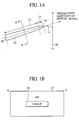
- FIG. 1A and 1B show a structure of the optical coupling element according to the present embodiment.
- FIGs. 2A and 2B are top views of the optical coupling element according to modifications of this embodiment, which show a structure thereof.
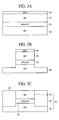
- FIGs. 3A-3C are cross-sectional views of the optical coupling element according to the present embodiment in the steps of the method of fabricating the same.
- FIG 1A is a top view of the optical coupling element according to the present embodiment
- FIG. 1B is a diagrammatic cross-sectional view along the line A-A' in FIG. 1A.
- An optical waveguide 10 for transmitting an optical signal is disposed so that a propagation direction of the optical signal is tilted by an angle ⁇ (e.g., 7° or 10°) to a normal direction of the chip facet 20.
- the first end surface 18 of the optical waveguide 10 is disposed, spaced by a prescribed distance from the chip facet 20, forming a so-called window structure.
- an external optical element such as an optical fiber, optical waveguide, optical lens, optical detector, or other optical device for accepting, transmitting, reflecting, and/or processing the optical signal outputted from optical waveguide 10, or an external optical element (not shown), such as an optical amplifier or other light-generating or amplifying element whose output is optically coupled to optical waveguide 10, is to be provided.
- optical waveguide 10 To the second end surface 16 of the waveguide 10, one or more optical devices (not shown), such as semiconductor optical amplifiers and semiconductor lasers, are to be coupled optically.
- Optical waveguide 10 can be formed by extending an active layer of such optically coupled devices.
- the optical waveguide 10 has a tapered configuration having a width which is decreasing towards the end 18.
- the optical waveguide 10 is divided as shown in FIG. 1A into a basic part 12 and a frontmost end-part (tip) 14.
- the taper of the frontmost end-part 14 is more defined (steeper) than that of the basic part 12.
- the optical waveguide 10 comprises a core layer 38 formed of, e.g., InGaAsP, and a clad layer 42 of InP enclosing the core layer 38.
- the optical coupling element according to the present embodiment has the feature that the optical waveguide 10 is tapered in two stages.
- the respective tapered regions have the following respective functions.
- the taper of the basic part 12 of the optical waveguide 10 is for controlling or improving the optical coupling efficiency to an external optical element.
- the matching is between an optical field transmitting structure and an optical field receiving structure.
- the approximation can be described as the matching of the widths of two optical fields.
- the width of the waveguide end surface 16 of optical waveguide 10, through which a device such as a semiconductor laser or a different optical device is optically connected is determined by the geometrical design of that particular device, obtained from an optical device design procedure to satisfy a predetermined set of functional and optical performance requirements. That is, the taper is for decreasing the width of the optical waveguide 10, which is resulting from the design of the optically coupled device, to a width which results in a generation of a preferred optical spatial field width in a predetermined plane, permitting efficient optical coupling between waveguide 10 and an external optical element.
- the taper of the frontmost end-part 14 of the optical waveguide 10 is for suppressing the residual reflection due to end surface 18.
- the taper of the frontmost end-part 14 must reduce the residual reflection without affecting the desired optical field distribution provided by the basic part 12.
- a sufficiently steep taper is provided in the frontmost end-part 14 in comparison with the taper of the basic part 12.
- a tapered region which is shorter than a length corresponding to 20 wavelengths of the optical signal and which has a width of the end surface 18 of the frontmost end-part 14 less than half the width of the side thereof which is in contact with the basic part 12.
- the length of the frontmost end-part 14 is shorter than a length corresponding to 20 wavelengths of the optical signal, whereby the frontmost end-part 14 does not modify the field profile of the optical signal significantly.
- Such a short taper has little effect on the optical field distribution of the optical signal, and substantially no change in optical coupling efficiency is caused by light passing through the frontmost end-part 14.
- the area of the end surface 18 can be much decreased, whereby the amount of light reflected on the end surface 18 to return to the optical waveguide 10 can be decreased.
- the end surface 18 is not necessarily flat. As exemplified in FIG. 2A, the end surface 18 can be rounded.
- a width of the end surface 18 can be defined as follows. That is, as shown in FIG. 2A, a width of the end surface 18 is defined as the length of a path over end surface 18 between positions p1 and p2 on said surface, where a uniform angle ⁇ is formed concurrently between a vector corresponding to the direction of propagation of an optical signal., a normal vector n(facet) of the chip facet 20 and a normal vector n(p1) at position p1, and a normal vector n(p2) at position p2.
- this width and a width of the side of the frontmost end-part 14 which is in contact with the basic part 12 satisfy the above-described relationship, the effect of the present embodiment can be produced.
- a width of the end surface 18 of the frontmost end-part 14 can be infinitesimally small, i.e., the frontmost end-part 14 may have a triangular top-view shape.
- the optical field distribution of the optical signal is substantially defined by the basic part 12 of the optical waveguide 10, and is not affected by the frontmost end-part 14. Accordingly, even when a width of the end surface 18 tends to zero to thereby suppress a residual reflection, the optical coupling efficiency can be optimized independently.
- both the effective suppression of a residual reflection and an optimum optical coupling efficiency can be realized at once.
- an InGaAsP layer 32 being 200 nm-thick and having a 1.3 ⁇ m-bandgap wavelength equivalent composition, for example, is epitaxially grown on an InP substrate 30 by a MOVPE crystal growth method.
- an InP layer 34 is epitaxially grown on the InGaAsP layer 32 by the same method.
- a silicon dioxide film 36 is formed on the InP layer 34 by a CVD method (FIG. 3A).
- the silicon dioxide film 36 is patterned by lithography and etched into the shape of the optical waveguide 10 as shown in FIG. 1A.
- the InP layer 34 and the InGaAsP layer 32 are dry-etched to form a mesa with a core layer 38 out of the InGaAsP layer 32 (FIG. 3B).
- InP layer 40 is epitaxially grown selectively around said mesa, forming an optical waveguide 10.
- InP layer 40 covers the side surfaces of the core layer 38.
- a core layer 38 of InGaAsP and a clad 42 which is formed by the InP substrate 30 and the InP layers 34 and 40 surrounding the core layer 38, are formed (FIG. 3C).
- optical coupling element shown in FIGs. 1A and 1B can be fabricated.
- An optical coupling element having a 5 ⁇ m-tapered length of the frontmost end-part of the optical waveguide and a 0.8 ⁇ m-width of the end surface was fabricated by the above-described fabrication method.
- An optical coupling element without a frontmost end part would have a residual reflectivity at the end of the optical waveguide, which was reduced by about one order of magnitude in the tapered element.
- a steep tapered region which does not affect the optical coupling efficiency is provided at the end part of the optical waveguide, whereby the effective suppression of a residual reflection and optimization of the optical coupling efficiency can be concurrently realized.
- FIGs. 4 to 6 An optical coupling element according to a second embodiment of the present invention will be explained with reference to FIGs. 4 to 6.
- the same members of the present embodiment as those of the optical coupling element and the method for fabricating the same according to the first embodiment shown in FIGs. 1A-1B, 2A-2B, and 3A-3C are represented by the same reference numbers to simplify their explanation.
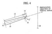
- FIG. 4 is a top view of the optical coupling element according to the present embodiment, which shows a structure thereof.
- FIG. 5 is a contour plot showing a relationship between the width and the angle of an end surface 18 of an optical waveguide 10, and the reflectivity back into waveguide 10 given by simulation.
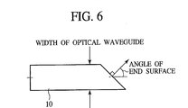
- FIG. 6 is a structure used in the simulation involved in FIG. 5.
- the optical coupling element according to the present embodiment is the same in basic principle as the optical coupling element according to the first embodiment. As shown in FIG. 4, the optical coupling element according to the present embodiment has the feature that a frontmost end-part 14 of an optical waveguide 10 is asymmetrically tapered, and the central axis of the optical waveguide 10 intersects the tapered surface of the optical waveguide 10.
- the frontmost end-part 14 is thus tapered, whereby an angle formed by a normal vector n to the tapered surface which is the end surface 18 and a vector of the propagation direction of the optical signal can be large, such that the residual reflection can be further suppressed.
- an angle formed by a normal vector n on the side surface which is the end surface 18 and a vector aligned with the propagation direction of the optical signal is larger than an angle ⁇ formed by a normal vector to the chip facet 20 and a vector of the propagation direction of the optical signal.
- the reflectivity decreases as a width of the optical waveguide decreases. It is found that at a given width of the optical waveguide, the reflectivity decreases as the angle of the end surface increases. For example, when a width of the optical waveguide is 0.1 ⁇ m, the reflectivity can be decreased by about 2 orders of magnitude when the angle of the end surface is increased to about 15°.
- a frontmost end-part is asymmetrically tapered to make an angle formed by the normal vector of the end surface and a vector aligned with the propagation direction of optical signal large, whereby a residual reflection can be further effectively suppressed.
- FIG. 7 is a top view of the optical device according to the present embodiment, which shows the structure thereof.
- waveguides with active cores and waveguides with passive cores which are both regions for transmitting an optical signal under certain preferred conditions are shown.
- a substrate 50 On a substrate 50 there are formed two distributed feedback semiconductor lasers 52, 54, a combiner 56 which forms laser beams emitted by the distributed feedback lasers 52, 54 into a single coaxial beam, and a semiconductor optical amplifier 58 which amplifies said combined beam from the combiner.
- the optical coupling element 60 according to the second embodiment is connected to the output end of the semiconductor optical amplifier 58.
- Anti-reflection films 62, 64 are formed respectively on the laser end surface and the output coupling end surface of a chip on which these elements are formed.
- An optical fiber 66 is disposed adjacent to the substrate 50 and is optically connected to the optical coupling element 60.
- the optical device which couples and amplifies laser beams emitted by the two distributed feedback semiconductor lasers 52, 54 and outputs the coupled and amplified beams, has the feature that the optical coupling element 60 according to the second embodiment is disposed on the output end of the semiconductor optical amplifier 58.
- optical devices including active elements, such as semiconductor optical amplifiers, semiconductor lasers, etc.
- active elements such as semiconductor optical amplifiers, semiconductor lasers, etc.
- semiconductor optical amplifiers not only is the optical signal amplified but also light reflected on the end surface is amplified which resultantly often causes ripples in the wavelength dependency of the optical gain. Accordingly, it is more necessary for optical amplifiers of higher amplification factors to suppress the reflection on the end surface.
- the optical coupling element 60 according to the second embodiment is disposed on the output end of the semiconductor optical amplifier 58, whereby the reflection near the chip facet is effectively suppressed. Accordingly, the optical device can have high performance.
- the distributed feedback semiconductor lasers 52, 54, the combiner 56 and the semiconductor optical amplifier 58 can respectively have known structures.
- the anti-reflection films 62, 64 can be formed of, for example 270 nm-thick silicon dioxide films.
- the optical coupling element 60 is a part of the semiconductor optical amplifier 58.
- the optical coupling element according to the second embodiment is disposed on the output end of the optical device, whereby the optical device can have little residual reflection and high performance.
- FIG. 8 is a top view of the optical device according to the present embodiment, which shows its structure.
- waveguides with active cores and waveguides with passive cores which are both regions for transmitting an optical signal under certain preferred conditions are shown.
- a semiconductor optical amplifier 58 is formed on a substrate 50.
- the optical coupling elements 60a, 60b according to the second embodiment are disposed respectively on a first coupling end and on a second coupling end of said semiconductor optical amplifier.
- Anti-reflection films 62, 64 are formed on the respective first end surface and second end surface of the chip where said semiconductor optical amplifier 58 is formed on.
- Optical fibers 66a and 66b are disposed adjacent to the substrate 50 and are optically connected to the optical coupling elements 60a and 60b, respectively.
- the optical device which amplifies an incident optical signal on said first end of the semiconductor optical amplifier 58 and outputs the amplified optical signal on said second end, has the feature that the optical coupling elements 60 according to the second embodiment are disposed respectively on said first end and said second end of the semiconductor optical amplifier 58.
- the optical coupling element according to the second embodiment is disposed on the input end as well, whereby the reflection at the output end surface can be effectively suppressed, and the re-reflection of the reflected light on the input end surface can be also suppressed. Accordingly, the optical device can have high performance.
- the optical coupling elements are a part of the semiconductor optical amplifier 58.
- the entire waveguide may be fabricated with an active waveguide core.
- the optical coupling elements according to the second embodiment are disposed respectively on the input end and the output end of the optical device, whereby the optical device can have little residual reflection and have high performance.
- anti-reflection film is provided on the chip facet in the first and the second embodiments, but anti-reflection films may be provided.
- a window structure is provided on the output end of the optical waveguide but is not essential. As long as the reflection on the chip facet is insignificant or can be sufficiently suppressed by anti-reflection film or other means, the window structure may not be provided. Similarly, the optical waveguide may be arranged so that a propagation direction of optical signal is not tilted from a normal direction of the chip facet.
- the reflected light causing a residual reflection contains light reflected at the chip facet, and light reflected at the end surface of the optical waveguide.
- the present invention aims at suppressing the reflection mainly at the optical waveguide end surface and preventing this light from coupling back into the waveguide.
- the anti-reflection film, the window structure and the tilted structure of the optical waveguide aim at suppressing reflections mainly at the chip facet and the entering of reflected light into the optical waveguide. Accordingly, without using them, the structure of the present invention can suppress the reflection on the end surface of the optical waveguide. In terms of generally suppressing reflections, it is preferable to combine these structures.
- the optical coupling elements have two stages of tapers which linearly change the widths of the optical waveguides.
- the two-stage taper which linearly changes the widths of the optical waveguides, is not essential.
- the frontmost end-part may be rounded, and in this case as well, a width of the frontmost end-part can be defined as in FIG. 2A.
- laser beams emitted by the two distributed feedback semiconductor lasers are coupled and amplified to output the amplified laser beam
- incident light is amplified by the semiconductor optical amplifier to output the amplified light.
- Optical devices the present invention can be applied to are not limited to the embodiments described above.
- the present invention is applicable widely to optical devices having a structure for optically connecting the optical element to the optical transmitting element, such as optical fibers, etc.
- optical amplifier in the claims extends to any kind of active element for generating or altering an optical signal.
- the optical coupling element according to the second embodiment is used, but the optical coupling element according to the first embodiment shown in FIGs. 1A, 2A or 2B may be used alternatively.
- optical coupling elements having the same structure are provided on the input end and the output end of the semiconductor optical amplifier 58, but the optical coupling elements on the input end and the output end may have structures different from each other.
- Materials forming the optical coupling element are not limited to the material groups described in the above-described embodiments and can be suitably selected out of suitable material groups, based on wavelengths of optical signal, etc.
- wavelengths of optical light with which the present invention may be used include 1300nm to 1650nm.
- the invention need not be limited solely to optical frequencies, but could be applied to other frequencies from the electromagnetic spectrum suitable for putting the invention into operation.
Landscapes
- Physics & Mathematics (AREA)
- Engineering & Computer Science (AREA)
- General Physics & Mathematics (AREA)
- Optics & Photonics (AREA)
- Power Engineering (AREA)
- Microelectronics & Electronic Packaging (AREA)
- Optical Integrated Circuits (AREA)
Abstract
Description
- The present invention relates to an optical coupling element and an optical device, more specifically an optical coupling element which can effectively prevent residual reflection without sacrificing optical coupling efficiency, and an optical device comprising the optical coupling element.
- It is known that internal residual reflections of optical signal in optical devices are a factor degrading device performance. For example, in laser oscillators, when residually reflected light returns into the oscillator, the residually reflected light disturbs oscillation states, and this interference increases noise components. A method able to suppress the generation of the residually reflected light in the optical coupling elements is thus very important.
- Usually the most important source of reflections is the device structure (coupling element) used to couple optical power (light waves) in and out of the chip on which the optical device or the optical integrated circuit is located. These structures have regions where the devices contact the atmosphere, and due to a large refractive index difference between material forming the devices and air, light rays are reflected at the interface therebetween to become residual reflection light.
- Recently, methods for preventing the residual reflection, for example the following methods, have been proposed.
- In a first method, an anti-reflection film is formed on the chip facet. This method can reduce the reflectivity of the chip facet.
- In a second method, the optical waveguide is tilted by a prescribed angle (e.g., about 7°) relative to a normal vector on the chip facet. This method can decrease the amount of light reflected at the chip facet and coupled back into the optical waveguide.
- In a third method, the width of the optical waveguide is tapered toward the output end. This method widens the effective optical field distribution at the chip facet, whereby the amount of light reflected at the chip facet and coupled back into the optical waveguide can be decreased, and also the optical field-width of the optical power can be easily matched with the optical field-width of the optical propagation element optically coupled to the output end of the optical waveguide.
- In a fourth method, a so-called window structure is used. A window structure is a structure in which the end of the optical waveguide is spaced from the chip facet. In cases using the window structure, the optical field width of the optical power outputted from the end of the optical waveguide increases gradually in the direction of propagation of the optical power. Accordingly, this method can reduce the amount of light reflected at the chip facet and coupled back into the optical waveguide.
- These methods are used separately, or in combinations of two or more.
- FIG. 9A is a top view of the structure of an optical coupling element using the second to fourth methods described above. That is, in the optical coupling element of FIG. 9A, the
optical waveguide 100 is tapered so as to have a smaller width at theoutput end surface 104 than at theinput end surface 102, a window region is provided between theoutput end surface 104 and thechip facet 110, and theoptical waveguide 100 is arranged so that a propagation direction of the optical signal on the chip has a prescribed tilt angle to a normal vector on thechip facet 110. The optical coupling element of FIG. 9A can effectively prevent light reflected at thechip facet 110 from returning into theoptical waveguide 100. - On the other hand, in the optical coupling element, it is very important not only to prevent residual reflection near the chip facet but also to increase optical coupling efficiency between the optical waveguide formed on the chip and external optical elements, such as optical fibers, etc. formed outside the chip. To this end, an end configuration of the end of the optical waveguide, e.g. the length of the tapered region and the width of the end surface, is optimized by simulation tools so as to obtain good optical coupling efficiency.
- The optical coupling element shown in FIG. 9A has a structure which is very effective at preventing reflected light from the
chip facet 110 from returning into theoptical waveguide 100. However, it cannot be said that the structure is sufficient for suppressing residual reflection. That is, as shown in FIG. 9B, light is internally reflected at the output end surface of theoptical waveguide 100 inside the chip, but the optical coupling element shown in FIG. 9A does not address this reflection at theoutput end surface 104 of theoptical waveguide 100 and cannot suppress the generation of the residual reflection light due to this reflection at theoutput end surface 104. - In order to suppress the reflection at the output end surface of the optical waveguide, it has been considered to taper the optical waveguide so that the optical waveguide has a zero-width at the end surface of the optical waveguide. However, an optimum value of the optical coupling efficiency can be obtained in a tapered structure, in which the end surface has a prescribed non-zero width. Accordingly, the tapered structure, in which the end surface of an optical waveguide has a zero-width, has lower optical coupling efficiency in comparison with the tapered structure, in which the end surface has a prescribed non-zero width. In terms of fabrication, it is very difficult to form with good reproducibility an optical waveguide having a zero-width end surface and the end thereof accurately aligned.
- It is therefore desirable to provide an optical coupling element which can effectively prevent residual reflection without sacrificing optical coupling efficiencies, and an optical device comprising one or more optical coupling elements.
- According to one aspect of the present invention, there is provided an optical coupling element for propagating an optical signal by optically coupling an optical element formed on a substrate to an external optical element disposed adjacent to the substrate, comprising: a first optical waveguide formed on the substrate and having a width of a first side surface smaller than a width of a second side surface; and a second optical waveguide formed on the substrate and connected to the first side of the first optical waveguide at a first end surface, having a width of a second end surface smaller than a width of the said first end surface, and having a shorter length than a length corresponding to 20 wavelengths of the optical signal.
- According to another aspect of the present invention, there is provided an optical device acting upon an optical signal, comprising: an optical amplifier formed on a substrate; and an optical coupling element formed on the substrate and optically connected to one end of the optical amplifier, the optical coupling element including: a first optical waveguide connected at one end surface to the optical amplifier, and having a width on the other end surface smaller than a width on said one surface; and a second optical waveguide connected at a first end surface to said other end surface of the first optical waveguide, having a width on a second end surface smaller than a width on said first end surface, and having a shorter length than a length corresponding to 20 wavelengths of the optical signal.
- According to another aspect of the present invention, there is provided an optical device acting upon an optical signal and comprising: an optical amplifier formed on a substrate; a first optical coupling element formed on the substrate and optically connected to one end of the optical amplifier; and a second optical coupling element formed on the substrate and optically connected to another end of the optical amplifier, each of the first optical coupling element and the second optical coupling element including: a first optical waveguide connected at one end surface to the optical amplifier, and having a width on the other end surface smaller than a width on said one surface; and a second optical waveguide connected at a first end surface to said other end surface of the first optical waveguide, having a width on a second end surface smaller than a width on said first end surface, and having a shorter length than a length corresponding to 20 wavelengths of the optical signal.
- According to another aspect of the present invention, there is provided an optical device acting upon an optical signal and comprising: an optical amplifier formed on a substrate; an optical coupling element formed on the substrate and optically connected to the optical amplifier, and an external optical element disposed adjacent to the substrate and optically connected to the optical coupling element, the optical coupling element including: a first optical waveguide having a width on a first side towards the external optical element smaller than a width on a second side connected to the optical amplifier; and a second optical waveguide connected to the said first side of the first optical waveguide at a first end, and having a width of a second end towards the external optical element smaller than a width of the first end and having a shorter length than a length corresponding to 20 wavelengths of the optical signal.
- According to another aspect of the present invention, there is provided an optical device acting upon an optical signal and comprising: an optical amplifier formed on a substrate; a first optical coupling element formed on the substrate and optically connected to one end of the optical amplifier; a second optical coupling element formed on the substrate and optically connected to another end of the optical amplifier; a first external optical element disposed adjacent to the substrate and optically connected to the first optical coupling element; and a second external optical element disposed adjacent to the substrate and optically connected to the second optical coupling element, each of the first optical coupling element and the second optical coupling element including: a first optical waveguide having a width on a first side towards the external optical element smaller than a width on a second side connected to the optical amplifier; and a second optical waveguide connected to the first side of the first optical waveguide at a first end, and having a width of a second end towards the external optical element smaller than a width of the first end and having a shorter length than a length corresponding to 20 wavelengths of the optical signal.
- As described above, according to the present invention, the optical waveguide optically connected to an optical device includes a basic part, and a frontmost end-part, having tapers different from each other, so that the basic part increases optical coupling efficiency, and the frontmost end-part suppresses the residual reflection, whereby the effective suppression of the residual reflection and the optimization of the optical coupling efficiency can be concurrently realized.
- Reference is made, by way of example only, to the accompanying drawings in which:
- FIG. 1A is a top view of an optical coupling element according to the first embodiment of the present invention, and shows the structure thereof.
- FIG. 1B is a diagrammatic cross-sectional view of the optical coupling element according to the first embodiment of the present invention, which shows the structure thereof.
- FIGs. 2A and 2B are top views of the optical coupling element according to modifications of the first embodiment of the present invention, which show the structure thereof.
- FIGs. 3A-3C are cross-sectional views of the optical coupling element according to the first embodiment of the present invention at different stages of fabrication of the same.
- FIG. 4 is a top view of an optical coupling element according to a second embodiment of the present invention, and shows the structure thereof.
- FIG. 5 is a graph of relationships between the width and the angle of the end surface of the optical waveguide, and the reflectivity given by simulation.
- FIG. 6 shows the structure used in the simulation involved in FIG. 5.
- FIG. 7 is a top view of an optical device according to a third embodiment of the present invention, and shows the structure thereof.
- FIG. 8 is a top view of an optical device according to a fourth embodiment of the present invention, and shows the structure thereof.
- FIGs. 9A and 9B show a previously-proposed optical coupling element, and show its structure and associated problems.
- An optical coupling element according to a first embodiment of the present invention will be explained with reference to FIGs. 1A-1B, 2A-2B and 3A-3C.
- FIG. 1A and 1B show a structure of the optical coupling element according to the present embodiment. FIGs. 2A and 2B are top views of the optical coupling element according to modifications of this embodiment, which show a structure thereof. FIGs. 3A-3C are cross-sectional views of the optical coupling element according to the present embodiment in the steps of the method of fabricating the same.
- First, the structure of the optical coupling element according to the present embodiment will be explained with reference to FIGs. 1A-1B and 2A-2B. FIG 1A is a top view of the optical coupling element according to the present embodiment, and FIG. 1B is a diagrammatic cross-sectional view along the line A-A' in FIG. 1A.
- An
optical waveguide 10 for transmitting an optical signal is disposed so that a propagation direction of the optical signal is tilted by an angle α (e.g., 7° or 10°) to a normal direction of thechip facet 20. Thefirst end surface 18 of theoptical waveguide 10 is disposed, spaced by a prescribed distance from thechip facet 20, forming a so-called window structure. Next to thechip facet 20, an external optical element (not shown), such as an optical fiber, optical waveguide, optical lens, optical detector, or other optical device for accepting, transmitting, reflecting, and/or processing the optical signal outputted fromoptical waveguide 10, or an external optical element (not shown), such as an optical amplifier or other light-generating or amplifying element whose output is optically coupled tooptical waveguide 10, is to be provided. - To the
second end surface 16 of thewaveguide 10, one or more optical devices (not shown), such as semiconductor optical amplifiers and semiconductor lasers, are to be coupled optically.Optical waveguide 10 can be formed by extending an active layer of such optically coupled devices. - As shown in FIG. 1A, the
optical waveguide 10 has a tapered configuration having a width which is decreasing towards theend 18. For explanation, theoptical waveguide 10 is divided as shown in FIG. 1A into abasic part 12 and a frontmost end-part (tip) 14. The taper of the frontmost end-part 14 is more defined (steeper) than that of thebasic part 12. As shown in FIG. 1B, theoptical waveguide 10 comprises acore layer 38 formed of, e.g., InGaAsP, and aclad layer 42 of InP enclosing thecore layer 38. - As described above, the optical coupling element according to the present embodiment has the feature that the
optical waveguide 10 is tapered in two stages. The respective tapered regions have the following respective functions. - The taper of the
basic part 12 of theoptical waveguide 10 is for controlling or improving the optical coupling efficiency to an external optical element. To increase the optical coupling efficiency to the external optical element optically connected tooptical waveguide 10 through thewaveguide end surface 18 of saidoptical waveguide 10, it is necessary to approximate (match) as closely as possible the optical spatial field characteristics at a predetermined surface, depending on the nature of the optical characteristics of the external optical element. Typically the matching is between an optical field transmitting structure and an optical field receiving structure. Typically the approximation can be described as the matching of the widths of two optical fields. - On the other hand, the width of the
waveguide end surface 16 ofoptical waveguide 10, through which a device such as a semiconductor laser or a different optical device is optically connected, is determined by the geometrical design of that particular device, obtained from an optical device design procedure to satisfy a predetermined set of functional and optical performance requirements. That is, the taper is for decreasing the width of theoptical waveguide 10, which is resulting from the design of the optically coupled device, to a width which results in a generation of a preferred optical spatial field width in a predetermined plane, permitting efficient optical coupling betweenwaveguide 10 and an external optical element. - The taper of the frontmost end-
part 14 of theoptical waveguide 10 is for suppressing the residual reflection due to endsurface 18. The taper of the frontmost end-part 14 must reduce the residual reflection without affecting the desired optical field distribution provided by thebasic part 12. In the optical coupling element according to the present embodiment, a sufficiently steep taper is provided in the frontmost end-part 14 in comparison with the taper of thebasic part 12. To be specific, a tapered region which is shorter than a length corresponding to 20 wavelengths of the optical signal and which has a width of theend surface 18 of the frontmost end-part 14 less than half the width of the side thereof which is in contact with thebasic part 12. The length of the frontmost end-part 14 is shorter than a length corresponding to 20 wavelengths of the optical signal, whereby the frontmost end-part 14 does not modify the field profile of the optical signal significantly. - Such a short taper has little effect on the optical field distribution of the optical signal, and substantially no change in optical coupling efficiency is caused by light passing through the frontmost end-
part 14. The area of theend surface 18 can be much decreased, whereby the amount of light reflected on theend surface 18 to return to theoptical waveguide 10 can be decreased. - The
end surface 18 is not necessarily flat. As exemplified in FIG. 2A, theend surface 18 can be rounded. In this case, a width of theend surface 18 can be defined as follows. That is, as shown in FIG. 2A, a width of theend surface 18 is defined as the length of a path overend surface 18 between positions p1 and p2 on said surface, where a uniform angle α is formed concurrently between a vector corresponding to the direction of propagation of an optical signal., a normal vector n(facet) of thechip facet 20 and a normal vector n(p1) at position p1, and a normal vector n(p2) at position p2. When this width and a width of the side of the frontmost end-part 14 which is in contact with thebasic part 12 satisfy the above-described relationship, the effect of the present embodiment can be produced. - Otherwise, as exemplified in FIG. 2B, a width of the
end surface 18 of the frontmost end-part 14 can be infinitesimally small, i.e., the frontmost end-part 14 may have a triangular top-view shape. The optical field distribution of the optical signal is substantially defined by thebasic part 12 of theoptical waveguide 10, and is not affected by the frontmost end-part 14. Accordingly, even when a width of theend surface 18 tends to zero to thereby suppress a residual reflection, the optical coupling efficiency can be optimized independently. - According to the optical coupling element of the present embodiment, both the effective suppression of a residual reflection and an optimum optical coupling efficiency can be realized at once.
- An example of a preferred method for fabricating the optical coupling element according to the present embodiment will be explained with reference to FIGs. 3A-3C.
- First, an
InGaAsP layer 32 being 200 nm-thick and having a 1.3 µm-bandgap wavelength equivalent composition, for example, is epitaxially grown on anInP substrate 30 by a MOVPE crystal growth method. - Then, an
InP layer 34 is epitaxially grown on theInGaAsP layer 32 by the same method. - Next, a
silicon dioxide film 36 is formed on theInP layer 34 by a CVD method (FIG. 3A). - Next, the
silicon dioxide film 36 is patterned by lithography and etched into the shape of theoptical waveguide 10 as shown in FIG. 1A. - Next, with the patterned
silicon dioxide film 36 as a mask, theInP layer 34 and theInGaAsP layer 32 are dry-etched to form a mesa with acore layer 38 out of the InGaAsP layer 32 (FIG. 3B). - Then, an
InP layer 40 is epitaxially grown selectively around said mesa, forming anoptical waveguide 10.InP layer 40 covers the side surfaces of thecore layer 38. - Next, the silicon dioxide film is removed, and another InP layer is grown to make the surface flat. Thus, a
core layer 38 of InGaAsP and a clad 42, which is formed by theInP substrate 30 and the InP layers 34 and 40 surrounding thecore layer 38, are formed (FIG. 3C). - Thus, the optical coupling element shown in FIGs. 1A and 1B can be fabricated.
- An optical coupling element having a 5 µm-tapered length of the frontmost end-part of the optical waveguide and a 0.8 µm-width of the end surface was fabricated by the above-described fabrication method. An optical coupling element without a frontmost end part would have a residual reflectivity at the end of the optical waveguide, which was reduced by about one order of magnitude in the tapered element.
- As described above, according to the present embodiment, a steep tapered region which does not affect the optical coupling efficiency is provided at the end part of the optical waveguide, whereby the effective suppression of a residual reflection and optimization of the optical coupling efficiency can be concurrently realized.
- An optical coupling element according to a second embodiment of the present invention will be explained with reference to FIGs. 4 to 6. The same members of the present embodiment as those of the optical coupling element and the method for fabricating the same according to the first embodiment shown in FIGs. 1A-1B, 2A-2B, and 3A-3C are represented by the same reference numbers to simplify their explanation.
- FIG. 4 is a top view of the optical coupling element according to the present embodiment, which shows a structure thereof. FIG. 5 is a contour plot showing a relationship between the width and the angle of an
end surface 18 of anoptical waveguide 10, and the reflectivity back intowaveguide 10 given by simulation. FIG. 6 is a structure used in the simulation involved in FIG. 5. - The optical coupling element according to the present embodiment is the same in basic principle as the optical coupling element according to the first embodiment. As shown in FIG. 4, the optical coupling element according to the present embodiment has the feature that a frontmost end-
part 14 of anoptical waveguide 10 is asymmetrically tapered, and the central axis of theoptical waveguide 10 intersects the tapered surface of theoptical waveguide 10. - The frontmost end-
part 14 is thus tapered, whereby an angle formed by a normal vector n to the tapered surface which is theend surface 18 and a vector of the propagation direction of the optical signal can be large, such that the residual reflection can be further suppressed. - To be more specific, it is preferable that an angle formed by a normal vector n on the side surface which is the
end surface 18 and a vector aligned with the propagation direction of the optical signal is larger than an angle α formed by a normal vector to thechip facet 20 and a vector of the propagation direction of the optical signal. The frontmost end-part is thus tapered, whereby the residual reflection can be effectively suppressed. - As shown by FIG. 5, it is found that at a given angle of the end surface (the angle between a normal vector and the propagation direction) the reflectivity decreases as a width of the optical waveguide decreases. It is found that at a given width of the optical waveguide, the reflectivity decreases as the angle of the end surface increases. For example, when a width of the optical waveguide is 0.1 µm, the reflectivity can be decreased by about 2 orders of magnitude when the angle of the end surface is increased to about 15°.
- As described above, according to the present embodiment, a frontmost end-part is asymmetrically tapered to make an angle formed by the normal vector of the end surface and a vector aligned with the propagation direction of optical signal large, whereby a residual reflection can be further effectively suppressed.
- An optical device according to a third embodiment of the present invention will be explained with reference to FIG. 7.
- FIG. 7 is a top view of the optical device according to the present embodiment, which shows the structure thereof. In FIG. 7 waveguides with active cores and waveguides with passive cores which are both regions for transmitting an optical signal under certain preferred conditions are shown.
- On a
substrate 50 there are formed two distributedfeedback semiconductor lasers combiner 56 which forms laser beams emitted by the distributedfeedback lasers optical amplifier 58 which amplifies said combined beam from the combiner. Theoptical coupling element 60 according to the second embodiment is connected to the output end of the semiconductoroptical amplifier 58.Anti-reflection films optical fiber 66 is disposed adjacent to thesubstrate 50 and is optically connected to theoptical coupling element 60. - As described above, the optical device according to the present embodiment, which couples and amplifies laser beams emitted by the two distributed
feedback semiconductor lasers optical coupling element 60 according to the second embodiment is disposed on the output end of the semiconductoroptical amplifier 58. - For optical devices including active elements, such as semiconductor optical amplifiers, semiconductor lasers, etc., it is especially important to suppress reflectivities near the chip facet. In semiconductor optical amplifiers, not only is the optical signal amplified but also light reflected on the end surface is amplified which resultantly often causes ripples in the wavelength dependency of the optical gain. Accordingly, it is more necessary for optical amplifiers of higher amplification factors to suppress the reflection on the end surface.
- In the optical device according to the present embodiment, the
optical coupling element 60 according to the second embodiment is disposed on the output end of the semiconductoroptical amplifier 58, whereby the reflection near the chip facet is effectively suppressed. Accordingly, the optical device can have high performance. - The distributed
feedback semiconductor lasers combiner 56 and the semiconductoroptical amplifier 58 can respectively have known structures. Theanti-reflection films - In the optical device according to the present embodiment, it is possible that the
optical coupling element 60 is a part of the semiconductoroptical amplifier 58. - As described above, according to the present embodiment, the optical coupling element according to the second embodiment is disposed on the output end of the optical device, whereby the optical device can have little residual reflection and high performance.
- An optical device according to a fourth embodiment of the present invention will be explained with reference to FIG. 8.
- FIG. 8 is a top view of the optical device according to the present embodiment, which shows its structure. In FIG. 8, waveguides with active cores and waveguides with passive cores which are both regions for transmitting an optical signal under certain preferred conditions are shown.
- A semiconductor
optical amplifier 58 is formed on asubstrate 50. Theoptical coupling elements Anti-reflection films optical amplifier 58 is formed on.Optical fibers substrate 50 and are optically connected to theoptical coupling elements - As described above, the optical device according to the present embodiment, which amplifies an incident optical signal on said first end of the semiconductor
optical amplifier 58 and outputs the amplified optical signal on said second end, has the feature that theoptical coupling elements 60 according to the second embodiment are disposed respectively on said first end and said second end of the semiconductoroptical amplifier 58. The optical coupling element according to the second embodiment is disposed on the input end as well, whereby the reflection at the output end surface can be effectively suppressed, and the re-reflection of the reflected light on the input end surface can be also suppressed. Accordingly, the optical device can have high performance. - In the optical device according to the present embodiment, it is possible that the optical coupling elements are a part of the semiconductor
optical amplifier 58. Alternatively, the entire waveguide may be fabricated with an active waveguide core. - As described above, according to the present embodiment, the optical coupling elements according to the second embodiment are disposed respectively on the input end and the output end of the optical device, whereby the optical device can have little residual reflection and have high performance.
- The present invention is not limited to the above-described embodiments and can cover various modifications.
- For example, no anti-reflection film is provided on the chip facet in the first and the second embodiments, but anti-reflection films may be provided.
- In the first to the fourth embodiments, a window structure is provided on the output end of the optical waveguide but is not essential. As long as the reflection on the chip facet is insignificant or can be sufficiently suppressed by anti-reflection film or other means, the window structure may not be provided. Similarly, the optical waveguide may be arranged so that a propagation direction of optical signal is not tilted from a normal direction of the chip facet.
- The reflected light causing a residual reflection contains light reflected at the chip facet, and light reflected at the end surface of the optical waveguide. However, the present invention aims at suppressing the reflection mainly at the optical waveguide end surface and preventing this light from coupling back into the waveguide. On the other hand, the anti-reflection film, the window structure and the tilted structure of the optical waveguide aim at suppressing reflections mainly at the chip facet and the entering of reflected light into the optical waveguide. Accordingly, without using them, the structure of the present invention can suppress the reflection on the end surface of the optical waveguide. In terms of generally suppressing reflections, it is preferable to combine these structures.
- In the first and the second embodiments, the optical coupling elements have two stages of tapers which linearly change the widths of the optical waveguides. However, the two-stage taper, which linearly changes the widths of the optical waveguides, is not essential. For example, in place of providing the steep tapered region on the frontmost end-part, the frontmost end-part may be rounded, and in this case as well, a width of the frontmost end-part can be defined as in FIG. 2A.
- In the third embodiment, laser beams emitted by the two distributed feedback semiconductor lasers are coupled and amplified to output the amplified laser beam, and in the fourth embodiment, incident light is amplified by the semiconductor optical amplifier to output the amplified light. Optical devices the present invention can be applied to are not limited to the embodiments described above. The present invention is applicable widely to optical devices having a structure for optically connecting the optical element to the optical transmitting element, such as optical fibers, etc. Thus, the term "optical amplifier" in the claims extends to any kind of active element for generating or altering an optical signal.
- In the third and the fourth embodiments, the optical coupling element according to the second embodiment is used, but the optical coupling element according to the first embodiment shown in FIGs. 1A, 2A or 2B may be used alternatively.
- In the fourth embodiment, optical coupling elements having the same structure are provided on the input end and the output end of the semiconductor
optical amplifier 58, but the optical coupling elements on the input end and the output end may have structures different from each other. - Materials forming the optical coupling element are not limited to the material groups described in the above-described embodiments and can be suitably selected out of suitable material groups, based on wavelengths of optical signal, etc.
- Examples of wavelengths of optical light with which the present invention may be used include 1300nm to 1650nm. However, the invention need not be limited solely to optical frequencies, but could be applied to other frequencies from the electromagnetic spectrum suitable for putting the invention into operation.
Claims (17)
- An optical coupling element for propagating an optical signal by optically coupling an optical element formed on a substrate to an external optical element disposed adjacent to the substrate, comprising:a first optical waveguide formed on the substrate and having a width of a first side surface smaller than a width of a second side surface; anda second optical waveguide formed on the substrate and connected to the first side of the first optical waveguide at a first end surface, and having a width of a second end surface smaller than a width of the said first end surface, and having a shorter length than a length corresponding to 20 wavelengths of the optical signal.
- An optical coupling element according to claim 1, wherein
the width of the first optical waveguide is linearly tapered toward the first side surface to a first degree; and
the width of the second optical waveguide is linearly tapered toward the second end surface to a second degree, steeper than the first degree. - An optical coupling element according to claim 1 or 2, wherein
the width of the second optical waveguide at the second end surface is less than half of the width of the second optical waveguide at the first end surface. - An optical coupling element according to any preceding claim, wherein
an optical field distribution of the optical signal propagating through the second optical waveguide is substantially constant in shape over the second optical wave guide between the second end surface on the side of the external optical element and the first end surface on the side of the optical element. - An optical coupling element according to any preceding claim, wherein
the first optical waveguide transforms an optical field distribution so that an optical field width of the optical signal outputted from the optical element is substantially equal to an optical field width of optimum acceptance of the external optical element. - An optical coupling element according to any of claims 1 to 4, wherein
the first optical waveguide transforms an optical field distribution so that an optical field width of the optical signal outputted from the external optical element is substantially equal to an optical field width of optimum acceptance of the optical element. - An optical coupling element according to any preceding claim, wherein
the second optical waveguide is formed in substantially triangular shape in at least one plane. - An optical coupling element according to claim 1, wherein
side surfaces of the second optical waveguide are tapered asymmetrically to a propagation direction of the optical signal, and the propagation direction of the optical signal intersects one of the side surfaces. - An optical coupling element according to claim 1, wherein
the second optical waveguide has a second end surface on the side of the external optical element that is rounded. - An optical coupling element according to any preceding claim, arranged wherein
a propagation direction of the signal light propagating through the optical coupling element and a normal vector of a facet of the substrate form a prescribed angle larger than 0°. - An optical coupling element according to claim 10, wherein
an angle formed by a normal vector to the second end surface of the second optical waveguide for the optical signal propagating through and the normal vector to the end surface of the substrate is larger than the said prescribed angle. - An optical coupling element according to any preceding claim, wherein
an end surface of the second optical waveguide on the side of the external optical element is spaced from an end surface of the substrate. - An optical coupling element according to any preceding claim, further comprising:an anti-reflection film formed on an end surface of the substrate.
- An optical device acting upon an optical signal and comprising:an optical amplifier formed on a substrate; andan optical coupling element formed on the substrate and optically connected to one end of the optical amplifier,the optical coupling element including: a first optical waveguide connected at one end surface to the optical amplifier, and having a width on the other end surface smaller than a width on said one surface; and a second optical waveguide connected at a first end surface to said other end surface of the first optical waveguide, having a width on a second end surface smaller than a width on said first end surface, and having a shorter length than a length corresponding to 20 wavelengths of the optical signal.
- An optical device acting upon an optical signal and comprising:an optical amplifier formed on a substrate;a first optical coupling element formed on the substrate and optically connected to one end of the optical amplifier; anda second optical coupling element formed on the substrate and optically connected to another end of the optical amplifier,each of the first optical coupling element and the second optical coupling element including: a first optical waveguide connected at one end surface to the optical amplifier, and having a width on the other end surface smaller than a width on said one surface; and a second optical waveguide connected at a first end surface to said other end surface of the first optical waveguide, having a width on a second end surface smaller than a width on said first end surface, and having a shorter length than a length corresponding to 20 wavelengths of the optical signal.
- An optical device acting upon an optical signal and comprising:an optical amplifier formed on a substrate;an optical coupling element formed on the substrate and optically connected to the optical amplifier, andan external optical element disposed adjacent to the substrate and optically connected to the optical coupling element,the optical coupling element including: a first optical waveguide having a width on a first side towards the external optical element smaller than a width on a second side connected to the optical amplifier; and a second optical waveguide connected to the first side of the first optical waveguide at a first end, and having a width of a second end towards the external optical element smaller than a width of the first end and having a shorter length than a length corresponding to 20 wavelengths of the optical signal.
- An optical device acting upon an optical signal and comprising:an optical amplifier formed on a substrate;a first optical coupling element formed on the substrate and optically connected to one end of the optical amplifier;a second optical coupling element formed on the substrate and optically connected to another end of the optical amplifier;a first external optical element disposed adjacent to the substrate and optically connected to the first optical coupling element; anda second external optical element disposed adjacent to the substrate and optically connected to the second optical coupling element,each of the first optical coupling element and the second optical coupling element including: a first optical waveguide having a width on a first side towards the external optical element smaller than a width on a second side connected to the optical amplifier; and a second optical waveguide connected to the first side of the first optical waveguide at a first end, and having a width of a second end towards the external optical element smaller than a width of the first end and having a shorter length than a length corresponding to 20 wavelengths of the optical signal.
Applications Claiming Priority (2)
| Application Number | Priority Date | Filing Date | Title |
|---|---|---|---|
| JP2002057301A JP3766637B2 (en) | 2002-03-04 | 2002-03-04 | Optical coupling element and optical device |
| JP2002057301 | 2002-03-04 |
Publications (2)
| Publication Number | Publication Date |
|---|---|
| EP1343028A1 true EP1343028A1 (en) | 2003-09-10 |
| EP1343028B1 EP1343028B1 (en) | 2005-12-14 |
Family
ID=27751034
Family Applications (1)
| Application Number | Title | Priority Date | Filing Date |
|---|---|---|---|
| EP03250989A Expired - Lifetime EP1343028B1 (en) | 2002-03-04 | 2003-02-18 | Integrated mode size adapter optical waveguide with reduced back-reflection |
Country Status (4)
| Country | Link |
|---|---|
| US (1) | US7046880B2 (en) |
| EP (1) | EP1343028B1 (en) |
| JP (1) | JP3766637B2 (en) |
| DE (1) | DE60302684T2 (en) |
Families Citing this family (10)
| Publication number | Priority date | Publication date | Assignee | Title |
|---|---|---|---|---|
| US7203409B2 (en) * | 2004-08-16 | 2007-04-10 | Covega Corporation | Superluminescent diodes having high output power and reduced internal reflections |
| SE0850021L (en) * | 2008-09-23 | 2009-12-29 | Syntune Ab | Waveguide for low reflex switch-off. |
| JP2012048036A (en) * | 2010-08-27 | 2012-03-08 | Fujikura Ltd | Optical waveguide element |
| JP6303280B2 (en) * | 2013-04-05 | 2018-04-04 | 三菱電機株式会社 | Optical waveguide and integrated optical device |
| US20160377809A1 (en) * | 2015-06-25 | 2016-12-29 | Futurewei Technologies, Inc. | Optical Edge Coupling With A Separate Trimmed Taper |
| US10545291B1 (en) * | 2018-08-28 | 2020-01-28 | Cisco Technology, Inc. | Gain integration in Si photonic coherent modulators |
| JP7379962B2 (en) | 2019-09-04 | 2023-11-15 | 株式会社デンソー | Optical waveguide termination element and optical filter using it |
| US12405420B2 (en) | 2021-09-23 | 2025-09-02 | Apple Inc. | Light output devices and light outputting methods for optical systems |
| US12292597B2 (en) | 2021-09-23 | 2025-05-06 | Apple Inc. | Light output devices and light outputting methods for optical systems |
| JP2024535074A (en) * | 2021-09-23 | 2024-09-26 | アップル インコーポレイテッド | Light output device and method for optical system - Patents.com |
Citations (3)
| Publication number | Priority date | Publication date | Assignee | Title |
|---|---|---|---|---|
| US5737352A (en) * | 1995-11-08 | 1998-04-07 | U.S. Philips Corporation | Semiconductor diode laser, in particular a laser amplifier, and method of manufacturing this laser |
| GB2326020A (en) * | 1997-06-06 | 1998-12-09 | Ericsson Telefon Ab L M | Coupling a semiconductor device to an optical fibre |
| WO1999066613A1 (en) * | 1998-06-16 | 1999-12-23 | Sarnoff Corporation | High power semiconductor light source |
Family Cites Families (4)
| Publication number | Priority date | Publication date | Assignee | Title |
|---|---|---|---|---|
| JP3070016B2 (en) | 1990-12-07 | 2000-07-24 | 日本電信電話株式会社 | Optical waveguide device |
| JPH0720359A (en) | 1993-07-01 | 1995-01-24 | Nippon Telegr & Teleph Corp <Ntt> | Optical device |
| US6415087B1 (en) * | 1997-06-04 | 2002-07-02 | Corning Laserton, Inc. | Polished fused optical fiber endface |
| US6229947B1 (en) * | 1997-10-06 | 2001-05-08 | Sandia Corporation | Tapered rib fiber coupler for semiconductor optical devices |
-
2002
- 2002-03-04 JP JP2002057301A patent/JP3766637B2/en not_active Expired - Lifetime
-
2003
- 2003-02-18 EP EP03250989A patent/EP1343028B1/en not_active Expired - Lifetime
- 2003-02-18 DE DE60302684T patent/DE60302684T2/en not_active Expired - Lifetime
- 2003-03-03 US US10/376,317 patent/US7046880B2/en not_active Expired - Lifetime
Patent Citations (3)
| Publication number | Priority date | Publication date | Assignee | Title |
|---|---|---|---|---|
| US5737352A (en) * | 1995-11-08 | 1998-04-07 | U.S. Philips Corporation | Semiconductor diode laser, in particular a laser amplifier, and method of manufacturing this laser |
| GB2326020A (en) * | 1997-06-06 | 1998-12-09 | Ericsson Telefon Ab L M | Coupling a semiconductor device to an optical fibre |
| WO1999066613A1 (en) * | 1998-06-16 | 1999-12-23 | Sarnoff Corporation | High power semiconductor light source |
Non-Patent Citations (3)
| Title |
|---|
| DE MESEL K ET AL: "First demonstration of 980 nm oxide confined laser with integrated spot size converter", ELECTRONICS LETTERS, 8 JUNE 2000, IEE, UK, vol. 36, no. 12, pages 1028 - 1029, XP002244226, ISSN: 0013-5194 * |
| GALARZA M ET AL: "Modeling of InGaAsP-InP 1.55 micrometer lasers with integrated mode expanders using fiber-matched leaky waveguides", APPLIED PHYSICS. B, LASERS AND OPTICS, SPRINGER, BERLIN,, DE, vol. 73, 2001, pages 585 - 588, XP002209793, ISSN: 0946-2171 * |
| MARSHALL I W: "LOW LOSS COUPLING BETWEEN SEMICONDUCTOR LASERS AND SINGLE-MODE FIBRE USING TAPERED LENSED FIBRES", BRITISH TELECOM TECHNOLOGY JOURNAL, LONDON, GB, vol. 4, no. 2, 1 April 1986 (1986-04-01), pages 114 - 121, XP000539960 * |
Also Published As
| Publication number | Publication date |
|---|---|
| JP2003255164A (en) | 2003-09-10 |
| US7046880B2 (en) | 2006-05-16 |
| US20030165296A1 (en) | 2003-09-04 |
| DE60302684D1 (en) | 2006-01-19 |
| EP1343028B1 (en) | 2005-12-14 |
| JP3766637B2 (en) | 2006-04-12 |
| DE60302684T2 (en) | 2006-06-14 |
Similar Documents
| Publication | Publication Date | Title |
|---|---|---|
| EP1210753B1 (en) | Tunable laser source with integrated optical amplifier | |
| US6813068B2 (en) | Semiconductor optical amplifier and semiconductor laser | |
| US11588298B2 (en) | Coupled-cavity VCSELs for enhanced modulation bandwidth | |
| US7995625B2 (en) | Resonator of hybrid laser diode | |
| EP1343028B1 (en) | Integrated mode size adapter optical waveguide with reduced back-reflection | |
| US20060034576A1 (en) | Superluminescent diodes having high output power and reduced internal reflections | |
| US7190852B2 (en) | Semiconductor devices with curved waveguides and mode transformers | |
| US5717711A (en) | Laser device, notably for optical pumping, and method of fabricating it | |
| US20240159960A1 (en) | Heterogeneously integrated illuminator | |
| JP2001133647A (en) | Waveguide type higher mode filter and semiconductor laser | |
| US6804281B1 (en) | Large modal volume semiconductor laser system with spatial mode filter | |
| JPH08234062A (en) | Optical coupling device and optical coupling method | |
| KR100401204B1 (en) | Optical communication module comprising an optical device with a curved optical waveguide | |
| US6556597B2 (en) | Laser diode module | |
| JP2006515110A (en) | Return reflected light insensitive electro-optic interface and method for coupling it to a waveguide | |
| JP4107426B2 (en) | Gain clamp optical amplifier | |
| US5069561A (en) | Monolithically integrated ridge waveguide semiconductor optical preamplifier | |
| US7215686B2 (en) | Waveguide structure having improved reflective mirror features | |
| JPH02213180A (en) | Optical amplifiers and optical devices | |
| US9885828B2 (en) | Optical waveguiding part | |
| US20250362464A1 (en) | High output power photonic integrated circuits | |
| WO2010041454A1 (en) | Optical joint | |
| JPH05196825A (en) | Input/output structure of light guide | |
| WO2024028703A1 (en) | Optical devices comprising nanorod light emitters on a substrate | |
| Davanco et al. | Broadband photonic crystal passive filters for integrated InP photonic integrated circuits |
Legal Events
| Date | Code | Title | Description |
|---|---|---|---|
| PUAI | Public reference made under article 153(3) epc to a published international application that has entered the european phase |
Free format text: ORIGINAL CODE: 0009012 |
|
| AK | Designated contracting states |
Kind code of ref document: A1 Designated state(s): AT BE BG CH CY CZ DE DK EE ES FI FR GB GR HU IE IT LI LU MC NL PT SE SI SK TR |
|
| AX | Request for extension of the european patent |
Extension state: AL LT LV MK RO |
|
| 17P | Request for examination filed |
Effective date: 20031203 |
|
| 17Q | First examination report despatched |
Effective date: 20040112 |
|
| AKX | Designation fees paid |
Designated state(s): DE FR GB |
|
| GRAP | Despatch of communication of intention to grant a patent |
Free format text: ORIGINAL CODE: EPIDOSNIGR1 |
|
| GRAS | Grant fee paid |
Free format text: ORIGINAL CODE: EPIDOSNIGR3 |
|
| GRAA | (expected) grant |
Free format text: ORIGINAL CODE: 0009210 |
|
| AK | Designated contracting states |
Kind code of ref document: B1 Designated state(s): DE FR GB |
|
| REG | Reference to a national code |
Ref country code: GB Ref legal event code: FG4D |
|
| REF | Corresponds to: |
Ref document number: 60302684 Country of ref document: DE Date of ref document: 20060119 Kind code of ref document: P |
|
| ET | Fr: translation filed | ||
| PLBE | No opposition filed within time limit |
Free format text: ORIGINAL CODE: 0009261 |
|
| STAA | Information on the status of an ep patent application or granted ep patent |
Free format text: STATUS: NO OPPOSITION FILED WITHIN TIME LIMIT |
|
| 26N | No opposition filed |
Effective date: 20060915 |
|
| REG | Reference to a national code |
Ref country code: FR Ref legal event code: PLFP Year of fee payment: 14 |
|
| REG | Reference to a national code |
Ref country code: FR Ref legal event code: PLFP Year of fee payment: 15 |
|
| REG | Reference to a national code |
Ref country code: FR Ref legal event code: PLFP Year of fee payment: 16 |
|
| PGFP | Annual fee paid to national office [announced via postgrant information from national office to epo] |
Ref country code: GB Payment date: 20211230 Year of fee payment: 20 |
|
| PGFP | Annual fee paid to national office [announced via postgrant information from national office to epo] |
Ref country code: DE Payment date: 20211230 Year of fee payment: 20 |
|
| PGFP | Annual fee paid to national office [announced via postgrant information from national office to epo] |
Ref country code: FR Payment date: 20220118 Year of fee payment: 20 |
|
| REG | Reference to a national code |
Ref country code: DE Ref legal event code: R071 Ref document number: 60302684 Country of ref document: DE |
|
| REG | Reference to a national code |
Ref country code: GB Ref legal event code: PE20 Expiry date: 20230217 |
|
| PG25 | Lapsed in a contracting state [announced via postgrant information from national office to epo] |
Ref country code: GB Free format text: LAPSE BECAUSE OF EXPIRATION OF PROTECTION Effective date: 20230217 |