Technical Field
-
The present invention relates to a ceramic heater used
for drying, sputtering and the like mainly in the semiconductor
industry, and a ceramic heater for a
semiconductor-producing/examining device which can be used as
an electrostatic chuck, a chuck top plate for a wafer prober,
and the like.
Background Art
-
A semiconductor product is a very important product which
is necessary in various industries. A semiconductor chip, which
is a typical product thereof, is produced, for example, by slicing
a silicon monocrystal into a predetermined thickness to produce
a silicon wafer and subsequently forming various circuits and
the like on this silicon wafer.
-
In order to produce a circuit and the like of such a type,
necessary is the step of applying a photosensitive resin onto
a silicon wafer, subjecting this to light exposure and developing
treatment, subjecting the resultant to post-curing, and then
forming a conductor layer by sputtering. For this purpose, it
is necessary to heat the silicon wafer.
-
Hitherto, as a heater for heating such a silicon wafer,
there has been frequently used a heater having a resistance
heating element such as an electrical resistor on the back side
of a substrate made of aluminum. Since the substrate made of
aluminum requires a thickness of about 15 mm, the substrate is
large in weight and bulky. Thus, the substrate is not easy to
handle. Moreover, the temperature-controllability is
insufficient from the viewpoint of temperature-following
character in relation to a passing electric current. Thus, it
was not easy to heat the silicon wafer uniformly.
-
Thus, in recent years, ceramic heaters using a ceramic
such as aluminum nitride as a substrate have been developed.
Since these ceramic heaters are superior in mechanical properties
such as bending strength, the thickness thereof can be reduced.
Additionally, the heat capacity thereof can be made small;
therefore, various properties such as temperature-following
character are superior.
Summary of the Invention
-
However, in recent production of semiconductor products,
it has been demanded to shorten a time necessary for throughput,
and it has been strongly demanded to shorten not only a
temperature-raising time but particularly a cooling time. Thus,
ceramic heaters capable of rapid temperature drop have been
demanded.
-
However, there remains a problem that it is difficult to
lower the temperature of conventional ceramic heaters rapidly.
-
By forming an insulating covering layer on the surface
of a resistance heating element, it is possible to suppress a
change in the resistance value thereof, which results from
oxidation and/or sulfurization of the resistance heating element
by oxygen or SOx in the air. However, there may arise a problem
that cracks are generated in the insulating covering layer by
raising and lowering the temperature of the ceramic heater
repeatedly (a heat cycle).
-
The inventors made eager investigations to solve the
above-mentioned problems. As a result, the inventors have found
out that by adjusting the surface roughness of a resistance
heating element formed on the surface of a ceramic heater, the
surface area of the resistance heating element is enlarged and
the temperature of the resistance heating element drops rapidly
at the time of cooling the resistance heating element because
the rough face functions similarly to heat-radiating fins, so
that the temperature of the ceramic heater can be rapidly lowered.
-
Furthermore, the inventors have found out that cracks
generated when the insulating covering layer is formed on the
resistance heating element result from poor adhesiveness between
the covering layer and the resistance heating element and such
problems can be solved by giving a certain value to the surface
roughness of the resistance heating element. Thus, the
inventors have made the present invention.
-
That is, the present invention is a ceramic heater for
a semiconductor-producing/examining device (hereinafter simply
referred to as a ceramic heater) comprising a resistance heating
element on a surface thereof,
wherein
the resistance heating element has a surface roughness
Ra according to JIS B 0601 of 0.01 µm or more.
-
Since the surface roughness Ra according to JIS B 0601
of the surface of the resistance heating element is adjusted
to 0.01 µm or more in the above-mentioned ceramic heater, the
rough face formed on the surface of this resistance heating
element functions as heat-radiating fins when a cooling medium
is present around the resistance heating element. Thus, the
resistance heating element is rapidly cooled. As a result, the
temperature of the ceramic heater can be rapidly lowered.
-
In the ceramic heater for a
semiconductor-producing/examining device of the present
invention, the surface roughness Ra according to JIS B 0601 of
the resistance heating element is preferably from 0.05 to 15
µm.
-
In the ceramic heater for a
semiconductor-producing/examining device of the present
invention, it is also desirable that an insulating covering layer
is formed on the above-mentioned resistance heating element.
-
Even if the insulating covering layer is formed, the
insulating covering layer and the resistance heating element
adhere firmly to each other since the surface of the resistance
heating element is a rough face. Thus, cracks caused by a heat
cycle are not generated. As a result, it is possible to prevent
the oxidation and/or sulfurization of the resistance heating
element.
Brief Description of the Drawings
-
- Fig. 1 is a bottom view which schematically illustrates
one example of a ceramic heater according to the present
invention.
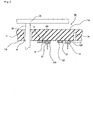
- Fig. 2 is a partially enlarged cross section view of the
ceramic heater illustrated in Fig. 1.
- Fig. 3 is a cross section view which schematically
illustrates the case in which the ceramic heater illustrated
in Fig. 1 is set into a supporting case.
- Fig. 4 is a cross section view which schematically
illustrates one example of the case in which the ceramic heater
of the present invention is used as an electrostatic chuck.
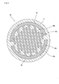
- Fig. 5 is a horizontal cross section view which
schematically illustrates the shape of an electrostatic
electrode constituting the electrostatic chuck according to the
present invention.
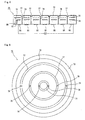
- Fig. 6 is a horizontal cross section view which
schematically illustrates the shape of an electrostatic
electrode constituting the electrostatic chuck according to the
present invention.
- Fig. 7 is a horizontal cross section view which
schematically illustrates the shape of an electrostatic
electrode constituting the electrostatic chuck according to the
present invention.
- Fig. 8 is a cross section view which schematically
illustrates one example of the case in which the ceramic heater
of the present invention is used as a chuck top plate for a wafer
prober.
- Fig. 9 is a plan view which schematically illustrates the
chuck top plate used in the wafer prober of Fig. 8.
- Figs. 10(a) to (d) are cross section views which
schematically illustrate some parts of the manufacturing process
of the ceramic heater illustrated in Fig. 1.
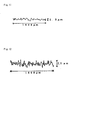
- Fig. 11 is a chart illustrating the surface roughness of
the surface of a resistance heating element formed on a ceramic
heater according to Example 1.
- Fig. 12 is a chart illustrating the surface roughness of
the surface of a resistance heating element formed on a ceramic
heater according to Example 2.
-
Explanation of Numerals
-
- 10
- ceramic heater
- 11, 41, 73
- ceramic substrate
- 11a
- heating face
- 11b
- bottom face
- 12, 45, 85
- resistance heating element
- 120
- metal covering layer
- 13
- external terminal
- 36
- lifter pin
- 39
- semiconductor wafer
- 42, 52, 62
- chuck positive electrostatic layer
- 43, 53, 63
- chuck negative electrostatic layer
- 44
- ceramic dielectric film
- 70
- chuck top plate for a wafer prober
- 72
- chuck top plate
- 75
- guard electrode
- 76
- ground electrode
- 77
- groove
- 86, 87
- conductor-filled through hole
- 90
- supporting case
- 91
- heat-insulating member
- 91a
- substrate-receiving section
- 92
- supporting case body
- 95
- opening
- 97
- metal member for pressing
- 98
- bolt
- 99
- gas-introducing pipe
Detailed Disclosure of the Invention
-
A ceramic heater for a semiconductor-producing/examining
device of the present invention comprises a resistance heating
element on a surface thereof,
wherein
the resistance heating element has a surface roughness
Ra according to JIS B 0601 of 0.01 µm or more.
-
According to the ceramic heater for a
semiconductor-producing/examining device of the present
invention, the surface roughness Ra according to JIS B 0601 of
the surface of the resistance heating element is adjusted to
0.01 µm or more; therefore, the rough face formed on the surface
of resistance heating element functions as heat-radiating fins
when a cooling medium is present around this resistance heating
element so that the resistance heating element is rapidly cooled.
As a result, the temperature of the ceramic heater can be rapidly
lowered.
-
On the other hand, if the surface roughness according to
JIS B 0601 of the surface of the resistance heating element is
less than 0.01 µm, it becomes difficult to lower the temperature
of the ceramic heater rapidly since the heat-radiating effect
of the resistance heating element deteriorates.
-
Fig. 1 is a bottom view which schematically illustrates
a ceramic heater of the present invention, and Fig. 2 is a cross
section view which schematically illustrates one portion of the
ceramic heater illustrated in Fig. 1. Fig. 3 is a cross section
view which schematically illustrates a hot plate unit having
the ceramic heater illustrated in Figs. 1 and 2. In this ceramic
heater, resistance heating elements are formed on the surface
of the ceramic substrate.
-
As illustrated in Fig. 1, a ceramic substrate 11 is formed
in a disc form. In order to perform heating in such a manner
that the temperature of the whole of a heating face 11a of the
ceramic substrate will be uniform, resistance heating elements
12 having a pattern of concentric circle are formed on a bottom
face 11b of the ceramic substrate 11. On the surface thereof,
a metal covering layer 120 is formed.
-
External terminals 13, which will be terminals for input
and output, are connected through the metal covering layer 120
to both ends of each of the resistance heating elements 12. To
the external terminal 13 is fitted, for example, a socket (not
illustrated) having a conductor wire. This conductor wire is
connected to, for example, a power source and so on.
-
At portions near the center of the ceramic substrate 11,
through holes 15, into which lifter pins 36 for carrying a
semiconductor wafer 39 will be inserted, are formed.
Furthermore, bottomed holes 14, into which
temperature-measuring elements (not illustrated) will be
inserted, are formed.
-
A substrate-receiving section 91a for supporting the
ceramic substrate 11 having the resistance heating elements 12
is integrated with the lower inside of a heat-insulating member
91 fitted to the upper portion of a supporting case 90. A
supporting case body 92 having the shape of a bottomed cylinder
is fitted and fixed onto the lower face of the heat-insulating
member 91 with bolts 98.
-
The bolts 98 also have a function of fixing a metal member
97 forpressing. By the metal member 97 for pressing, the ceramic
substrate 11 fitted into the heat-insulating member 91 is pressed
against the substrate-receiving section 91a and fixed.
-
A gas-introducing pipe 99 is fitted to the bottom of the
supporting case body 92, and a heating medium or a cooling medium
is introduced to the inside of the supporting case 90 through
this gas-introducing pipe 99.
-
After the heating medium or the cooling medium, which is
introduced into the supporting case 90, cools or heats the ceramic
substrate 11 and the resistance heating elements 12, the medium
passes through an opening 95 made in the bottom of the supporting
case body 92 and is then discharged outside.
-
The pattern of the resistance heating elements formed in
the ceramic heater of the present invention is not limited to
the concentric pattern illustrated in Fig. 1, and may for example
be a spiral pattern, a pattern comprising repeated circular arcs,
a pattern comprising repeated winding lines, and the like; the
pattern is not particularly limited. These patterns may be
formed alone or in any combination.
-
Resistance heating elements comprising at least two
divided circuits are desirable. By dividing circuits, electric
powers applied to the respective circuits can be controlled so
that the calorific value can be changed and the temperature of
the face for heating the silicon wafer can be adjusted.
-
The thickness of the resistance heating elements is
preferably from 1 to 30 µm, more preferably from 1 to 10 µm.
The width of the resistance heating elements is preferably from
0.1 to 20 mm, more preferably from 0.1 to 5 mm.
-
The resistance values of the resistance heating elements
can be changed depending on their widths and thicknesses.
However, the above-mentioned ranges are most practical.
-
The section shapes of the resistance heating elements may
be rectangular or elliptical, but desirably flat. From the flat
section, heat is more easily radiated toward the heating face.
Thus, a temperature distribution in the heating face is not easily
generated.
-
The aspect ratio (the width of the resistance heating
element/the thickness of the resistance heating element) of the
section is desirably from 10 to 5000.
-
Adjustment thereof into this range makes it possible to
increase the resistance value of the resistance heating elements
and keep the uniformity of the temperature in the heating face.
-
In the case that the thickness of the resistance heating
elements is made to be constant, the amount of heat propagation
to the direction of the heating face of the ceramic substrate
becomes small if the aspect ratio is smaller than the
above-mentioned range. Thus, a thermal distribution similar
to the pattern of the resistance heating elements is generated
in the heating face. On the contrary, if the aspect ratio is
too large, the portions just above the centers of the resistance
heating elements reach a high temperature so that a thermal
distribution similar to the pattern of the resistance heating
elements is generated in the heating face. Accordingly, if
temperature distribution is considered, the aspect ratio of the
section is preferably from 10 to 5000.
-
Regarding a variation in the resistance values of the
resistance heating elements, a variation range of the resistance
values is desirably 5% or less of the average resistance value,
more desirably 1% thereof. The resistance heating elements of
the present invention are plural divided circuits. By making
the variation range of the resistance values as small as described
above, the number of the divided resistance heating elements
can be reduced so that the temperature can easily be controlled.
Furthermore, the temperature of the heating face during the
temperature rise can be made uniform.
-
Usually, such a resistance heating element is formed by:
applying a conductor containing paste comprising metal particles
or conductive ceramic particles for keeping conductivity on a
ceramic substrate and then firing them. The resistance heating
element may also be formed by physical vapor deposition such
as plating or sputtering. In the case of plating, the resistance
heating element can be formed by forming a plating resist. In
the case of sputtering and the like, the resistance heating
element can be formed by performing selective etching.
-
The surface roughness Ra according to the JIS B 0601 of
the resistance heating element is 0.01 µm or more. The surface
roughness is preferably from 0.05 to 15 µm. When the temperature
of the ceramic heater is lowered, a temperature difference
between a cooling medium to be supplied and the resistance heating
element is very large. Therefore, when the surface roughness
Ra is adjusted to 0.01 µm or more, the rough face formed in the
resistance heating element functions as heat-radiating fins.
Thus, the contact area between the cooling medium and the
resistance heating element can be made large and heat exchange
between the cooling medium and the resistance heating element
can be very effectively performed. Consequently, the
temperature of the ceramic substrate can be rapidly lowered.
-
When the rough face is formed in the resistance heating
element, the resistance heating element has a high heat-radiating
effect. Therefore, it is apprehended that when the temperature
thereof is raised, the heating efficiency deteriorates.
However, the ceramic heater of the present invention is usually
held in the supporting case and used as illustrated in Fig. 3,
and when the temperature of the resistance heating element is
raised, gas around the resistance heating element remains in
the supporting case. As a result, the temperature of the gas
around the resistance heating element follows the temperature
of the resistance heating element so that the temperature of
the gas rises. Thus, a temperature difference between the
resistance heating element on a higher temperature side and the
gas around the resistance heating element on a lower temperature
side becomes very small. Therefore, heat exchange between the
two is not performed very much. Consequently, the heating
efficiency of the ceramic heater of the present invention does
not deteriorate very much when the temperature thereof is raised.
-
However, if the surface roughness Ra is 20 µm or more,
the resistance heating element comes to have a very high
heat-radiating effect. For this reason, the resistance heating
element can be rapidly cooled. However, it is apprehended that
the heating efficiency deteriorates.
-
The method of forming a resistance heating element having
such a rough face will be described in detail later. In the
case in which a conductor containing paste is applied to a ceramic
substrate and then sintered, the surface roughness of the
resultant conductor layer can be adjusted by selecting the shape
or the average particle diameter of metal particles, which
constitute a starting material of the resistance heating element.
When a resistance heating element is formed by plating, the
surface roughness can be adjusted by selecting, for example,
conditions for precipitating an acicular crystal and then
performing the plating.
-
The conductor containing paste is not particularly limited,
but is preferably a paste comprising not only the metal particles
or the conductive ceramic but also a resin, a solvent, a thickener
and so on.
-
The above-mentioned metal particles are preferably made
of, for example, a noble metal (gold, silver, platinum or
palladium), lead, tungsten, molybdenum, nickel and the like.
These may be used alone or in combination of two or more kinds
thereof. These metals are not relatively easily oxidized, and
have a resistance value sufficient for generating a heat.
-
Examples of the above-mentioned conductive ceramic
include carbides of tungsten and molybdenum and the like. These
may be used alone or in combination of two or more.
-
The particle diameter of these metal particles or the
conductive ceramic particles is preferably from 0.1 to 100 µm.
If the particle diameter is too small, that is, less than 0.1
µm, the roughness Ra of the surface of the resistance heating
element is liable to be less than 0.01 µm so that the heat-radiating
function of the resistance heating element deteriorates. As
a result, it becomes difficult to lower the temperature of the
ceramic heater rapidly. On the other hand, if the particle
diameter of the metal particles and the like is over 100 µm,
they are not easily sintered so that the resistance value becomes
too large.
-
The shape of the metal particles may be spherical or scaly.
Spherical particles are more preferable, because the surface
of the resistance heating element is easily made coarser. Scaly
particles whose aspect ratio (width or length/thickness) is not
very large are liable to become perpendicular or oblique to the
face on which the resistance heating element is formed; therefore,
the roughness of the surface can be made large.
-
When these metal particles are used, they may be a mixture
of spherical particles and scaly particles.
-
In the case that the metal particles are scaly or a mixture
of spherical particles and scaly particles, metal oxides among
the metal particles are easily held and adhesiveness between
the resistance heating element and a nitride ceramic and the
like is made sure. Moreover, the resistance value can be made
large. Thus, this case is profitable.
-
Furthermore, acicular particles whose aspect ratio
(length to diameter) is not very large are liable to become
perpendicular or oblique to the face on which the resistance
heating element is formed, as well. Therefore, the roughness
of the surface can be made large.
-
Examples of the resin used in the conductor containing
paste include epoxy resins, phenol resins and the like. Examples
of the solvent include isopropyl alcohol and the like. Examples
of the thickener include cellulose and the like.
-
It is desirable to use, as the conductor containing paste,
a paste wherein a metal oxide is added to the metal particles,
and apply this onto the ceramic substrate and subsequently sinter
the metal particles and the like and the metal oxide. This is
because by sintering the metal oxide together with the metal
particles in this way, the nitride ceramic and the like
constituting the ceramic substrate can be closely adhered to
the metal particles.
-
The reason why the adhesiveness to the nitride ceramic
and the like is improved by mixing the metal oxide is unclear,
but would seem to be based on the following. The surface of
the metal particles or the surface of the nitride ceramic and
the like is slightly oxidized so that oxidized films are formed.
The oxidized films are sintered and integrated with each other
through the metal oxide so that the metal particles and the nitride
ceramic and the like are closely adhered to each other. In the
case in which the ceramic constituting the ceramic substrate
is an oxide ceramic, the surface thereof is naturally made of
the oxide. Therefore, a conductor layer having a superior
adhesiveness is formed.
-
A preferred example of the metal oxide is at least one
selected from the group consisting of lead oxide, zinc oxide,
silica, boron oxide (B2O3), alumina, yttria, and titania.
-
These oxides make it possible to improve adhesiveness
between the metal particles and the nitride ceramic and the like
without increasing the resistance value of the resistance heating
elements 12.
-
When the total amount of the metal oxides is set to 100
parts by weight, the weight ratio of above-mentioned lead oxide,
zinc oxide, silica, boron oxide (B2O3), alumina, yttria and
titania is as follows: lead oxide: 1 to 10, silica: 1 to 30,
boron oxide: 5 to 50, zinc oxide: 20 to 70, alumina: 1 to 10,
yttria: 1 to 50 and titania: 1 to 50. This ratio is desirably
adjusted within the scope that the total ratio of the oxides
is not over 100 parts by weight. By adjusting the amounts of
these oxides within these ranges, the adhesiveness to the nitride
ceramic and the like can be particularly improved. The addition
amount of the metal oxides to the metal particles is preferably
0.1% or more by weight and less than 10% by weight.
-
The area resistivity when the conductor containing paste
having such a constitution is used to form the resistance heating
elements 12 is preferably from 1 mΩ/□ to 10 Ω/□ .
-
If the area resistivity is less than 1 mΩ/□ , the resistivity
is too small so that calorific value also becomes small. Thus,
the resistance heating elements do not exhibit their original
function easily. On the other hand, if the area resistivity
is more than 10Ω/□, calorific value for an applied voltage becomes
too large so that in the ceramic heater 10, wherein the resistance
heating elements 12 are formed on the surface of the ceramic
substrate 11, their calorific value is not easily controlled.
-
From the viewpoint of the controllability of the calorific
value, the area resistivity of the resistance heating elements
is more preferably from 1 to 50 mΩ/□ . However, if the area
resistivity is made large, the pattern width (sectional area)
can be made large so that a problem of wire disconnection is
not easily generated. As the case may be, therefore, the area
resistivity is preferably set to 50 mΩ/□ or more.
-
The resistance heating elements are desirably covered with
an insulating covering layer. This is because the oxidation
or sulfurization of the resistance heating elements can be
prevented. As the insulating covering layer, oxide glass, a
resin and the like can be used. Examples of oxide glass include
ZnO-B2O3-SiO2, PbO-SiO2, PbO-B2O3-SiO2, PbO-ZnO-B2O3 and the like.
These oxide glass materials may contain a crystalline portion.
The glass transition point of these glass materials is from 400°C
to 700°C, and the thermal expansion coefficient thereof is from
4 to 9 ppm/°C.
-
Examples of the resin include polyimide resin and silicone
resin and the like. The polyimide resin is a macromolecular
compound obtained by reaction of a carboxylic acid derivative
with a diamine. The silicone resin is a resin wherein a methyl
or ethyl group is arranged as an alkyl group of a side chain
of polysiloxane.
-
The thickness of the insulating covering layer is desirably
from 5 to 100 µm.
-
In the case in which such an insulating covering layer
is formed, the surface roughness Ra of the resistance heating
elements is desirably from 0.05 to 15 µm. This is because the
resistance heating elements are strongly integrated with the
insulating covering layer so that no cracks are generated in
the insulating covering layer by a heat cycle. If the Ra is
less than 0.05 µm, the insulating covering layer moves by the
heat expansion caused by a heat cycle so that a crack is generated.
If the Ra is more than 15 µm, a crack is generated from the tip
of a mountain of the rough face.
-
In the case that the above-mentioned insulating covering
layer is not formed on the resistance heating elements, a metal
covering layer is desirably formed on the surface portion of
the resistance heating elements. This is because a change in
the resistance value, caused by the oxidation of the inner metal
sintered body, is prevented. At this time, the surface roughness
Ra of the metal covering layer to be formed is set to 0.01 µm
or more. The thickness thereof is preferably from 1 to 100 µm.
When the metal covering layer is formed by plating, the surface
roughness can be adjusted by selecting conditions for
precipitating an acicular crystal and then performing the plating.
Furthermore, the surface roughness may be adjusted by forming
a thick plating layer and subsequently performing etching. As
the case may be, it is allowable to form the metal covering layer
on the surface of the resistance heating elements and form the
insulating covering layer thereon. This is because the
resistance heating elements can be more completely protected.
-
Therefore, the surface area of the resistance heating
elements can be made larger, for example, by forming the
resistance heating elements having some degree of surface
roughness by screen printing and the like, and subsequently
forming a plating layer made of an acicular crystal, or by forming
a plating layer having a large thickness and subsequently etching
the layer.
-
The metal used when the metal covering layer is formed
is not particularly limited if the metal is a non-oxidizable
metal. Specifically, examples thereof include gold, silver,
palladium, platinum, nickel and the like. These may be used
alone or in combination of two or more kinds thereof. Among
these, nickel is preferable.
-
The resistance heating element requires a terminal to
connect itself to a power source. This terminal is fixed to
the heating element through solder. Nickel prevents solder from
being thermally diffused. An example of the connecting terminal
is a terminal made of Kovar.
-
The ceramic substrate used in the ceramic heater of the
present invention is desirably in a disc form. The diameter
thereof is desirably more than 200 mm. This is because a
semiconductor wafer having a large diameter can be put onto the
substrate having such a large diameter. It is particularly
desirable that the diameter of the ceramic substrate is 12 inches
(300 mm) or more. Such a ceramic substrate will be suitable
for the mainstream of semiconductor wafers in the next
generation.
-
The thickness of the above-mentioned ceramic substrate
is desirably 25 mm or less. If the thickness of the ceramic
substrate ismore than 25mm, the temperature-following character
deteriorates. The thickness thereof is desirably 0.5 mm or more.
If the thickness is less than 0.5 mm, the strength itself of
the ceramic substrate drops so that the ceramic substrate may
easily be broken down. More desirably, the thickness is above
1.5 mm and 5 mm or less. If the thickness is more than 5 mm,
heat is not easily conducted so that heating efficiency tends
to drop. On the other hand, if the thickness is 1.5 mm or less,
heat conducted in the ceramic substrate does not diffuse
sufficiently so that a variation in temperature may be generated
in the heating face. Moreover, the strength of the ceramic
substrate drops so that the ceramic substrate may be broken down.
-
In the ceramic heater 10 of the present invention, it is
desirable that bottomed holes 14 are made, from the side opposite
to the heating face 11a on which an object to be heated will
be put toward the heating face 11a, in the ceramic substrate
11. Additionally, it is desirable that the bottomof the bottomed
holes 14 is formed nearer to the heating face 11a than the
resistance heating elements 12 and temperature-measuring
elements (not illustrated), such as thermocouples, are set up
into the bottomed holes 14.
-
The distance between the bottoms of the bottomed holes
14 and the heating face 11a is desirably from 0.1 mm to 1/2 of
the thickness of the ceramic substrate.
-
In this way, temperature-measuring positions are nearer
to the heating face 11a than the resistance heating elements
12, so that the temperature of the semiconductor wafer can be
more precisely measured.
-
If the distance between the bottoms of the bottomed holes
14 and the heating face 11a is less than 0.1 mm, heat is radiated
so that temperature distribution is formed in the heating face
11a. If the distance is over 1/2 of the thickness, the ceramic
substrate is easily affected by the temperature of the resistance
heating elements so that temperature-control cannot be performed.
Thus, temperature distribution is formed in the heating face
11a, as well.
-
The diameter of the bottomed holes 14 desirably ranges
from 0.3 mm to 5 mm. If the diameter is too large, heat-radiating
property enhances. If the diameter is too small, workability
deteriorates so that the distance to the heating face 11a cannot
be made uniform.
-
As illustrated in FIG. 1, a plurality of bottomed holes
14 are desirably arranged symmetrically about the center of the
ceramic substrate 11 and arranged into a cross form. This is
because the temperature of the whole of the heating face can
be measured.
-
Examples of the above-mentioned temperature-measuring
element include a thermocouple, a platinum
temperature-measuring resistor, a thermistor and the like.
-
Examples of the above-mentioned thermocouple include K,
R, B, S, E, J and T type thermocouples and the like, as described
in JIS-C-1602 (1980). Among these, the K type thermocouple is
preferable.
-
Desirably, the size of the connecting portions of the
thermocouple is equal to or larger than the strand diameter of
the thermocouple, and is 0.5 mm or less. If the connecting
portion is large, the heat capacity is large so that the response
is slow. It is difficult to make size smaller than the strand
diameter of the thermocouple.
-
The above-mentioned temperature-measuring elements may
be bonded to the bottoms of the bottomed holes 14 with brazing
gold, brazing silver and the like, or may be inserted into the
bottomed holes 14 and then sealed with a heat-resistant resin.
The two may be used together.
-
Examples of the above-mentioned heat-resistant resin
include thermosetting resins, particularly epoxy resin,
polyimide resin, bismaleimide-triazine resin and the like.
These resins may be used alone or in combination of two or more
kinds thereof.
-
As the above-mentioned brazing gold, desirable is at least
one selected from an alloy of 37 to 80.5% by weight of Au and
63 to 19.5% by weight of Cu, and an alloy of 81.5 to 82.5% by
weight of Au and 18.5 to 17.5% by weight of Ni. These have a
melting temperature of 900°C or more, and do not melt easily
in high temperature regions.
-
Examples of the brazing silver that can be used include
Ag-Cu alloys.
-
The ceramic which forms the ceramic heater of the present
invention is desirably a nitride ceramic or a carbide ceramic.
-
The nitride ceramic or the carbide ceramic has a smaller
thermal expansion coefficient than metals and has a far higher
mechanical strength than metals. Therefore, even if the
thickness of the ceramic substrate is made small, the ceramic
substrate is not warped or distorted by heating. For this reason,
the ceramic substrate can be made thin and light. Since the
ceramic substrate has a high thermal conductivity and the ceramic
substrate itself is thin, the surface temperature of the ceramic
substrate follows a change in the temperature of the resistance
heating elements rapidly. That is, by changing a voltage or
electric current value to change the temperature of the
resistance heating elements, the surface temperature of the
ceramic substrate can be controlled.
-
Examples of the above-mentioned nitride ceramic include
aluminum nitride, silicon nitride, boron nitride, titanium
nitride and the like. These maybe used alone or in combination
of two or more kinds thereof.
-
Examples of the carbide ceramic include silicon carbide,
zirconium carbide, titanium carbide, tantalum carbide, tungsten
carbide and the like. These maybe used alone or in combination
of two or more kinds thereof.
-
Among these, aluminum nitride is most preferred. This
is because it has the highest thermal conductivity, that is,
180 W/m · K and it has superior temperature-following character.
-
When a nitride ceramic or a carbide ceramic and the like
is used as the ceramic substrate, an insulating layer may be
formed if necessary. Regarding a nitride ceramic, the volume
resistance value thereof drops easily at high temperature by
solid solution of oxygen and the like. A carbide ceramic has
an electric conductivity unless the ceramic is particularly made
to be of high purity. By forming the insulating layer, a short
between the circuits is prevented at high temperature or even
if it contains impurities. Thus, temperature-controllability
can be ensured.
-
The above-mentioned insulating layer is desirably an oxide
ceramic. Specifically, silica, alumina, mullite, cordierite,
beryllia and the like can be used.
-
Such an insulating layer may be formed by spin-coating
the ceramic substrate with a sol solution wherein an alkoxide
is hydrolyzed and polymerized, and then drying and firing the
solution, or by sputtering, CVD and the like. The surface of
the ceramic substrate may be subjected to oxidation-treatment
to deposit an oxide layer.
-
The above-mentioned insulating layer is desirably from
0.1 to 1000 µm thick. If the thickness thereof is less than
0.1 µm, insulation cannot be ensured. If the thickness is over
1000 µm, heat conductivity from the resistance heating elements
to the ceramic substrate is hindered.
-
Furthermore, the volume resistivity of the
above-mentioned insulating layer is desirably 10 or more times
larger than that of the above-mentioned ceramic substrate (at
the same measurement temperature), because, in the case of less
than 10 times, a short between the circuits cannot be prevented.
-
The ceramic substrate used in the ceramic heater of the
present invention desirably contains carbon. The content
thereof is desirably from 200 to 5000 ppm. This is because the
electrode can be concealed and black-body radiation is easily
used.
-
The brightness of the above-mentioned ceramic substrate
is desirably N6 or less as a value according to the definition
of JIS Z 8721. This is because the ceramic substrate having
a brightness of this degree is superior in heat radiation capacity
and electrode-concealing ability.
-
The brightness N is defined as follows: the brightness
of ideal black is made to 0; that of ideal white is made to 10;
respective colors are divided into 10 parts in the manner that
the brightness of the respective colors is recognized stepwise
between the brightness of black and that of white at equal
intensity intervals; and the resultant parts are indicated by
symbols N0 to N10, respectively.
-
Actual brightness is measured by comparison with color
chips corresponding to N0 to N10. One place of decimals in this
case is made to 0 or 5.
-
In the case in which an electrostatic electrode layer is
formed inside the ceramic substrate in the ceramic heater of
the present invention, the ceramic heater of the present
invention functions as an electrostatic chuck. In this case,
the ceramic substrate constituting this electrostatic chuck is
made in substantially the same way as the above-mentioned ceramic
heater except that an electrostatic electrode is formed.
-
Fig. 4 is a vertical cross section view schematically
illustrating an embodiment of an electrostatic chuck according
to the present invention, and Fig. 5 is a cross section view
taken on A-A line of the electrostatic chuck illustrated in Fig.
4.
-
In this electrostatic chuck 40, an electrostatic electrode
layer comprising a chuck positive electrostatic layer 42 and
a chuck negative electrostatic layer 43 is embedded in a ceramic
substrate 41. A thin ceramic layer 44 (hereinafter referred
to as a ceramic dielectric layer) is formed on this electrostatic
electrode layer. A silicon wafer 39 is put on the electrostatic
chuck 40 and grounded.
-
As illustrated in FIG. 5, the chuck positive electrostatic
layer 42 comprises a semicircular arc part 42a and a comb teeth
shaped part 42b. Likewise, the chuck negative electrostatic
layer 43 comprises a semicircular arc part 43a and a comb teeth
shaped part 43b. The chuck positive electrostatic layer 42 and
chuck negative electrostatic layer 43 are arranged face-to-face
in such a manner that the teeth of one comb teeth shaped part
42b extend in staggered relation with the teeth of the other
comb teeth shaped part 43b. The + side and the - side of a direct
current power source are connected to the chuck positive
electrostatic layer 42 and chuck negative electrostatic layer
43, respectively, so that a direct current voltage V2 is applied
thereto.
-
In order to control the temperature of the semiconductor
wafer 39, resistance heating elements 45 in the formof concentric
circles as viewed from the above, as illustrated in FIG. 1, are
formed on the ceramic substrate 41. Regarding the surface of
the resistance heating elements 45, its surface roughness Ra
according to JIS B 0601 is adjusted to 0.01 µm or more. External
terminals are connected and fixed to both ends of each of the
resistance heating elements 45, and a voltage V1 is applied
thereto. Although not illustrated in Figs. 4 and 5, bottomed
holes, into which temperature-measuring elements will be
inserted, and through holes, through which lifter pins that
support the silicon wafer 39 and move it up and down are inserted,
are formed in the ceramic substrate 41.
-
When this electrostatic chuck 40 is caused to work, a direct
current voltage V2 is applied to the chuck positive electrostatic
layer 42 and the chuck negative electrostatic layer 43. In this
way, the semiconductor wafer 39 is adsorbed and fixed onto the
chuck positive electrode and the chuck negative electrode through
the ceramic dielectric film 44 by electrostatic effect of the
chuck positive electrostatic layer 42 and the chuck negative
electrostatic layer 43. The semiconductor wafer 39 is fixed
onto the electrostatic chuck 40 in this way, and subsequently
the semiconductor wafer 39 is subjected to various treatments
such as CVD.
-
In the electrostatic chuck according to the present
invention, the rough face formed on the surface of the resistance
heating elements functions as heat-radiating fins in the same
way as in the above-mentioned ceramic heater when a cooling medium
is present around the resistance heating elements. Thus, the
electrostatic chuck is rapidly cooled. As a result, the
temperature of the electrostatic chuck can be rapidly lowered.
-
Examples of the above-mentioned electrostatic electrodes
include a sintered body of a metal or a conductive ceramic; a
metal foil; and the like. As the metal sintered body, at least
one selected from tungsten and molybdenum is preferred. The
metal foil is desirably made of the same material for the metal
sintered body. These metals are relatively not easily oxidized
and have a sufficient conductivity for electrodes. As the
conductive ceramic, at least one selected from carbides of
tungsten and molybdenum can be used.
-
Figs. 6 and 7 are horizontal cross section views, each
of which schematically illustrates electrostatic electrodes in
a different electrostatic chuck. In an electrostatic chuck 50
illustrated in FIG. 6, a chuck positive electrostatic layer 52
and a chuck negative electrostatic layer 53 in a semicircular
form are formed inside a ceramic substrate 41. In an
electrostatic chuck 60 illustrated in FIG. 7, chuck positive
electrostatic layers 62a and 62b and chuck negative electrostatic
layers 63a and 63b, each of which is quartered-circle shaped,
are formed inside a ceramic substrate 41. The two chuck positive
electrostatic layers 62a and 62b and the two chuck negative
electrostatic layers 63a and 63b are formed to cross each other.
-
When the electrodes are formed in segments of a circle,
for instance, the number of segments is not particularly limited
and may be 5 or more. The shape thereof is not limited to a
sector.
-
In a ceramic heater of the present invention, by depositing
a chuck top conductor layer on the surface of the ceramic substrate
and disposing guard electrodes and ground electrodes and the
like inside of the ceramic substrate, the resultant ceramic
heater of the present invention functions as a chuck top plate
for a wafer prober.
-
FIG. 8 is a cross section view which schematically
illustrates a chuck top plate for a wafer prober according to
the present invention. FIG. 9 is a plan view which schematically
illustrates the chuck top plate for a wafer prober illustrated
in FIG. 8.
-
In the chuck top plate for a wafer prober (hereinafter
referred to also as the wafer prober) 70, grooves 77 in the form
of concentric circles are formed on the surface of a disc-form
ceramic substrate 73. Moreover, plural suction holes 78 for
sucking a silicon wafer are made in some parts of the grooves
7. A chuck top conductor layer 72 for connecting electrodes
of the semiconductor wafer is formed, in a circular form, in
the greater part of the ceramic substrate 73 including the grooves
77. A semiconductor wafer is put on this chuck top conductor
layer and a probe card having a tester pin is pressed against
it, whereby a continuity test is performed.
-
In order to control the temperature of the silicon wafer,
resistance heating elements 85 as illustrated in Fig. 1, in the
form of concentric circles as viewed from the above, are made
on the bottom face of the ceramic substrate 73. Regarding the
surface of the resistance heating elements 85, their surface
roughness Ra according to JIS B 0601 is adjusted to 0.01 µm or
more. External terminals (not illustrated) are connected and
fixed to both ends of the resistance heating elements 85. Guard
electrodes 75 for canceling stray capacitor lying in the
measuring-circuit are formed in the ceramic substrate 73, and
a ground voltage of the measuring-circuit (that is, the chuck
top conductor layer 72) is given thereto. Ground electrodes
76 are formed to cancel noises from temperature-controlling
means.
-
In the wafer prober according to the present invention,
the rough faces formed on a surface of the resistance heating
elements function as heat-radiating fins in the same way as in
the above-mentioned ceramic heater when a cooling medium is
present around the resistance heating elements. Thus, the wafer
prober is rapidly cooled. As a result, the temperature of the
wafer prober can be rapidly lowered.
-
The thickness of the chuck top conductor layer 72 is
desirably from 1 to 20 µm. As the chuck top conductor layer,
there can be used, for example, at least one metal selected from
high melting point metals such as copper, titanium, chromium,
nickel, noblemetals (gold, silver, platinum and so on), tungsten,
molybdenum and the like.
-
A noble metal layer (not illustrated) is formed on the
chuck top conductor layer 72, and the noble metal layer prevents
diffusion of boron or phosphorous in the chuck top conductor
layer, or yttria, sodium and the like in the ceramic without
hindering electrical conduction to the back face of the
semiconductor wafer. As the noble metal, at least one selected
from gold, silver, platinum and palladium is desirable.
-
The following will describe a process for producing a
ceramic heater of the present invention according to Fig. 10.
- (1) Manufacturing process of a ceramic substrate
A sintering aid such as yttria (Y2O3), a compound containing
Na or Ca, a binder and so on are blended as appropriate with
powder of a ceramic such as aluminum nitride, to prepare a slurry.
Thereafter, this slurry is made into a granular form by
spray-drying and the like. The granule is put into a mold and
pressed to be formed into a plate form and the like. Thus, a
raw formed body (green) is formed.The raw formed body may also be formed by laminating green
sheets formed by a doctor blade method and the like.Next, the following portions are made in the raw formed
body if necessary: portions that will be through holes 15 into
which lifter pins 36 for carrying an object to be heated and
the like, such as a silicon wafer 39, will be inserted; portions
that will be bottomed holes 14 in which temperature-measuring
elements such as thermocouples will be buried; and so on.Next, this raw formed body is heated and fired to be sintered.
Thus, a plate made of the ceramic is manufactured. Thereafter,
the plate is made into a given shape to produce a ceramic substrate
11 (see Fig. 10(a)). The shape of the raw formed body may be
such a shape that the sintered body can be used as it is.
Additionally, for example, by heating and firing the raw formed
body under pressure from the upper and lower sides, the ceramic
substrate 11 having no pores can be manufactured. It is
sufficient that the heating and the firing are performed at
sintering temperature or higher. For example, for nitride
ceramics, the firing temperature is from 1000°C to 2500°C.After the firing, the through holes 15 and the bottomed
holes 14 in which the temperature-measuring elements will be
inserted are usually made. The through holes 15 and so on can
be formed by conducting blast treatment, such as sandblast using
SiC particles and the like, after grinding the surface.
- (2) Process of printing a conductor containing paste on the
ceramic substrate
A conductor containing paste is generally a highly viscous
fluid comprising metal particles, a resin and a solvent. The
viscosity of this conductor containing paste is preferably from
70 to 90 Pa•s. If the viscosity of the conductor containing
paste is less than 70 Pa•s, the viscosity is too low to prepare
a paste containing the metals and so on which have a uniform
concentration. As a result, a conductor layer having a uniform
thickness is not easily formed. On the other hand, if the
viscosity is more than 90 Pa•s, the viscosity of the conductor
containing paste is too high so that coating work becomes
difficult. Thus, a conductor layer having a uniform thickness
is not easily formed, either. In order to form a conductor layer
having a rough face, the conductor containing paste preferably
has a higher viscosity. This is because it is easy for the metals
in a scaly or an acicular form to be perpendicular or oblique
to the face of resistance heating elements.This conductor containing paste is subjected to
screen-printing and the like, to form a conductor containing
paste layer, which will be a pattern of resistance heating
elements 12. The method of forming the resistance heating
elements may be the method of using the conductor containing
" paste, or a method of forming a plating layer by plating and
then firing the layer, thereby forming the resistance heating
elements. In this case, the resistance heating elements having
rough faces can be formed by precipitating plating to form an
acicular plating layer . In this case, it is desirable that after
a thin film is formed by electroless plating and the like, an
acicular plating layer is formed on this thin film by
electroplating and the like. It is also allowable to form a
thick plating layer and subject the layer to etching and the
like, thereby forming a rough face.The surface roughness of the resistance heating elements
is most greatly affected by the average particle diameter of
the metal particles. Therefore, the surface roughness of the
resistance heating elements is usually controlled by controlling
the average particle diameter of the metal particles.
Furthermore, the surface roughness may be adjusted by buff
grinding, sandblast treatment and the like.
- (3) Firing of the conductor containing paste
The conductor containing paste layer printed on the bottom
face of the ceramic substrate 11 is heated or fired to remove
the resin and the solvent and further sinter the metal particles.
Thus, the metal particles are baked onto the bottom face of the
ceramic substrate 11 to form the resistance heating elements
(see Fig. 10(b)). In this case, the roughness of the surface of the resistance
heating elements can be adjusted by changing heating and firing
conditions. The heating and firing temperature is usually from
500°C to 1000°C. By firing the paste layer at a relatively low
temperature, it is possible to prevent the metal and so on from
melting and the surface from being flat. Thus, the surface
roughness Ra of the conductor layer can be set to 0.01 µm or
more. However, if the heating and firing temperature is too
low, sintering between the metals does not advance so that the
resistance value of the resistance heating elements becomes too
high. Therefore, it is necessary to select an appropriate firing
temperature depending on the metal to be used.
- (4) Forming of a metal covering layer
A metal covering layer 120 is desirably deposited on the
surface of the resistance heating elements 12, as illustrated
in Fig. 2 (see Fig. 10 (c) ) . The metal covering layer 120 can
be formed by electroplating, electroless plating, sputtering
and the like. From the viewpoint of mass-productivity,
electroless plating is optimal. Instead of the formation of
the metal covering layer, the above-mentioned insulating
covering layer may be formed. It is also allowable to form the
metal covering layer 120 on the surface of the resistance heating
elements 12 and subsequently form the insulating covering layer
thereon.
- (5) Fitting of terminals and so on
Terminals (external terminals 13) for connection to a power
source are fitted up to ends of the pattern of the resistance
heating elements 12 with solder (see Fig. 10(d)). Thermocouples
are inserted into the bottomed holes 14. The bottomed holes
are sealed with a heat resistant resin such as polyimide to finish
the manufacture of a ceramic heater.
-
-
A process for manufacturing an electrostatic chuck
according to the present invention will be described.
- (1) Process of producing green sheets
First, powder of a ceramic such as nitride ceramic is mixed
with a binder, a solvent and so on to prepare a paste. This
is used to produce green sheets.As the above-mentioned ceramic powder such as nitride
ceramic, aluminum nitride and the like can be used. If necessary,
a sintering aid such as yttria or a compound containing Na or
Ca may be added.As the binder, desirable is at least one selected from
an acrylic binder, ethylcellulose, butylcellosolve, and
polyvinyl alcohol.As the solvent, desirable is at least one selected from
α-terpineol and glycol.A paste obtained by mixing these is molded into a sheet
form by a doctor blade method, to produce a green sheet.The thickness of the green sheet is preferably 0.1 to 5
mm.
- (2) Process of printing a conductor containing paste on the green
sheet
A conductor containing paste which contains a metal paste
or a conductive ceramic, for forming a chuck positive
electrostatic layer and a chuck negative electrostatic layer,
is printed on the green sheet to form a conductor containing
paste layer. Conductor containing paste-filled layer, which
will form a conductor-filled through hole, is formed in the
through holes.These conductor containing pastes contain the metal
particles or the conductive ceramic particles.The average particle diameter of tungsten particles or
molybdenum particles is preferably from 0.1 to 5 µm. If the
average particle diameter is less than 0.1 µm or more than 5
µm, the conductor containing paste is not easily printed.Such a conductor containing paste may be a composition
(paste) obtained by mixing, for example, 85 to 87 parts by weight
of the metal particles or the conductive ceramic particles; 1.5
to 10 parts by weight of at least one binder selected from acrylic
binders, ethylcellulose, butylcellosolve and polyvinyl
alcohol; and 1.5 to 10 parts by weight of at least one solvent
selected from α-terpineol and glycol.
- (3) Process of manufacturing a ceramic substrate
-
-
Green sheets on which no conductor containing paste is
printed are laminated on the upper and lower sides of the green
sheet on which the conductor containing paste is printed.
Thereafter, by thermal pressure-bonding, a green sheet
lamination is formed. The green sheet lamination is heated and
pressed so as to sinter the green sheets and the inner conductor
containing paste.
-
The heating temperature is preferably from 1000°C to 2000°C,
and the pressing pressure is preferably from 10 to 20 MPa. The
heating is performed in the atmosphere of an inert gas. As the
inert gas, argon, nitrogen and the like can be used.
-
Thereafter, the sintered body is subjected to surface
grinding followed by blast treatment such as sandblast using
SiC particles, thereby making through holes and bottomed holes
in which temperature-measuring elements will be inserted. In
this way, a ceramic substrate having, inside it, a chuck positive
electrostatic layer and a chuck negative electrostatic layer
is completed.
-
The resultant ceramic substrate is subjected to the same
processes (2) to (5) as in the manufacturing method of the
above-mentioned ceramic heater, thereby manufacturing an
electrostatic chuck according to the present invention.
-
By embedding metal foil in the raw formed body in the shapes
of the chuck positive electrostatic layer and the chuck negative
electrostatic layer in the process (1) of the manufacturing
method of the above-mentioned ceramic heater, an electrostatic
chuck according to the present invention can be manufactured
in the same way as the manufacturing method of the above-mentioned
ceramic heater.
-
As a method for manufacturing a wafer prober according
to the present invention, the same method for manufacturing the
ceramic heater can be used except the following: in the
manufacturing method of the above-mentioned electrostatic chuck,
the same method of forming the chuck positive electrostatic layer
and the chuck negative electrostatic layer inside the ceramic
substrate is used to form guard electrodes and ground electrodes;
blast treatment such as sandblast using SiC particles is
conducted to form grooves and through holes; and subsequently
sputtering and the like is used to form a chuck top conductor
layer.
Best Mode for Carrying Out the Invention
-
Hereinafter, the present invention will be described in
more detail by means of Examples.
(Example 1) Manufacture of a ceramic heater (see Figs. 1 and
2)
-
- (1) A composition made of 100 parts by weight of aluminum
nitride powder (average particle diameter: 0.6 µm), 4 parts by
weight of yttria (average particle diameter: 0.4 µm), 12 parts
by weight of an acrylic binder, and an alcohol was subjected
to spray-drying to produce granular powder.
- (2) Next, this granular powder was put into a mold and
molded into a flat plate form, to obtain a raw formed body (green) .
- (3) Next, this raw formed body was hot-pressed at 1800°C
and a pressure of 20 MPa to yield an aluminum nitride plate having
a thickness of about 3 mm.
Next, a disc having a diameter of 210 mm was cut out from
this plate to prepare a plate made of the ceramic (ceramic
substrate 11). This ceramic substrate was drilled to form
through holes 15, into which lifter pins 36 for a silicon wafer
would be inserted, and bottomed holes 14 (diameter: 1.1 mm, and
depth: 2 mm), in which thermocouples would be buried.
- (4) A conductor containing paste layer was formed on the
ceramic substrate 11 obtained in the above-mentioned (3) by
screen printing. The printed pattern was a pattern as
illustrated in Fig. 1.
The above-mentioned conductor containing paste was a paste
having a composition of Ag: 48% by weight, Pt: 21% by weight,
SiO2: 1.0% by weight, B2O3: 1.2% by weight, ZnO: 4.1% by weight,
PbO: 3.4% by weight, ethyl acetate: 3.4% by weight, and butyl
carbitol: 17.9% by weight.This conductor containing paste was aAg-Pt paste. Silver
particles (Ag-540 made by Shoei Chemical Inc.) thereof had an
average particle diameter of 4.5 µm, and were scaly. Pt particles
(Pt-221 made by Shoei Chemical Inc.) thereof had an average
particle diameter of 6.8 µm, and were spherical.The viscosity of the conductor containing paste at this
time was 80 Pa•s.
- (5) Furthermore, the ceramic substrate 11 was heated and
fired at 850°C for 20 minutes after the formation of the conductor
containing paste layer for a heating element pattern, so as to
sinter Ag and Pt in the conductor containing paste and bake Ag
and Pt onto the substrate 11. In this way, resistance heating
elements 12 were formed.
- (6) Next, portions to which external terminals 13 for
ensuring connection to a power source would be fitted were
subjected to Ni plating, and subsequently a silver-lead solder
paste (made by Tanaka Kikinzoku Co.) was printed by screen
printing, so as to form a solder layer.
Next, the external terminals 13 made of Kovar were put
on the solder layer, and heated and reflowed at 420°C to fit
the external terminals 13 to the surface of the resistance heating
elements 12.
- (7) Thermocouples for controlling temperature were
sealed with polyimide, to yield a ceramic heater 10.
-
(Example 2) Manufacture of a ceramic heater
-
A ceramic heater was manufactured in the same way as in
Example 1 except that as the conductor containing paste, a paste
having the following composition was used and then heating and
firing were performed to form resistance heating elements.
-
As the above-mentioned conductor containing paste, the
following was used: a silver paste containing 7.5 parts by weight
of metal oxides, relative to 100 parts by weight of silver,
containing lead oxide: 5% by weight, zinc oxide: 55% by weight,
silica: 10% by weight, boron oxide: 25% by weight and alumina:
5% by weight. Silver particles (Ag-540 made by Shoei Chemical
Inc.) thereof had an average particle diameter of 4.5 µm, and
were scaly.
-
The viscosity of the conductor containing paste at this
time was 80 Pa•s.
-
Furthermore, after the formation of the conductor
containingpaste layer for a heating element pattern, the ceramic
substrate was heated and fired at 780°C for 20 minutes, so as
to sinter silver and lead in the conductor containing paste and
bake them onto the ceramic substrate.
(Example 3) Manufacture of a ceramic heater
-
A ceramic heater was manufactured in the same way as in
Example 1 except that after the heating and firing the conductor
containing paste to form resistance heating elements, the
resistance heating elements were subjected to sandblast
treatment using alumina having an average particle diameter of
10 µm.
(Example 4)
-
A ceramic heater was manufactured in the same way as in
Example 1 except that Solvest PS603 made by Tokuriki Chemical
Research Co., Ltd. was used as the conductor containing paste
and fired at 780°C for 10 minutes to form resistance heating
elements, and the resistance heating elements were subjected
to sandblast treatment using alumina particles having an average
particle diameter of 0.1 µm.
(Example 5) Manufacture of a ceramic heater
-
A ceramic heater was manufactured in the same way as in
Example 1 except that after the heating and firing the conductor
containing paste to form resistance heating elements, the
resistance heating elements were subjected to sandblast
treatment using silicon carbide particles having an average
particle diameter of 10 µm.
(Example 6) Manufacture of a ceramic heater
-
A ceramic heater was manufactured in the same way as in
Example 1 except that after the heating and firing the conductor
containing paste to form resistance heating elements, the
resistance heating elements were subjected to sandblast
treatment using silicon carbide particles having an average
particle diameter of 20 µm.
(Example 7) Manufacture of a ceramic heater
-
A ceramic heater was manufactured in the same way as in
Example 1 except that after the heating and firing the conductor
containing paste to form resistance heating elements, the
resistance heating elements were subjected to sandblast
treatment using silicon carbide particles having an average
particle diameter of 30 µm.
(Examples 8 to 13)
-
A glass paste (G-5270 made by Shoei Chemical Inc.) was
applied to the surface of each of the ceramic heaters manufactured
in Examples 1 to 6, and subsequently the ceramic heater was fired
at 600°C to form a glass coat on the surface.
(Comparative Example 1) Manufacture of a ceramic heater
-
A ceramic heater was manufactured in the same way as in
Example 1 except that the following paste was used as the conductor
containing paste and the paste was heated and fired to form
resistance heating elements.
-
The above-mentioned conductor containing paste was
Solvest PS603 made by Tokuriki Chemical Research Co., Ltd. The
viscosity of the conductor containing paste at this time was
80 Pa•s.
-
Furthermore, after the formation of the conductor
containing paste layer for a heating element pattern, the ceramic
substrate was heated and fired at 780°C for 10 minutes, so as
to sinter silver in the conductor containing paste andbake silver
onto the ceramic substrate.
-
Each of the ceramic substrates according to Examples 1
to 7 and Comparative Example 1 was put on a supporting case
illustrated in Fig. 3. Thereafter, a semiconductor wafer was
put thereon and an electric current was sent thereto so as to
raise the temperature to 300°C. Next, the supply of the electric
power was stopped and a cooling medium was supplied thereto so
as to drop the temperature to 250°C. The ceramic substrate was
evaluated by the following methods (1) and (2). As the cooling
medium, air at a room temperature (20°C) was supplied at 0.1
m3/minute from a gas-introducing pipe fitted to the supporting
case.
-
The ceramic heaters according to Examples 8 to 13 were
evaluated by the following method (3).
-
The results are shown in Tables 1 and 2.
Evaluation method
-
- (1) Measurement of the surface roughness Ra of the
conductor layer (resistance heating elements)
A surface roughness meter (Surfcom 920A, made by Tokyo
Seimitsu Co.) was used to measure the surface roughness Ra of
the surface of the resistance heating elements on the ceramic
substrate formed in each of Examples and Comparative Example
by a method according to JIS B 0601. The surface roughness Ra
obtained from the measurement results are shown in Table 1. The
surface roughness Ra obtained from the measurement results of
Examples 1 and 2 are shown in Table 1. Charts showing the
measurement results of Examples 1 and 2 are shown in Figs. 11
and 12, respectively.
- (2) Measurement of temperature rising time and
temperature dropping time
The following were measured: temperature rising time when
the temperature was raised from room temperature to 300°C and
temperature dropping time when the temperature was lowered from
300°C to 250°C.The results are shown in Table 1.
- (3) Heat cycle test
About each of the six ceramic heaters according to Examples
8 to 13, a heat cycle test within the range of 25°C to 500°C
was repeatedly carried out 500 times to check whether a crack
was generated or not. The results are shown in Table 2.
| | Surface roughness Ra of the resistance heating elements (µm) | Temperature rising speed (second) | Temperature dropping speed (second) |
| Example 1 | 0.30 | 45 | 150 |
| Example 2 | 0.86 | 46 | 150 |
| Example 3 | 9.8 | 45 | 130 |
| Example 4 | 0.04 | 45 | 150 |
| Example 5 | 15.1 | 46 | 120 |
| Example 6 | 20.0 | 48 | 120 |
| Example 7 | 28.5 | 60 | 100 |
| Comparative Example 1 | 0.008 | 45 | 180 |
| | Surface roughness Ra of the resistance heating elements (µm) | Crack |
| Example 8 | 0.30 | Not generated |
| Example 9 | 0.86 | Not generated |
| Example 10 | 9.8 | Not generated |
| Example 11 | 0.04 | Generated |
| Example 12 | 15.1 | Not generated |
| Example 13 | 20.0 | Generated |
-
-
As is evident from the results shown in Table 1, the ceramic
heater according to Example 7, which had a surface roughness
Ra of 28.5 µm, had the shortest temperature dropping time of
100 seconds. The ceramic heaters according to Examples 1 to
7 had a shorter temperature dropping time than the ceramic heater
according to Comparative Example. This would be based on the
following reason. Since in the ceramic heaters according to
Examples the surface roughness Ra of the surface of their
resistance heating elements was adjusted to 0.01 µm or more,
the rough face formed on the surface of the resistance heating
elements functioned as heat-radiating fins when the cooling
medium was present around the resistance heating elements. Thus,
the resistance heating elements were rapidly cooled so that the
temperature of the ceramic substrates was able to drop rapidly.
-
The ceramic heaters according to Examples 6 and 7, which
had a surface roughness Ra of 20 µm or more, had a long temperature
rising time since they had a high heat-radiating effect.
-
On the other hand, the ceramic heater according to
Comparative Example 1, which had a surface roughness Ra of 0.008
µm, had the temperature dropping time of 180 seconds. That is,
it required a far longer time for temperature dropping than the
ceramic heaters according to Examples. This would be based on
the following reason. Since in the ceramic heater according
to Comparative Example the surface roughness Ra of the surface
of its resistance heating elements was less than 0.01 µm, the
heat-radiating effect of the resistance heating elements
deteriorated. As a result, rapid temperature dropping of the
ceramic substrate was difficult.
-
A little difference in the temperature rising time, which
appears to be caused by the difference in the surface roughness,
was generated between the ceramic heaters according to Examples
and Comparative Example. However, this difference is evidently
smaller than the difference in the temperature dropping time.
This wouldbe based on the following reason. When the temperature
dropped, a temperature difference was very large between the
supplied cooling medium and the resistance heating elements.
Therefore, a great deal of heat was exchanged between the cooling
medium and the resistance heating elements. On the other hand,
when the temperature was raised, the temperature of the gas,
which stayed inside the supporting case surrounding the
resistance heating elements, followed the temperature of the
resistance heating elements so that the temperature of the gas
rose. As a result, a temperature difference became small between
the resistance heating elements on a higher temperature side
and the gas surrounding the resistance heating elements on a
lower temperature side, so that heat was not exchanged very much
between the two.
Industrial Applicability
-
As described above, according to the ceramic heater of
the present invention, the surface roughness Ra according to
JIS B 0601 of resistance heating elements formed on the surface
of the heater is 0.01 µm or more. Therefore, when a cooling
medium was present around the heater, the rough face formed on
the surface of the resistance heating elements functioned as
heat-radiating fins. Thus, the resistance heating elements
were rapidly cooled, and the temperature of the ceramic heater
was able to drop rapidly.