EP1340991A2 - System and method for testing a circuit - Google Patents
System and method for testing a circuit Download PDFInfo
- Publication number
- EP1340991A2 EP1340991A2 EP03004683A EP03004683A EP1340991A2 EP 1340991 A2 EP1340991 A2 EP 1340991A2 EP 03004683 A EP03004683 A EP 03004683A EP 03004683 A EP03004683 A EP 03004683A EP 1340991 A2 EP1340991 A2 EP 1340991A2
- Authority
- EP
- European Patent Office
- Prior art keywords
- scan
- output
- input
- flop
- sequential
- Prior art date
- Legal status (The legal status is an assumption and is not a legal conclusion. Google has not performed a legal analysis and makes no representation as to the accuracy of the status listed.)
- Granted
Links
Images




Classifications
-
- G—PHYSICS
- G01—MEASURING; TESTING
- G01R—MEASURING ELECTRIC VARIABLES; MEASURING MAGNETIC VARIABLES
- G01R31/00—Arrangements for testing electric properties; Arrangements for locating electric faults; Arrangements for electrical testing characterised by what is being tested not provided for elsewhere
- G01R31/28—Testing of electronic circuits, e.g. by signal tracer
- G01R31/317—Testing of digital circuits
- G01R31/3181—Functional testing
- G01R31/3185—Reconfiguring for testing, e.g. LSSD, partitioning
- G01R31/318533—Reconfiguring for testing, e.g. LSSD, partitioning using scanning techniques, e.g. LSSD, Boundary Scan, JTAG
- G01R31/318594—Timing aspects
-
- G—PHYSICS
- G01—MEASURING; TESTING
- G01R—MEASURING ELECTRIC VARIABLES; MEASURING MAGNETIC VARIABLES
- G01R31/00—Arrangements for testing electric properties; Arrangements for locating electric faults; Arrangements for electrical testing characterised by what is being tested not provided for elsewhere
- G01R31/28—Testing of electronic circuits, e.g. by signal tracer
- G01R31/317—Testing of digital circuits
- G01R31/3181—Functional testing
- G01R31/3185—Reconfiguring for testing, e.g. LSSD, partitioning
- G01R31/318533—Reconfiguring for testing, e.g. LSSD, partitioning using scanning techniques, e.g. LSSD, Boundary Scan, JTAG
- G01R31/318541—Scan latches or cell details
Definitions
- a conventional scan chain provides a system and a method for testing for defects in, for example, sequential devices and combinational logic circuits of the VLSIC.
- the sequential devices e.g., flip flops or flops
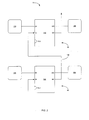
- the VLSIC includes sequential devices 10, 20 and combinational logic circuits 30.
- the conventional scan chain system consists of many flops, however only two of the flops are shown for illustration.
- a first flop 10 and a second flop 20 have inputs and outputs.
- each flop 10, 20 has a data input DI, a scan input SI, a clock input CLK and a data output DO.
- the data input DI is connected to combinational logic circuit 30 of the VLSIC.
- the clock input CLK is connected to a clock of the VLSIC (not shown).
- the data output DO is connected to the combinational logic circuit 30.
- the present invention may provide a system for testing a circuit.
- the system may include, for example, a first flop and a second flop.
- Each of the first flop and the second flop may include a scan input, a delay buffer, a scan output and a data output.
- the data output may be coupled to the scan input and to the scan output.
- the data output may be coupled to the scan output via the delay buffer.
- the scan output of the first flop is coupled directly to the scan input of the second flop via an interconnect.
- a sequential device may include, for example, any type of flip flop (i.e., flop) or sets of flops or other types of sequential devices.
- the VLSIC may include, for example, sequential devices 80, 90 and combinational logic circuits 30.
- the sequential devices 80, 90 include flops 100, 110, respectively.
- the scan chain 70 may include one or more flops, however, only two of the flops 100, 110 are illustrated in FIG. 2.
- a first flop 100 and a second flop 110 may include inputs and outputs. Some of the inputs and outputs of a flop known to one of ordinary skill in the art may not be shown here.
- an input test vector is scanned through the serial chain of flops.
- the input test vector is a known set of values (e.g., binary zeroes and ones).
- the length of the input test vector is related (e.g., equal) to the length of the serial chain of flops.
- the input test vector is scanned in serially one bit at a time through the serial chain.
- each of the flops processes the input signal from the scan input SI instead of from the data input DI.
- the input signal from the scan input SI or the data input DI may subsequently be carried by the scan output SO and the data output DO, the scan output SO possibly carrying the signal after a time delay.
- the scan path in the example shown in FIG. 2 passes through the scan input SI of the first flop 100, the scan output SO of the first flop 100, the wire 130, the scan input SI of the second flop 110, the scan output SO of the second flop and so on.
- the data input signals to the flops are loaded in parallel via the data inputs DI of the flops.
- the data input signals to the flops may be a function of at least one of the combinational logic circuit 120 and the data outputs DO of the flops.
- the output signals on the scan outputs SO can then be scanned out via an enabling signal received by the scan enabling inputs SI which may cause the flops to go into a scan mode or a shift mode as described above.
- the output signals on the scan outputs SO which are shifted out of the VLSIC, may form a set of values (e.g., a string of binary zeroes and ones) which is known as an output test vector.
- an output test vector can be generated for each input test vector scanned into the scan chain 70.
- the output test vector can then be compared with the expected test vector to see whether or not a defect exists in the VLSIC.
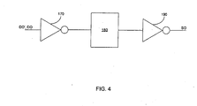
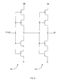
- the first CMOS transistor arrangement 230 may be structured to invert its input signal and to provide isolation between the data outputs DO', DO and the scan output SO.
- the first CMOS arrangement 230 may be structured to provide a high intrinsic delay (even without much loading). In one example, the intrinsic delay is high enough to ensure that, even with a light load, any time violations (e.g., a hold time violation) are prevented.
- the CMOS transistors 210, 220, 240, 250 may be structured to provide delay by providing poor drive strength. For example, poor drive strength may be achieved by making the width of the CMOS transistors 210, 220, 240, 250 short and the length of the CMOS transistors 210, 220, 240, 250 long.
- the overall area taken up by the flop 140 including the delay buffer 160 may be equal to or less than the overall area taken up by the conventional flop 10, 20 and the buffer 40 as illustrated in FIG. 1.
Landscapes
- Engineering & Computer Science (AREA)
- General Engineering & Computer Science (AREA)
- Physics & Mathematics (AREA)
- General Physics & Mathematics (AREA)
- Tests Of Electronic Circuits (AREA)
- Semiconductor Integrated Circuits (AREA)
Abstract
Description
The
Claims (25)
- A sequential device for use in a scan chain, comprising:a scan input;a scan output; anda functional data output coupled to the scan input and to the scan output, the functional data output being coupled to the scan output via a delay buffer.
- The sequential device according to claim 1, wherein the scan output and the functional data output are separate outputs.
- The sequential device according to claim 1, wherein the delay buffer is structured to isolate the scan output from the functional data output.
- The sequential device according to claim 1, wherein the delay buffer is structured to provide a time delay.
- The sequential device according to claim 1, wherein the delay buffer comprises an inverter and a transmission gate.
- The sequential device according to claim 5, where in the inverter is structured to isolate the scan output from the functional data output.
- The sequential device according to claim 5, wherein the transmission gate provides a time delay.
- The sequential device according to claim 1, wherein the delay buffer comprises an inverter and a complementary metal oxide semiconductor (CMOS) transistor arrangement.
- The sequential device according to claim 8, wherein the inverter is structured to provide isolation between the scan output and the function data output.
- The sequential device according to claim 8, wherein the CMOS transistor arrangement is structured to have at least one of weak drive strength and high intrinsic delay.
- The sequential device according to claim 1, wherein the delay buffer comprises a first CMOS transistor arrangement and a second CMOS transistor arrangement.
- The sequential device according to claim 11, wherein at least one of the first CMOS transistor arrangement and the second CMOS transistor arrangement comprises at least two p-channel MOS (PMOS) transistors and at least two n-channel MOS (NMOS) transistors in a totem pole configuration.
- The sequential device according to claim 11, wherein at least one of the first CMOS transistor arrangement and the second CMOS transistor arrangement comprises MOS transistors with small widths and long lengths so as to have poor drive strength.
- The sequential device according to claim 1, wherein the scan input, the delay buffer and the scan output are part of a scan chain path.
- The sequential device according to claim 1, wherein the delay buffer is structured to prevent a timing violation in the sequential device.
- The sequential device according to claim 15, wherein the timing violation comprises a hold time violation.
- A system for testing a circuit, comprising:a first flop comprising a first scan input, a first delay buffer, a first scan output, a first data output, the first data output being coupled to the first scan input and to the first scan output, the first data output being coupled to the first scan output via the first delay buffer; anda second flop comprising a second scan input, a second delay buffer, a second scan output, a second data output, the second data output being coupled to the second scan input and to the second scan output, the second data output being coupled to the second scan output via the second delay buffer, the second scan input being coupled directly to the first scan output via an interconnect.
- The system according to claim 17, wherein a scan chain comprises the first flop and the second flop.
- The system according to claim 18, wherein the scan chain comprises a scan path comprising the first scan input, the first delay buffer, the first scan output, the second scan input, the second delay buffer and the second scan output.
- The system according to claim 17, wherein the interconnect is a single wire.
- The system according to claim 17, wherein the first delay buffer and the second delay buffer provide isolation circuitry and a time delay, the time delay being adapted to avoid timing violations in the first flop and the second flop.
- A method for testing a circuit using a scan chain, comprising the steps of:connecting sequential devices in a serial chain, each of the sequential devices having a dedicated scan output that is isolated from a functional data output;shifting an input test vector into the serial chain via the dedicated scan outputs of the sequential devices;loading functional data inputs of the sequential devices;carrying the loaded functional data inputs on the functional data outputs and the dedicated scan outputs of the sequential devices; andshifting an output test vector out of the serial chain via the dedicated scan outputs of the sequential devices.
- The method according to claim 22, wherein the step of connecting comprises connecting the dedicated scan output of a first sequential device to a dedicated scan input of a second device with a single interconnect.
- The method according to claim 22, wherein the step of loading comprises loading, in parallel, the data inputs of the sequential devices.
- The method according to claim 22, wherein the step of carrying comprises carrying the loaded functional data inputs on the dedicated scan outputs of the sequential devices after a delay.
Applications Claiming Priority (4)
| Application Number | Priority Date | Filing Date | Title |
|---|---|---|---|
| US187116 | 1980-09-15 | ||
| US36100402P | 2002-03-01 | 2002-03-01 | |
| US361004P | 2002-03-01 | ||
| US10/187,116 US6968488B2 (en) | 2002-03-01 | 2002-06-28 | System and method for testing a circuit |
Publications (3)
| Publication Number | Publication Date |
|---|---|
| EP1340991A2 true EP1340991A2 (en) | 2003-09-03 |
| EP1340991A3 EP1340991A3 (en) | 2004-09-15 |
| EP1340991B1 EP1340991B1 (en) | 2008-04-02 |
Family
ID=27737031
Family Applications (1)
| Application Number | Title | Priority Date | Filing Date |
|---|---|---|---|
| EP03004683A Expired - Lifetime EP1340991B1 (en) | 2002-03-01 | 2003-03-03 | System and method for testing a circuit |
Country Status (3)
| Country | Link |
|---|---|
| US (2) | US6968488B2 (en) |
| EP (1) | EP1340991B1 (en) |
| DE (1) | DE60320057T2 (en) |
Cited By (1)
| Publication number | Priority date | Publication date | Assignee | Title |
|---|---|---|---|---|
| WO2016069203A1 (en) * | 2014-10-30 | 2016-05-06 | Qualcomm Incorporated | Scan path for test mode with signal delay elements by delay circuits having different supply voltages |
Families Citing this family (5)
| Publication number | Priority date | Publication date | Assignee | Title |
|---|---|---|---|---|
| US6968488B2 (en) * | 2002-03-01 | 2005-11-22 | Broadcom Corporation | System and method for testing a circuit |
| US7240260B2 (en) * | 2002-12-11 | 2007-07-03 | Intel Corporation | Stimulus generation |
| US9432020B2 (en) | 2014-06-25 | 2016-08-30 | Stmicroelectronics S.R.L. | Communication cell for an integrated circuit operating in contact and contactless mode, electronic chip comprising the communication cell, electronic system including the chip, and test apparatus |
| KR20220142212A (en) * | 2021-04-14 | 2022-10-21 | 삼성전자주식회사 | Multi-bit flip-flop and integrated circuit including the same |
| CN116562206A (en) * | 2022-01-27 | 2023-08-08 | 瑞昱半导体股份有限公司 | Calibration data generating circuit and related method |
Family Cites Families (21)
| Publication number | Priority date | Publication date | Assignee | Title |
|---|---|---|---|---|
| JPH03252569A (en) | 1990-02-26 | 1991-11-11 | Advanced Micro Devicds Inc | Register circuit for scan pass |
| JP2811872B2 (en) | 1990-02-26 | 1998-10-15 | 富士電機株式会社 | Semiconductor device protection circuit |
| US5329167A (en) * | 1992-09-25 | 1994-07-12 | Hughes Aircraft Company | Test flip-flop with an auxillary latch enabling two (2) bits of storage |
| JP3229164B2 (en) * | 1994-07-28 | 2001-11-12 | インターナショナル・ビジネス・マシーンズ・コーポレーション | Latch circuit |
| JP3363691B2 (en) * | 1996-03-13 | 2003-01-08 | シャープ株式会社 | Semiconductor logic integrated circuit |
| US5642364A (en) * | 1996-06-28 | 1997-06-24 | Hughes Electronics | Contactless testing of inputs and outputs of integrated circuits |
| US5907562A (en) | 1996-07-31 | 1999-05-25 | Nokia Mobile Phones Limited | Testable integrated circuit with reduced power dissipation |
| US5886901A (en) | 1997-01-07 | 1999-03-23 | Lsi Logic Corporation | Flip-flop for scan test chain |
| US5896046A (en) * | 1997-01-27 | 1999-04-20 | International Business Machines Corporation | Latch structure for ripple domino logic |
| US5887004A (en) * | 1997-03-28 | 1999-03-23 | International Business Machines Corporation | Isolated scan paths |
| US6708303B1 (en) * | 1998-03-06 | 2004-03-16 | Texas Instruments Incorporated | Method and apparatus for controlling a seperate scan output of a scan circuit |
| US6389566B1 (en) * | 1998-06-02 | 2002-05-14 | S3 Incorporated | Edge-triggered scan flip-flop and one-pass scan synthesis methodology |
| US6272654B1 (en) * | 1999-03-04 | 2001-08-07 | International Business Machines Corporation | Fast scannable output latch with domino logic input |
| KR20010102343A (en) * | 1999-12-24 | 2001-11-15 | 롤페스 요하네스 게라투스 알베르투스 | Low power scan flipflop |
| US6377098B1 (en) * | 2000-04-21 | 2002-04-23 | International Business Machines Corporation | CMOS latch having a selectable feedback path |
| US6775116B2 (en) * | 2001-11-01 | 2004-08-10 | Agilent Technologies, Inc. | Method and apparatus for preventing buffers from being damaged by electrical charges collected on lines connected to the buffers |
| US7039843B2 (en) * | 2001-11-13 | 2006-05-02 | Sun Microsystems, Inc. | Modeling custom scan flops in level sensitive scan design |
| US6968488B2 (en) * | 2002-03-01 | 2005-11-22 | Broadcom Corporation | System and method for testing a circuit |
| US6925590B2 (en) * | 2002-04-22 | 2005-08-02 | Broadcom Corporation | Scan interface |
| US6904554B2 (en) * | 2002-06-26 | 2005-06-07 | Lsi Logic Corporation | Logic built-in self test (BIST) |
| JP2004301661A (en) * | 2003-03-31 | 2004-10-28 | Hitachi Ltd | Semiconductor integrated circuit |
-
2002
- 2002-06-28 US US10/187,116 patent/US6968488B2/en not_active Expired - Fee Related
-
2003
- 2003-03-03 EP EP03004683A patent/EP1340991B1/en not_active Expired - Lifetime
- 2003-03-03 DE DE60320057T patent/DE60320057T2/en not_active Expired - Lifetime
-
2005
- 2005-05-19 US US11/132,673 patent/US7836365B2/en not_active Expired - Fee Related
Cited By (2)
| Publication number | Priority date | Publication date | Assignee | Title |
|---|---|---|---|---|
| WO2016069203A1 (en) * | 2014-10-30 | 2016-05-06 | Qualcomm Incorporated | Scan path for test mode with signal delay elements by delay circuits having different supply voltages |
| US9678154B2 (en) | 2014-10-30 | 2017-06-13 | Qualcomm Incorporated | Circuit techniques for efficient scan hold path design |
Also Published As
| Publication number | Publication date |
|---|---|
| US7836365B2 (en) | 2010-11-16 |
| EP1340991A3 (en) | 2004-09-15 |
| US6968488B2 (en) | 2005-11-22 |
| EP1340991B1 (en) | 2008-04-02 |
| DE60320057D1 (en) | 2008-05-15 |
| US20050216807A1 (en) | 2005-09-29 |
| US20030167430A1 (en) | 2003-09-04 |
| DE60320057T2 (en) | 2009-05-20 |
Similar Documents
| Publication | Publication Date | Title |
|---|---|---|
| KR0131185B1 (en) | Logic circuit | |
| US6861866B2 (en) | System on chip (SOC) and method of testing and/or debugging the system on chip | |
| KR100335683B1 (en) | Method and apparatus for utilizing mux scan flip-flops to test speed related defects | |
| JP3802377B2 (en) | Flip-flop and scan path circuit | |
| US5450418A (en) | Pseudo master slave capture mechanism for scan elements | |
| US4942577A (en) | Logic circuit system with latch circuits for reliable scan-path testing | |
| US5426650A (en) | Full scan optimization technique using drive one/drive zero elements and multiple capture clocking | |
| US6529033B1 (en) | Area efficient clock inverting circuit for design for testability | |
| US6968488B2 (en) | System and method for testing a circuit | |
| JP4108374B2 (en) | Scan flip-flop circuit, scan flip-flop circuit array, and integrated circuit device | |
| US6487688B1 (en) | Method for testing circuits with tri-state drivers and circuit for use therewith | |
| EP1179740A2 (en) | Boundary scan chain routing | |
| JP3363691B2 (en) | Semiconductor logic integrated circuit | |
| US7230446B2 (en) | Semiconductor logic circuit device having pull-up/pull-down circuit for input buffer pad and wafer-probing testing method therefor | |
| US6496030B1 (en) | Scan flip-flop providing both scan and propagation delay testing | |
| KR20020064630A (en) | Integrated circuit device having boundary scan register | |
| EP1324208A1 (en) | Circuit device for transmitting bus signals | |
| US7032146B2 (en) | Boundary scan apparatus and interconnect test method | |
| US6020772A (en) | Flash output LSSD latch | |
| US20060242505A1 (en) | Apparatus for performing stuck fault testings within an integrated circuit | |
| US7644331B2 (en) | System and method for testing and debugging analog circuits in a memory controller | |
| JPH07119790B2 (en) | Semiconductor integrated device | |
| US7463063B2 (en) | Semiconductor device | |
| JPH05160682A (en) | flip flop | |
| US20030115555A1 (en) | A method and apparatus for integrating boundary-scan multiplexer functionality within a pad driver |
Legal Events
| Date | Code | Title | Description |
|---|---|---|---|
| PUAI | Public reference made under article 153(3) epc to a published international application that has entered the european phase |
Free format text: ORIGINAL CODE: 0009012 |
|
| AK | Designated contracting states |
Kind code of ref document: A2 Designated state(s): AT BE BG CH CY CZ DE DK EE ES FI FR GB GR HU IE IT LI LU MC NL PT SE SI SK TR |
|
| AX | Request for extension of the european patent |
Extension state: AL LT LV MK RO |
|
| PUAL | Search report despatched |
Free format text: ORIGINAL CODE: 0009013 |
|
| AK | Designated contracting states |
Kind code of ref document: A3 Designated state(s): AT BE BG CH CY CZ DE DK EE ES FI FR GB GR HU IE IT LI LU MC NL PT SE SI SK TR |
|
| AX | Request for extension of the european patent |
Extension state: AL LT LV MK RO |
|
| 17P | Request for examination filed |
Effective date: 20050315 |
|
| 17Q | First examination report despatched |
Effective date: 20050412 |
|
| AKX | Designation fees paid |
Designated state(s): DE FR GB |
|
| 17Q | First examination report despatched |
Effective date: 20050412 |
|
| RAP1 | Party data changed (applicant data changed or rights of an application transferred) |
Owner name: BROADCOM CORPORATION |
|
| GRAP | Despatch of communication of intention to grant a patent |
Free format text: ORIGINAL CODE: EPIDOSNIGR1 |
|
| GRAS | Grant fee paid |
Free format text: ORIGINAL CODE: EPIDOSNIGR3 |
|
| GRAA | (expected) grant |
Free format text: ORIGINAL CODE: 0009210 |
|
| AK | Designated contracting states |
Kind code of ref document: B1 Designated state(s): DE FR GB |
|
| REG | Reference to a national code |
Ref country code: GB Ref legal event code: FG4D |
|
| REF | Corresponds to: |
Ref document number: 60320057 Country of ref document: DE Date of ref document: 20080515 Kind code of ref document: P |
|
| ET | Fr: translation filed | ||
| PLBE | No opposition filed within time limit |
Free format text: ORIGINAL CODE: 0009261 |
|
| STAA | Information on the status of an ep patent application or granted ep patent |
Free format text: STATUS: NO OPPOSITION FILED WITHIN TIME LIMIT |
|
| 26N | No opposition filed |
Effective date: 20090106 |
|
| PGFP | Annual fee paid to national office [announced via postgrant information from national office to epo] |
Ref country code: FR Payment date: 20130329 Year of fee payment: 11 Ref country code: GB Payment date: 20130318 Year of fee payment: 11 |
|
| GBPC | Gb: european patent ceased through non-payment of renewal fee |
Effective date: 20140303 |
|
| REG | Reference to a national code |
Ref country code: FR Ref legal event code: ST Effective date: 20141128 |
|
| PG25 | Lapsed in a contracting state [announced via postgrant information from national office to epo] |
Ref country code: GB Free format text: LAPSE BECAUSE OF NON-PAYMENT OF DUE FEES Effective date: 20140303 Ref country code: FR Free format text: LAPSE BECAUSE OF NON-PAYMENT OF DUE FEES Effective date: 20140331 |
|
| PGFP | Annual fee paid to national office [announced via postgrant information from national office to epo] |
Ref country code: DE Payment date: 20160331 Year of fee payment: 14 |
|
| REG | Reference to a national code |
Ref country code: DE Ref legal event code: R082 Ref document number: 60320057 Country of ref document: DE Representative=s name: BOSCH JEHLE PATENTANWALTSGESELLSCHAFT MBH, DE Ref country code: DE Ref legal event code: R081 Ref document number: 60320057 Country of ref document: DE Owner name: AVAGO TECHNOLOGIES GENERAL IP (SINGAPORE) PTE., SG Free format text: FORMER OWNER: BROADCOM CORP., IRVINE, CALIF., US |
|
| REG | Reference to a national code |
Ref country code: DE Ref legal event code: R119 Ref document number: 60320057 Country of ref document: DE |
|
| PG25 | Lapsed in a contracting state [announced via postgrant information from national office to epo] |
Ref country code: DE Free format text: LAPSE BECAUSE OF NON-PAYMENT OF DUE FEES Effective date: 20171003 |