EP1340737B1 - Semiconductive polycrystalline diamond - Google Patents
Semiconductive polycrystalline diamond Download PDFInfo
- Publication number
- EP1340737B1 EP1340737B1 EP03251153A EP03251153A EP1340737B1 EP 1340737 B1 EP1340737 B1 EP 1340737B1 EP 03251153 A EP03251153 A EP 03251153A EP 03251153 A EP03251153 A EP 03251153A EP 1340737 B1 EP1340737 B1 EP 1340737B1
- Authority
- EP
- European Patent Office
- Prior art keywords
- diamond
- pcd
- semiconductive
- layer
- crystals
- Prior art date
- Legal status (The legal status is an assumption and is not a legal conclusion. Google has not performed a legal analysis and makes no representation as to the accuracy of the status listed.)
- Expired - Fee Related
Links
Images


Classifications
-
- B—PERFORMING OPERATIONS; TRANSPORTING
- B22—CASTING; POWDER METALLURGY
- B22F—WORKING METALLIC POWDER; MANUFACTURE OF ARTICLES FROM METALLIC POWDER; MAKING METALLIC POWDER; APPARATUS OR DEVICES SPECIALLY ADAPTED FOR METALLIC POWDER
- B22F7/00—Manufacture of composite layers, workpieces, or articles, comprising metallic powder, by sintering the powder, with or without compacting wherein at least one part is obtained by sintering or compression
- B22F7/06—Manufacture of composite layers, workpieces, or articles, comprising metallic powder, by sintering the powder, with or without compacting wherein at least one part is obtained by sintering or compression of composite workpieces or articles from parts, e.g. to form tipped tools
-
- C—CHEMISTRY; METALLURGY
- C04—CEMENTS; CONCRETE; ARTIFICIAL STONE; CERAMICS; REFRACTORIES
- C04B—LIME, MAGNESIA; SLAG; CEMENTS; COMPOSITIONS THEREOF, e.g. MORTARS, CONCRETE OR LIKE BUILDING MATERIALS; ARTIFICIAL STONE; CERAMICS; REFRACTORIES; TREATMENT OF NATURAL STONE
- C04B35/00—Shaped ceramic products characterised by their composition; Ceramics compositions; Processing powders of inorganic compounds preparatory to the manufacturing of ceramic products
- C04B35/515—Shaped ceramic products characterised by their composition; Ceramics compositions; Processing powders of inorganic compounds preparatory to the manufacturing of ceramic products based on non-oxide ceramics
- C04B35/52—Shaped ceramic products characterised by their composition; Ceramics compositions; Processing powders of inorganic compounds preparatory to the manufacturing of ceramic products based on non-oxide ceramics based on carbon, e.g. graphite
-
- C—CHEMISTRY; METALLURGY
- C23—COATING METALLIC MATERIAL; COATING MATERIAL WITH METALLIC MATERIAL; CHEMICAL SURFACE TREATMENT; DIFFUSION TREATMENT OF METALLIC MATERIAL; COATING BY VACUUM EVAPORATION, BY SPUTTERING, BY ION IMPLANTATION OR BY CHEMICAL VAPOUR DEPOSITION, IN GENERAL; INHIBITING CORROSION OF METALLIC MATERIAL OR INCRUSTATION IN GENERAL
- C23C—COATING METALLIC MATERIAL; COATING MATERIAL WITH METALLIC MATERIAL; SURFACE TREATMENT OF METALLIC MATERIAL BY DIFFUSION INTO THE SURFACE, BY CHEMICAL CONVERSION OR SUBSTITUTION; COATING BY VACUUM EVAPORATION, BY SPUTTERING, BY ION IMPLANTATION OR BY CHEMICAL VAPOUR DEPOSITION, IN GENERAL
- C23C24/00—Coating starting from inorganic powder
- C23C24/08—Coating starting from inorganic powder by application of heat or pressure and heat
-
- C—CHEMISTRY; METALLURGY
- C23—COATING METALLIC MATERIAL; COATING MATERIAL WITH METALLIC MATERIAL; CHEMICAL SURFACE TREATMENT; DIFFUSION TREATMENT OF METALLIC MATERIAL; COATING BY VACUUM EVAPORATION, BY SPUTTERING, BY ION IMPLANTATION OR BY CHEMICAL VAPOUR DEPOSITION, IN GENERAL; INHIBITING CORROSION OF METALLIC MATERIAL OR INCRUSTATION IN GENERAL
- C23C—COATING METALLIC MATERIAL; COATING MATERIAL WITH METALLIC MATERIAL; SURFACE TREATMENT OF METALLIC MATERIAL BY DIFFUSION INTO THE SURFACE, BY CHEMICAL CONVERSION OR SUBSTITUTION; COATING BY VACUUM EVAPORATION, BY SPUTTERING, BY ION IMPLANTATION OR BY CHEMICAL VAPOUR DEPOSITION, IN GENERAL
- C23C30/00—Coating with metallic material characterised only by the composition of the metallic material, i.e. not characterised by the coating process
- C23C30/005—Coating with metallic material characterised only by the composition of the metallic material, i.e. not characterised by the coating process on hard metal substrates
-
- B—PERFORMING OPERATIONS; TRANSPORTING
- B22—CASTING; POWDER METALLURGY
- B22F—WORKING METALLIC POWDER; MANUFACTURE OF ARTICLES FROM METALLIC POWDER; MAKING METALLIC POWDER; APPARATUS OR DEVICES SPECIALLY ADAPTED FOR METALLIC POWDER
- B22F5/00—Manufacture of workpieces or articles from metallic powder characterised by the special shape of the product
- B22F2005/001—Cutting tools, earth boring or grinding tool other than table ware
-
- C—CHEMISTRY; METALLURGY
- C04—CEMENTS; CONCRETE; ARTIFICIAL STONE; CERAMICS; REFRACTORIES
- C04B—LIME, MAGNESIA; SLAG; CEMENTS; COMPOSITIONS THEREOF, e.g. MORTARS, CONCRETE OR LIKE BUILDING MATERIALS; ARTIFICIAL STONE; CERAMICS; REFRACTORIES; TREATMENT OF NATURAL STONE
- C04B2235/00—Aspects relating to ceramic starting mixtures or sintered ceramic products
- C04B2235/02—Composition of constituents of the starting material or of secondary phases of the final product
- C04B2235/30—Constituents and secondary phases not being of a fibrous nature
- C04B2235/40—Metallic constituents or additives not added as binding phase
- C04B2235/402—Aluminium
-
- C—CHEMISTRY; METALLURGY
- C04—CEMENTS; CONCRETE; ARTIFICIAL STONE; CERAMICS; REFRACTORIES
- C04B—LIME, MAGNESIA; SLAG; CEMENTS; COMPOSITIONS THEREOF, e.g. MORTARS, CONCRETE OR LIKE BUILDING MATERIALS; ARTIFICIAL STONE; CERAMICS; REFRACTORIES; TREATMENT OF NATURAL STONE
- C04B2235/00—Aspects relating to ceramic starting mixtures or sintered ceramic products
- C04B2235/02—Composition of constituents of the starting material or of secondary phases of the final product
- C04B2235/30—Constituents and secondary phases not being of a fibrous nature
- C04B2235/40—Metallic constituents or additives not added as binding phase
- C04B2235/404—Refractory metals
-
- C—CHEMISTRY; METALLURGY
- C04—CEMENTS; CONCRETE; ARTIFICIAL STONE; CERAMICS; REFRACTORIES
- C04B—LIME, MAGNESIA; SLAG; CEMENTS; COMPOSITIONS THEREOF, e.g. MORTARS, CONCRETE OR LIKE BUILDING MATERIALS; ARTIFICIAL STONE; CERAMICS; REFRACTORIES; TREATMENT OF NATURAL STONE
- C04B2235/00—Aspects relating to ceramic starting mixtures or sintered ceramic products
- C04B2235/02—Composition of constituents of the starting material or of secondary phases of the final product
- C04B2235/30—Constituents and secondary phases not being of a fibrous nature
- C04B2235/40—Metallic constituents or additives not added as binding phase
- C04B2235/405—Iron group metals
-
- C—CHEMISTRY; METALLURGY
- C04—CEMENTS; CONCRETE; ARTIFICIAL STONE; CERAMICS; REFRACTORIES
- C04B—LIME, MAGNESIA; SLAG; CEMENTS; COMPOSITIONS THEREOF, e.g. MORTARS, CONCRETE OR LIKE BUILDING MATERIALS; ARTIFICIAL STONE; CERAMICS; REFRACTORIES; TREATMENT OF NATURAL STONE
- C04B2235/00—Aspects relating to ceramic starting mixtures or sintered ceramic products
- C04B2235/02—Composition of constituents of the starting material or of secondary phases of the final product
- C04B2235/30—Constituents and secondary phases not being of a fibrous nature
- C04B2235/42—Non metallic elements added as constituents or additives, e.g. sulfur, phosphor, selenium or tellurium
- C04B2235/421—Boron
-
- C—CHEMISTRY; METALLURGY
- C04—CEMENTS; CONCRETE; ARTIFICIAL STONE; CERAMICS; REFRACTORIES
- C04B—LIME, MAGNESIA; SLAG; CEMENTS; COMPOSITIONS THEREOF, e.g. MORTARS, CONCRETE OR LIKE BUILDING MATERIALS; ARTIFICIAL STONE; CERAMICS; REFRACTORIES; TREATMENT OF NATURAL STONE
- C04B2235/00—Aspects relating to ceramic starting mixtures or sintered ceramic products
- C04B2235/02—Composition of constituents of the starting material or of secondary phases of the final product
- C04B2235/30—Constituents and secondary phases not being of a fibrous nature
- C04B2235/42—Non metallic elements added as constituents or additives, e.g. sulfur, phosphor, selenium or tellurium
- C04B2235/422—Carbon
- C04B2235/427—Diamond
-
- C—CHEMISTRY; METALLURGY
- C04—CEMENTS; CONCRETE; ARTIFICIAL STONE; CERAMICS; REFRACTORIES
- C04B—LIME, MAGNESIA; SLAG; CEMENTS; COMPOSITIONS THEREOF, e.g. MORTARS, CONCRETE OR LIKE BUILDING MATERIALS; ARTIFICIAL STONE; CERAMICS; REFRACTORIES; TREATMENT OF NATURAL STONE
- C04B2235/00—Aspects relating to ceramic starting mixtures or sintered ceramic products
- C04B2235/70—Aspects relating to sintered or melt-casted ceramic products
- C04B2235/96—Properties of ceramic products, e.g. mechanical properties such as strength, toughness, wear resistance
Definitions
- This invention relates to polycrystalline diamond and more specifically to semiconductive polycrystalline diamond that exhibits enhanced cuttability, especially Electro-Discharge Machining or Electro-Discharge Grinding cuttability.
- PCD Polycrystalline diamond
- HTHP high temperature/high pressure
- Such PCD materials are ultra hard materials well known for their mechanical property of high wear resistance, making them a popular material choice for use in such industrial applications as cutting tools for machining, and subterranean mining and drilling, where the mechanical property of wear resistance is highly desired.
- conventional PCD materials can be provided in the form of a surface coating, e.g., on inserts used with cutting and drilling tools, to improve wear resistance of the insert.
- PCD inserts used in such applications are produced by forming one or more layers of PCD-based material over a suitable substrate material.
- Such inserts also referred to as cutting elements, comprise a substrate, a PCD surface layer, and optionally one or more transition layers to improve the bonding between the exposed PCD surface layer and the underlying substrate support layer.
- Substrates used in such insert applications are commonly formed from a carbide material such as tungsten carbide, WC, cemented with cobalt, Co, and commonly referred to as a cemented tungsten carbide, WC/Co system.
- the layer or layers of PCD conventionally may include a metal binder therein.
- the metal binder is used to facilitate intercrystalline bonding between diamond grains, and acts to bond the layers to each other and to the underlying substrate.
- the metal binder material is generally included at a weight percentage of about 10% by weight.
- Metals conventionally employed as the binder are often selected from the group including cobalt, iron, or nickel and/or mixtures or alloys thereof.
- the binder material may also include metals such as manganese, tantalum, chromium and/or mixtures or alloys thereof.
- the metal binder may be provided in powder form as an ingredient for forming the PCD material, or can be drawn into the PCD material from the substrate material during HTHP processing also referred to as the "sintering" process.
- the amount of binder material that is used to form PCD materials represents a compromise between the desired material properties of toughness and hardness/wear resistance. While a higher metal binder content typically increases the toughness of the resulting PCD material, higher metal content also decreases the PCD material hardness, wear resistance and thermal stability. Thus, these inversely affected desired properties ultimately limit the flexibility of being able to provide PCD coatings having desired levels of both wear resistance and toughness to meet the service demands of particular applications. Additionally, when the PCD composition is chosen to increase the wear resistance of the PCD material, typically brittleness also increases, thereby reducing the toughness of the PCD material.
- the PCD After the PCD is formed, it must be cut to desired shapes for use in a cutting tool. Cutting is typically accomplished using Electro-Discharge Machining (EDM) or Electro-Discharge Grinding (EDG) operations which are well known in the art.
- EDM Electro-Discharge Machining
- EDG Electro-Discharge Grinding
- the metal binder in the PCD forms a metallic matrix and provides conductivity that supports EDM or EDG cutting.
- cooling fluid or dielectric fluid used for cooling during EDM or EDG cutting may leach out the metal matrix from the PCD and significantly increase the resistance of the PCD layer.
- PCD material that has enhanced EDM and EDG cuttability without a reduction in material hardness, wear resistance and thermal stability.
- the present invention is directed to a polycrystalline diamond (PCD) ultra hard material and a method for forming the same.
- the polycrystalline diamond ultra hard material includes semiconductive diamond crystals therein.
- the semiconductive diamond crystals may be diamond crystals doped with lithium, beryllium or aluminum.
- the polycrystalline diamond ultra hard material is formed of conventional diamond crystals, at least some of which include semiconductive outer surface layers. According to either of the aforementioned exemplary embodiments, the polycrystalline diamond ultra hard material is a semiconductor material.
- a method for forming a cutting element comprising:
- a semiconductive polycrystalline diamond material formed by sintering comprising diamond crystals doped with a material selected from the group consisting of Be, Li and Al.
- a cutting element is formed by providing a substrate and forming a polycrystalline diamond layer over the substrate.
- the polycrystalline diamond layer is formed over the substrate by providing a layer of diamond powder comprising non-conductive diamond grit feedstock and an additive, and converting the layer of diamond powder to polycrystalline diamond that is a solid semiconductor material.
- the additive may be chosen from the group consisting of lithium, beryllium, boron, and aluminum.
- Diamond grit feedstock composed of conventional, insulative diamond crystals, for example Type I diamond crystals, may be used.
- a cutting element is formed by providing a layer of diamond grit feedstock including diamond crystals doped with at least one of beryllium, lithium and aluminum, then sintering to convert the layer of diamond grit feedstock to a semiconductive, solid polycrystalline diamond layer.
- the ultra hard PCD layer is formed as a semiconductor material with increased conductivity compared to PCD layers formed of conventional insulative diamond crystals, such as Type I diamond crystals. Even if all the metal binder materials that may be included in the PCD layer are removed by leaching, the cuttability of the semiconductive PCD material of the present invention is enhanced, especially EDM and EDG cuttability.
- a PCD material having enhanced cuttability, especially EDM and EDG cuttability without comprising its hardness, wear resistance, or thermal stability, cutting and other tools incorporating such material, and a method of making such material and tools, are provided.
- An exemplary embodiment PCD material of the present invention has a substantial percentage of diamond crystals that are semiconductive in nature or which include semiconductive outer surface layers. Such diamond crystals contain small quantities of interstitial impurities such as lithium (Li), beryllium (Be), boron (B), and aluminum (Al) that are sufficient to make them semiconductors.
- PCD formed with conventional diamond crystals that are electrical insulators includes a much higher resistance than the PCD of the present invention. This is true both for PCD materials which include metal binder materials therein, and PCD materials void of such metal binder materials.
- An exemplary embodiment PCD of the present invention is formed by using semiconductive diamond grit feedstock formed of semiconductive diamond crystals doped with Li, Be or Al or combinations thereof.
- PCD may be formed by using a combination of semiconductive and conventional, non-conductive diamond grit feedstock such as Type I diamond grit feedstock.
- the PCD is formed using conventional undoped diamond grit feedstock (such as Type I diamond grit feedstock) together with a suitable quantity of additives such as B, Li, Be and Al. The additives diffuse throughout the diamond lattice so as to cause the diamond crystals to transform to diamond crystals that include semiconductive surface layers.
- the PCD material formed according to each of the aforementioned methods is semiconductive in nature.
- both the PCD material formed using semiconductive diamond grit feedstock and the PCD material formed using conventional diamond grit feedstock and an additive to convert the diamond crystals to having semiconductive surface layers will be collectively referred to as semiconductive PCD.
- the semiconductive PCD of the present invention is a solid structural body commonly referred to as an ultra-hard material or ultra-hard layer and may be used as a cutting layer on cutting tools and cutting elements, or a wear resistant layer for other applications.
- cutting elements and cutting tools are referred to as "cutting elements" hereinafter.
- the semiconductive PCD may be a layer formed over a substrate to produce a cutting element.
- the cutting element may be inserted into a drill bit and used for earth boring.
- the semiconductive PCD of the present invention may be used in various other applications and industries, in other exemplary embodiments.
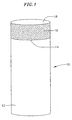
- FIG. 1 shows cutting element 10 formed of substrate 12 and ultra hard layer 16 which is also referred to as a cutting table and includes top surface 18.
- Ultra hard layer 16 is formed of semiconductive PCD in the present invention.
- Interface 14 is formed between substrate 12 and ultra hard layer 16.
- one or more transition layers may be formed between ultra hard layer 16 and substrate 12.
- the generally cylindrically-shaped cutting element illustrated in FIG. 1 is intended to be exemplary only and according to various other exemplary embodiments, the cutting elements and ultra-hard layers may take on any of various other shapes.
- the cutting element is mounted on a bit such as the drag bit shown in FIG. 2, and contacts the earthen formation along edge 28, during drilling.
- the cutting elements 10 are joined to pockets or other receiving shapes that extend into drag bit body 24 by brazing or other means well known in the art.
- the illustrated arrangement is intended to be exemplary only and cutting elements 10 may be used in various other arrangements in other exemplary embodiments.
- the method for forming the semiconductive PCD material includes providing a substrate and providing a layer of diamond powderoverthe substrate, then using HTHP processing to sinter, thereby solidifying the layer of diamond powder and converting the same to an ultra-hard layer of PCD, and also bonding the PCD layer to the substrate to form a cutting element.
- the substrate may be a pre-formed solid substrate, or it may be provided in powder form and also solidified during the sintering operation.
- the substrate may be formed of various matrix materials.
- the substrate may be formed of cemented tungsten carbide.
- Cemented tungsten carbide generally refers to tungsten carbide particles disbursed in a substrate binder metal matrix such as iron, nickel, or cobalt.
- substrate materials may be used in other exemplary embodiments.
- Wear resistant materials suitable for use as the substrate may be selected from compounds of carbide and metals selected from Groups IVB, VB, VIB, and VIIB of the Periodic Table of the Elements. Examples of other such carbides include tantalum carbide and titanium carbide.
- Substrate binder matrix materials suitable for use in embodiments of the invention include the transition metals of Groups VI, VII, and VII of the Periodic Table of the Elements. For example, iron and nickel are good substrate binder matrix materials.
- the layer of diamond powder used to form a semiconductive PCD material in an exemplary embodiment of the present invention includes of a plurality of fine diamond crystals.
- the layer of diamond powder may be provided directly on the substrate or one or more optional transition layers may be provided between the layer of diamond powder and the substrate.
- the layer of diamond powder includes at least some semiconductive diamond grit feedstock consisting of diamond crystals doped with Li, Be, or Al.
- the semiconductive diamond feedstock may be mixed with conventional, undoped diamond feedstock to form the layer of diamond powder.
- the diamond crystals of the layer of diamond powder may consist substantially only of semiconductive diamond grit feedstock.
- the layer of diamond powder may consist of conventional diamond crystals that are insulators such as, for example, Type I diamond crystals.
- an additive such as Li, Be, B or Al is added to the layer of diamond powder.
- the additives may be in powder or granular form and are mixed throughout the layer of diamond powder.
- the additives may be mixed in uniformly throughout the diamond powder layer. The additives are chosen to be small enough to diffuse into the diamond lattice formed as the layer of diamond powder solidifies to form the PCD layer.
- the lattice can only accommodate a limited number of impurity species (i.e., additives) for transforming the conventional, insulating diamond crystals to semiconductive diamond crystals.
- impurity species i.e., additives
- Li, Be, B and Al are elements that are known to be small enough to diffuse into the diamond lattice. Such are intended to be exemplary only and other impurity atoms or compounds may be used in other exemplary embodiments.
- Li, Be, B and Al make the PCD a P-Type semiconductor.
- the quantity of additive included in the layer of diamond powder ranges from 0.1 wt% to 10.0 wt% in an exemplary embodiment, but other weight percentages may be used in other exemplary embodiments.
- the upper limit of additive weight percentage is determined by the amount above which the sintering process is adversely affected.
- An appropriate quantity of suitably small elements or compounds of additives are chosen so that the additives diffuse into and throughout the diamond lattice and cause the insulating diamond crystals to transform to semiconductive diamond crystals. It has been found that a very small amount of the additives can convert the diamond crystals and achieve an improvement of increased conductivity.
- an ultra-hard material of semiconductive PCD is produced.
- sufficient metal binder material may be included in the layer of diamond powder to produce a metal binder material within the PCD material at a volume percentage of up to about 30%, but other volume percentages of binder material may be used in other exemplary embodiments.
- the metal binder material may diffuse into the PCD layer from the substrate, during the HTHP sintering operation.
- the weight percentage for metal binders may range from 8 -12% by weight and it is common for a weight percentage of no greater than 15% to be used.
- Metals such as cobalt, iron, nickel, manganese, tantalum, chromium and/or mixtures or alloys thereof may be used as a metal binder material.
- the metal binder material facilitates intercrystalline bonding between the diamond grains of the PCD layer, acts to bond the PCD layer to other layers or the substrate, and increases the conductivity of the PCD layer.
- An aspect of the present invention is that because of the conductive nature of the diamond skeleton in the semiconductive PCD formed with semiconductive diamond crystals or diamond crystals having a semiconductive surface layer, it is not necessary to have a metal matrix present to ensure cuttability.
- the PCD material has a conductivity sufficiently high to enable cutting using EDM and EDG, even when the PCD was formed without a metal binder or after the metal matrix material has essentially been completely removed by leaching.
- PCD of the present invention that is substantially free of metal binders, was formed to have a resistance of less than 1000 ohms.
- the PCD layer formed with a metal binder therein at a weight percentage no greater than 10% had a resistance of less than 50 ohms.
- the resistance values recited herein, are conventional resistance measurements made using probes spaced about 1 cm apart on the sample surface.
- an Electro-Discharge Machining or Electro-Discharge Grinding cutting operation may be required to cut the PCD to a desired shape.
- Increased cutting rates can be achieved on such semiconductive PCD materials using EDM and EDG due to the semiconductive nature of the PCD. This is true even though the cooling and dielectric fluids used throughout the EDM and EDG processes, and the electrical arcs produced by the EDM and EDG processes themselves, leach any metal binder material from the semiconductive PCD during the cutting operation.
- the PCD of the present invention is sufficiently conductive to ensure cuttability in Electro-Discharge Machining and Electro-Discharge Grinding cutting operations.
- the semiconductive PCD further includes a very high abrasion resistance while still retaining its cuttability. Since the addition of metal binder material can be reduced or even eliminated, the hardness, wear resistance and thermal stability of the formed PCD layer is not compromised and may be improved.
- the cutting element may be joined to a drill bit body by brazing or other means well known in the art.
- FIGS. 3-5 are graphical representations showing the advantages of exemplary semiconductive PCD formed according to embodiments of the present invention.
- FIGS. 3-5 collectively show that the semiconductive PCD formed according to the present invention includes a significantly lower resistance, i.e., a significantly higher conductivity, than standard PCD material.
- the figures also show that, after acid leaching of the metal matrix material during the cutting process, the semiconductive PCD of the present invention also exhibits a significantly reduced resistance (i.e., increased conductivity) with respect to standard PCD formed of conventional, insulative diamonds.
- FIGS. 3-5 also show that the effect of acid leaching during the cutting process, is suppressed in semiconductive PCD formed according to the present invention, in comparison to standard PCD.
- "Standard PCD” consists of conventional insulative diamonds, such as Type I diamonds.
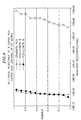
- FIG. 3 is a Weibull plot commonly used for displaying a non-normal distribution of data samples and shows the measured resistance after HTHP processing of a semiconductive PCD layer, as compared to standard PCD, as above. Conventional resistance measurements were made using probes spaced about 1 cm apart on the sample surface, in all cases.
- Sample 1 is PCD formed by adding 2.0 weight percent of boron to a layer of diamond powder including conventional Type I (insulating) diamond grit feedstock, then sintering to convert at least some of the insulative diamond crystals to include a semiconductive surface layer.
- FIG, 3 also shows Sample 2 which is PCD formed by adding 0.5 weight percent of boron to a layer of conventional diamond powder including conventional Type I diamond grit feedstock, then sintering to convert at least some of the insulative diamond crystals to include a semiconductive surface layer.
- Sample 1 and Sample 2 are PCD materials that include a cobalt matrix material at about 10% by weight.
- the standard PCD sample is a conventional PCD material that is substantially similar to Samples 1 and 2, except that the standard PCD material is formed only with conventional, insulative diamonds. As illustrated in FIG. 3, the two PCD samples of present invention exhibit a reduced resistance.
- FIG. 4 is another Weibull plot of measured electrical resistance of the PCD material samples used in FIG. 1, after removal of substantially all of the cobalt matrix phase of such samples by acid leaching.
- acid leaching was intentionally caused for data gathering purposes, by boiling in hydrofluoric acid and nitric acid, but other exemplary techniques may be used alternatively.
- Similar acid leaching of the cobalt matrix phase from the PCD also occurs as a result of the cooling and dielectric fluids used in conventional EDM and EDG cutting operations which can leach out any metal binder material present in the PCD material.
- FIG. 4 is representative of PCD material during EDM and EDG cutting operations.
- FIG. 4 shows a difference of several orders of magnitude in resistance between each of Sample 1 and Sample 2 of the present invention, and standard PCD. Each of the standard PCD and Samples 1 and 2 were substantially free of metal binder materials when the measurements plotted in FIG. 4 were made.
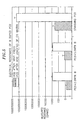
- FIG. 5 is a bar graph summarizing the electrical resistance measurements shown in FIGS. 3 and 4.
- FIG. 5 shows that, after sintering and prior to leaching, each of PCD Samples 1 and 2 have a measured resistance of about 10 ohms, while the standard PCD sample has a measured resistance of about 400-500 ohms.
- Sample 1 has a measured resistance of about 8 ohms
- Sample 2 has a measured resistance of about 20 ohms, i.e. both samples have a resistance less than 50 ohms.
- each of the semiconductive PCD samples exhibit a resistance of less than 10%, and more specifically less than about 5%, of the corresponding resistance of a substantially similar PCD layer formed only of Type I or other conventional insulative diamonds.
- Samples 1 and 2 both exhibit a measured resistance of about 1000 ohms, whereas the standard PCD has a resistance of about 2-3 x 10 8 ohms. The increase in resistance due to acid leaching is much more significant in the standard PCD as compared to Samples 1 and 2,
- semiconductive PCD material of the present invention formed using diamond grit feedstock consisting of Li-, Be- or Al-doped diamond crystals and without the addition of metal binder materials, will exhibit an even greater improvement in resistance/conductivity characteristics, than the PCD layers formed to initially include metal binder materials and from which the metal binder materials are subsequently removed by leaching (as illustrated in FIGS. 4 and 5), when compared to PCD material consisting only of conventional diamonds. Applicant believes that the absence of the additive impurity species used to convert conventional PCD to semiconductive PCD, provides superior diamond crystal-to-diamond crystal bonding.
- Figures 3-5 and Samples 1 and 2 are provided to be illustrative of the advantages of the present invention. Samples 1 and 2 are exemplary only and the reduced resistance advantage of the semiconductive PCD materials of the present invention is similarly achievable for samples formed having different metal binder materials and samples having binder materials present in different percentages.
- the semiconductive PCD material of the present invention (i.e., a PCD layer with at least some Al-doped, Be-doped or Li-doped diamond crystals, or at least some diamond crystals having semiconductive surfaces), also has a much greater thermal conductivity than conventional PCD. Applicants believe that the thermal conductivity of the semiconductive PCD material of the present invention may be 15 times greater than the conductivity of conventional PCD material at 80°K and 4-5 times greater than the conductivity of conventional PCD material at room temperature. When used as a cutting layer in a cutting tool, a semiconductive PCD material is better able to conduct the heat generated by the abrasion of the PCD cutting layer against the object being cut, and thus maintain a lower temperature on the cutting layer. Increased temperatures on the cutting layer and the tool are known to decrease the life of the cutting tool. Consequently, the use of the semiconductive PCD of the present invention as a cutting layer, will provide an increased operating life of the cutting element.
Description
- This invention relates to polycrystalline diamond and more specifically to semiconductive polycrystalline diamond that exhibits enhanced cuttability, especially Electro-Discharge Machining or Electro-Discharge Grinding cuttability.
- Polycrystalline diamond (PCD) materials known in the art are typically formed from diamond grains or crystals and a ductile metal catalyst/binder, and are synthesized by high temperature/high pressure ("HTHP") processes. Such PCD materials are ultra hard materials well known for their mechanical property of high wear resistance, making them a popular material choice for use in such industrial applications as cutting tools for machining, and subterranean mining and drilling, where the mechanical property of wear resistance is highly desired. In such applications, conventional PCD materials can be provided in the form of a surface coating, e.g., on inserts used with cutting and drilling tools, to improve wear resistance of the insert. Traditionally, PCD inserts used in such applications are produced by forming one or more layers of PCD-based material over a suitable substrate material. Such inserts, also referred to as cutting elements, comprise a substrate, a PCD surface layer, and optionally one or more transition layers to improve the bonding between the exposed PCD surface layer and the underlying substrate support layer. Substrates used in such insert applications are commonly formed from a carbide material such as tungsten carbide, WC, cemented with cobalt, Co, and commonly referred to as a cemented tungsten carbide, WC/Co system.
- The layer or layers of PCD conventionally may include a metal binder therein. The metal binder is used to facilitate intercrystalline bonding between diamond grains, and acts to bond the layers to each other and to the underlying substrate. The metal binder material is generally included at a weight percentage of about 10% by weight. Metals conventionally employed as the binder are often selected from the group including cobalt, iron, or nickel and/or mixtures or alloys thereof. The binder material may also include metals such as manganese, tantalum, chromium and/or mixtures or alloys thereof. The metal binder may be provided in powder form as an ingredient for forming the PCD material, or can be drawn into the PCD material from the substrate material during HTHP processing also referred to as the "sintering" process.
- The amount of binder material that is used to form PCD materials represents a compromise between the desired material properties of toughness and hardness/wear resistance. While a higher metal binder content typically increases the toughness of the resulting PCD material, higher metal content also decreases the PCD material hardness, wear resistance and thermal stability. Thus, these inversely affected desired properties ultimately limit the flexibility of being able to provide PCD coatings having desired levels of both wear resistance and toughness to meet the service demands of particular applications. Additionally, when the PCD composition is chosen to increase the wear resistance of the PCD material, typically brittleness also increases, thereby reducing the toughness of the PCD material.
- In many instances, after the PCD is formed, it must be cut to desired shapes for use in a cutting tool. Cutting is typically accomplished using Electro-Discharge Machining (EDM) or Electro-Discharge Grinding (EDG) operations which are well known in the art. However, because of the insulating nature of the diamond skeleton in conventional PCD it is essential to have a metallic matrix material present at the cut to ensure some conductivity of the PCD, essential to the aforementioned cutting operations. The metal binder in the PCD forms a metallic matrix and provides conductivity that supports EDM or EDG cutting. However, cooling fluid or dielectric fluid used for cooling during EDM or EDG cutting, may leach out the metal matrix from the PCD and significantly increase the resistance of the PCD layer. Various cooling/dielectric solutions such as Adcool™, and other corrosion inhibiting solutions and/or deionized water may be used during the EDM or EDG process. The electrical arcing produced between the cutting surface and the wire in EDM operations, and the grinding wheel in EDG operations, also causes leaching.
- If the resistance of the PCD increases significantly due to the metal matrix in the PCD leaching out, or if areas with relatively little metal matrix are encountered, very slow or zero cutting rates may result and breakage of the cutting wire incorporated in the EDM process may occur. In some instances extra metal is provided in the PCD material to overcome this problem. Adding additional metal results in lower thermal stability of the PCD as well as reduced material harness and a correspondingly reduced wear resistance.
- An article in Manufacturing Engineering 104(2), 91(1990) entitled advancing the art of PCD tool grinding describes a three step process for manufacturing PCD tools and a machine that combines electrical discharge erosion and grinding.
- Thus, a PCD material is desired that has enhanced EDM and EDG cuttability without a reduction in material hardness, wear resistance and thermal stability.
- The present invention is directed to a polycrystalline diamond (PCD) ultra hard material and a method for forming the same. In one embodiment, the polycrystalline diamond ultra hard material includes semiconductive diamond crystals therein. The semiconductive diamond crystals may be diamond crystals doped with lithium, beryllium or aluminum. In another exemplary embodiment, the polycrystalline diamond ultra hard material is formed of conventional diamond crystals, at least some of which include semiconductive outer surface layers. According to either of the aforementioned exemplary embodiments, the polycrystalline diamond ultra hard material is a semiconductor material.
- According to one aspect of the present invention there is provided a method for forming a cutting element comprising:
- providing a layer of diamond powder comprising non-conductive diamond crystals and an additive; and
- sintering said layer to convert said non-conductive diamond crystals and said additive to a polycrystalline diamond layer, said polycrystalline diamond layer being a solid semiconductor material.
-
- According to another aspect of the present invention there is provided a semiconductive polycrystalline diamond material formed by sintering comprising diamond crystals doped with a material selected from the group consisting of Be, Li and Al.
- According to one exemplary method of the present invention, a cutting element is formed by providing a substrate and forming a polycrystalline diamond layer over the substrate. The polycrystalline diamond layer is formed over the substrate by providing a layer of diamond powder comprising non-conductive diamond grit feedstock and an additive, and converting the layer of diamond powder to polycrystalline diamond that is a solid semiconductor material. The additive may be chosen from the group consisting of lithium, beryllium, boron, and aluminum. Diamond grit feedstock composed of conventional, insulative diamond crystals, for example Type I diamond crystals, may be used.
- According to another exemplary method of the present invention, a cutting element is formed by providing a layer of diamond grit feedstock including diamond crystals doped with at least one of beryllium, lithium and aluminum, then sintering to convert the layer of diamond grit feedstock to a semiconductive, solid polycrystalline diamond layer.
- According to either of the exemplary methods of formation, the ultra hard PCD layer is formed as a semiconductor material with increased conductivity compared to PCD layers formed of conventional insulative diamond crystals, such as Type I diamond crystals. Even if all the metal binder materials that may be included in the PCD layer are removed by leaching, the cuttability of the semiconductive PCD material of the present invention is enhanced, especially EDM and EDG cuttability.
- The invention is best understood from the following detailed description when read in conjunction with the accompanying drawings. It is emphasized that, according to common practice, the various features of the drawing are not to scale. On the contrary, the dimensions of the various features may be arbitrarily expanded or reduced for clarity. Like numerals denote like features throughout the specification and drawings. Included are the following figures:
- FIG.1 is a perspective view of a cutting element according to an exemplary embodiment of the present invention;
- FIG. 2 is a perspective view of a bit body outfitted with exemplary embodiment cutting elements of the present invention shown in FIG. 1;
- FIG 3 is a graphical representation showing the effects of diamond crystals having semiconductive surface layers, within PCD material according to an exemplary embodiment of the invention
- FIG, 4 is another graphical representation showing the effects of diamond crystals having semiconductive surface layers, within PCD material according to an exemplary embodiment of the invention; and
- FIG. 5 is a graphical representation showing a comparison between conventional PCD material and exemplary semiconductive PCD materials formed according to an exemplary embodiment of the present invention.
-
- A PCD material having enhanced cuttability, especially EDM and EDG cuttability without comprising its hardness, wear resistance, or thermal stability, cutting and other tools incorporating such material, and a method of making such material and tools, are provided. An exemplary embodiment PCD material of the present invention has a substantial percentage of diamond crystals that are semiconductive in nature or which include semiconductive outer surface layers. Such diamond crystals contain small quantities of interstitial impurities such as lithium (Li), beryllium (Be), boron (B), and aluminum (Al) that are sufficient to make them semiconductors.
- Semiconductive diamonds are discussed in Wentorf, R.H. and Bovenkirk, H.P., "Preparation of Semiconducting Diamonds," J. Chem. Phys. 36, p. 1987 (1962); Field, J.E., "The Properties of Diamond." Academic Press, 1979; and, Wentorf, R. H., "The formation of Diamond at High Pressure", in Advances in High Pressure Research, Academic Press, p249-281 (1974). On the other hand, PCD formed with conventional diamond crystals that are electrical insulators, includes a much higher resistance than the PCD of the present invention. This is true both for PCD materials which include metal binder materials therein, and PCD materials void of such metal binder materials.
- An exemplary embodiment PCD of the present invention is formed by using semiconductive diamond grit feedstock formed of semiconductive diamond crystals doped with Li, Be or Al or combinations thereof. In another exemplary embodiment of the present invention, PCD may be formed by using a combination of semiconductive and conventional, non-conductive diamond grit feedstock such as Type I diamond grit feedstock. In yet another exemplary embodiment of the present invention, the PCD is formed using conventional undoped diamond grit feedstock (such as Type I diamond grit feedstock) together with a suitable quantity of additives such as B, Li, Be and Al. The additives diffuse throughout the diamond lattice so as to cause the diamond crystals to transform to diamond crystals that include semiconductive surface layers. This diffusion phenomenon takes place during the HTHP sintering process used to solidify the PCD material. The PCD material formed according to each of the aforementioned methods, is semiconductive in nature. Hereinafter, both the PCD material formed using semiconductive diamond grit feedstock and the PCD material formed using conventional diamond grit feedstock and an additive to convert the diamond crystals to having semiconductive surface layers, will be collectively referred to as semiconductive PCD.
- The semiconductive PCD of the present invention is a solid structural body commonly referred to as an ultra-hard material or ultra-hard layer and may be used as a cutting layer on cutting tools and cutting elements, or a wear resistant layer for other applications. For convenience, cutting elements and cutting tools are referred to as "cutting elements" hereinafter. The semiconductive PCD may be a layer formed over a substrate to produce a cutting element. In an exemplary embodiment, the cutting element may be inserted into a drill bit and used for earth boring. The semiconductive PCD of the present invention may be used in various other applications and industries, in other exemplary embodiments.
- An exemplary cutting element is shown in FIG. 1. FIG. 1
shows cutting element 10 formed ofsubstrate 12 and ultrahard layer 16 which is also referred to as a cutting table and includestop surface 18. Ultrahard layer 16 is formed of semiconductive PCD in the present invention. Interface 14 is formed betweensubstrate 12 and ultrahard layer 16. According to another exemplary embodiment, one or more transition layers (not shown) may be formed between ultrahard layer 16 andsubstrate 12. The generally cylindrically-shaped cutting element illustrated in FIG. 1 is intended to be exemplary only and according to various other exemplary embodiments, the cutting elements and ultra-hard layers may take on any of various other shapes. - In an exemplary embodiment, the cutting element is mounted on a bit such as the drag bit shown in FIG. 2, and contacts the earthen formation along
edge 28, during drilling. In the exemplary embodiment shown in FIG. 2, the cuttingelements 10 are joined to pockets or other receiving shapes that extend intodrag bit body 24 by brazing or other means well known in the art. The illustrated arrangement is intended to be exemplary only and cuttingelements 10 may be used in various other arrangements in other exemplary embodiments. - The method for forming the semiconductive PCD material includes providing a substrate and providing a layer of diamond powderoverthe substrate, then using HTHP processing to sinter, thereby solidifying the layer of diamond powder and converting the same to an ultra-hard layer of PCD, and also bonding the PCD layer to the substrate to form a cutting element. The substrate may be a pre-formed solid substrate, or it may be provided in powder form and also solidified during the sintering operation. The substrate may be formed of various matrix materials. In an exemplary embodiment, the substrate may be formed of cemented tungsten carbide. Cemented tungsten carbide generally refers to tungsten carbide particles disbursed in a substrate binder metal matrix such as iron, nickel, or cobalt. Other substrate materials may be used in other exemplary embodiments. Wear resistant materials suitable for use as the substrate may be selected from compounds of carbide and metals selected from Groups IVB, VB, VIB, and VIIB of the Periodic Table of the Elements. Examples of other such carbides include tantalum carbide and titanium carbide. Substrate binder matrix materials suitable for use in embodiments of the invention include the transition metals of Groups VI, VII, and VII of the Periodic Table of the Elements. For example, iron and nickel are good substrate binder matrix materials.
- The layer of diamond powder used to form a semiconductive PCD material in an exemplary embodiment of the present invention, includes of a plurality of fine diamond crystals. The layer of diamond powder may be provided directly on the substrate or one or more optional transition layers may be provided between the layer of diamond powder and the substrate.
- According to one exemplary embodiment, the layer of diamond powder includes at least some semiconductive diamond grit feedstock consisting of diamond crystals doped with Li, Be, or Al. The semiconductive diamond feedstock may be mixed with conventional, undoped diamond feedstock to form the layer of diamond powder. In another exemplary embodiment, the diamond crystals of the layer of diamond powder may consist substantially only of semiconductive diamond grit feedstock.
- According to another exemplary embodiment, the layer of diamond powder may consist of conventional diamond crystals that are insulators such as, for example, Type I diamond crystals. According to this exemplary embodiment, an additive such as Li, Be, B or Al is added to the layer of diamond powder. The additives may be in powder or granular form and are mixed throughout the layer of diamond powder. In an exemplary embodiment, the additives may be mixed in uniformly throughout the diamond powder layer. The additives are chosen to be small enough to diffuse into the diamond lattice formed as the layer of diamond powder solidifies to form the PCD layer. Because of the small size of the diamond lattice in PCD, the lattice can only accommodate a limited number of impurity species (i.e., additives) for transforming the conventional, insulating diamond crystals to semiconductive diamond crystals. Li, Be, B and Al are elements that are known to be small enough to diffuse into the diamond lattice. Such are intended to be exemplary only and other impurity atoms or compounds may be used in other exemplary embodiments. Li, Be, B and Al make the PCD a P-Type semiconductor.
- The quantity of additive included in the layer of diamond powder ranges from 0.1 wt% to 10.0 wt% in an exemplary embodiment, but other weight percentages may be used in other exemplary embodiments. The upper limit of additive weight percentage is determined by the amount above which the sintering process is adversely affected. An appropriate quantity of suitably small elements or compounds of additives are chosen so that the additives diffuse into and throughout the diamond lattice and cause the insulating diamond crystals to transform to semiconductive diamond crystals. It has been found that a very small amount of the additives can convert the diamond crystals and achieve an improvement of increased conductivity. During the transformation of the insulating diamond material to a semiconductive material, some or all of the diamond crystals are converted to diamond crystals having a semiconductive surface due to diffusion of the additive, This diffusion phenomenon takes place during the HTHP sintering process used to solidify the PCD, during which the additive species are free to diffuse throughout the PCD. It is not necessary to obtain full conversion of the entire diamond crystal to a semiconductive diamond crystal in order to realize a significant conductivity improvement. Rather, the transformation of the surface layer of the diamond crystals to semiconductive surface layers, improves the conductivity and, hence, cuttability of the formed PCD. According to this embodiment, undoped diamond crystals, such as Type I diamond crystals, are converted to diamond crystals that include semiconductive surface layers.
- According to either of the aforementioned exemplary methods of formation, an ultra-hard material of semiconductive PCD is produced. According to either of the exemplary embodiments, sufficient metal binder material may be included in the layer of diamond powder to produce a metal binder material within the PCD material at a volume percentage of up to about 30%, but other volume percentages of binder material may be used in other exemplary embodiments. According to another exemplary embodiment, the metal binder material may diffuse into the PCD layer from the substrate, during the HTHP sintering operation. In an exemplary embodiment, the weight percentage for metal binders may range from 8 -12% by weight and it is common for a weight percentage of no greater than 15% to be used. Metals such as cobalt, iron, nickel, manganese, tantalum, chromium and/or mixtures or alloys thereof may be used as a metal binder material. The metal binder material facilitates intercrystalline bonding between the diamond grains of the PCD layer, acts to bond the PCD layer to other layers or the substrate, and increases the conductivity of the PCD layer. An aspect of the present invention, however, is that because of the conductive nature of the diamond skeleton in the semiconductive PCD formed with semiconductive diamond crystals or diamond crystals having a semiconductive surface layer, it is not necessary to have a metal matrix present to ensure cuttability.
- According to the various embodiments of the present invention, the PCD material has a conductivity sufficiently high to enable cutting using EDM and EDG, even when the PCD was formed without a metal binder or after the metal matrix material has essentially been completely removed by leaching. In one exemplary embodiment, PCD of the present invention that is substantially free of metal binders, was formed to have a resistance of less than 1000 ohms. In another embodiment, the PCD layer formed with a metal binder therein at a weight percentage no greater than 10%, had a resistance of less than 50 ohms.
- The resistance values recited herein, are conventional resistance measurements made using probes spaced about 1 cm apart on the sample surface.
- After the solid semiconductive PCD is formed, an Electro-Discharge Machining or Electro-Discharge Grinding cutting operation may be required to cut the PCD to a desired shape. Increased cutting rates can be achieved on such semiconductive PCD materials using EDM and EDG due to the semiconductive nature of the PCD. This is true even though the cooling and dielectric fluids used throughout the EDM and EDG processes, and the electrical arcs produced by the EDM and EDG processes themselves, leach any metal binder material from the semiconductive PCD during the cutting operation. Even if the metal binder is lost due to leaching, or if metal binder materials are not included at all, applicant has discovered that the PCD of the present invention is sufficiently conductive to ensure cuttability in Electro-Discharge Machining and Electro-Discharge Grinding cutting operations. The semiconductive PCD further includes a very high abrasion resistance while still retaining its cuttability. Since the addition of metal binder material can be reduced or even eliminated, the hardness, wear resistance and thermal stability of the formed PCD layer is not compromised and may be improved.
- After the solid semiconductive PCD is cut to form a cutting element, the cutting element may be joined to a drill bit body by brazing or other means well known in the art.
- FIGS. 3-5 are graphical representations showing the advantages of exemplary semiconductive PCD formed according to embodiments of the present invention. FIGS. 3-5 collectively show that the semiconductive PCD formed according to the present invention includes a significantly lower resistance, i.e., a significantly higher conductivity, than standard PCD material. The figures also show that, after acid leaching of the metal matrix material during the cutting process, the semiconductive PCD of the present invention also exhibits a significantly reduced resistance (i.e., increased conductivity) with respect to standard PCD formed of conventional, insulative diamonds. FIGS. 3-5 also show that the effect of acid leaching during the cutting process, is suppressed in semiconductive PCD formed according to the present invention, in comparison to standard PCD. "Standard PCD" consists of conventional insulative diamonds, such as Type I diamonds.
- FIG. 3 is a Weibull plot commonly used for displaying a non-normal distribution of data samples and shows the measured resistance after HTHP processing of a semiconductive PCD layer, as compared to standard PCD, as above. Conventional resistance measurements were made using probes spaced about 1 cm apart on the sample surface, in all cases. In FIG. 3,
Sample 1 is PCD formed by adding 2.0 weight percent of boron to a layer of diamond powder including conventional Type I (insulating) diamond grit feedstock, then sintering to convert at least some of the insulative diamond crystals to include a semiconductive surface layer. FIG, 3 also shows Sample 2 which is PCD formed by adding 0.5 weight percent of boron to a layer of conventional diamond powder including conventional Type I diamond grit feedstock, then sintering to convert at least some of the insulative diamond crystals to include a semiconductive surface layer. Each ofSample 1 and Sample 2 are PCD materials that include a cobalt matrix material at about 10% by weight. The standard PCD sample is a conventional PCD material that is substantially similar toSamples 1 and 2, except that the standard PCD material is formed only with conventional, insulative diamonds. As illustrated in FIG. 3, the two PCD samples of present invention exhibit a reduced resistance. - FIG. 4 is another Weibull plot of measured electrical resistance of the PCD material samples used in FIG. 1, after removal of substantially all of the cobalt matrix phase of such samples by acid leaching. In the examples used to provide the data shown in FIG. 4, acid leaching was intentionally caused for data gathering purposes, by boiling in hydrofluoric acid and nitric acid, but other exemplary techniques may be used alternatively. Similar acid leaching of the cobalt matrix phase from the PCD also occurs as a result of the cooling and dielectric fluids used in conventional EDM and EDG cutting operations which can leach out any metal binder material present in the PCD material. As such, FIG. 4 is representative of PCD material during EDM and EDG cutting operations. FIG. 4 shows a difference of several orders of magnitude in resistance between each of
Sample 1 and Sample 2 of the present invention, and standard PCD. Each of the standard PCD andSamples 1 and 2 were substantially free of metal binder materials when the measurements plotted in FIG. 4 were made. - FIG. 5 is a bar graph summarizing the electrical resistance measurements shown in FIGS. 3 and 4. FIG. 5 shows that, after sintering and prior to leaching, each of
PCD Samples 1 and 2 have a measured resistance of about 10 ohms, while the standard PCD sample has a measured resistance of about 400-500 ohms. In particular, after HTHP processing,Sample 1 has a measured resistance of about 8 ohms and Sample 2 has a measured resistance of about 20 ohms, i.e. both samples have a resistance less than 50 ohms. As formed, then, it can be seen that each of the semiconductive PCD samples exhibit a resistance of less than 10%, and more specifically less than about 5%, of the corresponding resistance of a substantially similar PCD layer formed only of Type I or other conventional insulative diamonds. After leaching substantially all metal binder material fromSamples 1 and 2 of the present invention,Samples 1 and 2 both exhibit a measured resistance of about 1000 ohms, whereas the standard PCD has a resistance of about 2-3 x 10⁸ ohms. The increase in resistance due to acid leaching is much more significant in the standard PCD as compared toSamples 1 and 2, - It is believed that semiconductive PCD material of the present invention formed using diamond grit feedstock consisting of Li-, Be- or Al-doped diamond crystals and without the addition of metal binder materials, will exhibit an even greater improvement in resistance/conductivity characteristics, than the PCD layers formed to initially include metal binder materials and from which the metal binder materials are subsequently removed by leaching (as illustrated in FIGS. 4 and 5), when compared to PCD material consisting only of conventional diamonds. Applicant believes that the absence of the additive impurity species used to convert conventional PCD to semiconductive PCD, provides superior diamond crystal-to-diamond crystal bonding.
- Figures 3-5 and
Samples 1 and 2 are provided to be illustrative of the advantages of the present invention.Samples 1 and 2 are exemplary only and the reduced resistance advantage of the semiconductive PCD materials of the present invention is similarly achievable for samples formed having different metal binder materials and samples having binder materials present in different percentages. - The semiconductive PCD material of the present invention (i.e., a PCD layer with at least some Al-doped, Be-doped or Li-doped diamond crystals, or at least some diamond crystals having semiconductive surfaces), also has a much greater thermal conductivity than conventional PCD. Applicants believe that the thermal conductivity of the semiconductive PCD material of the present invention may be 15 times greater than the conductivity of conventional PCD material at 80°K and 4-5 times greater than the conductivity of conventional PCD material at room temperature. When used as a cutting layer in a cutting tool, a semiconductive PCD material is better able to conduct the heat generated by the abrasion of the PCD cutting layer against the object being cut, and thus maintain a lower temperature on the cutting layer. Increased temperatures on the cutting layer and the tool are known to decrease the life of the cutting tool. Consequently, the use of the semiconductive PCD of the present invention as a cutting layer, will provide an increased operating life of the cutting element.
- The scope of the present invention is not intended to be limited to the exemplary embodiments shown and described herein. Rather, the scope of the present invention is embodied by the appended claims.
Claims (13)
- A method for forming a cutting element comprising:providing a layer of diamond powder comprising non-conductive diamond crystals and an additive; andsintering said layer to convert said non-conductive diamond crystals and said additive to a polycrystalline diamond layer, said polycrystalline diamond layer being a solid semiconductor material.
- A method as claimed in claim 1, wherein said sintering includes forming semiconductive surface layers on a plurality of said non-conductive diamond crystals.
- A method as claimed in claim 1 or 2, wherein said additive comprises boron.
- A method as claimed in claim 1 or 2, wherein said additive comprises at least one of Li, Be, and Al.
- A method as claimed in any one of the preceding claims, wherein said non-conductive diamond crystals substantially comprise Type I diamond grit feedstock.
- A method as claimed in claim 1, wherein said additives are selected from the group of additives consisting of Be, Li and Al.
- A method as claimed in claim 6, wherein said providing a layer of diamond powder comprises providing a layer of diamond grit feedstock that consists substantially only of said diamond crystals doped with at least one of Be, Li and Al.
- A semiconductive polycrystalline diamond material formed by sintering comprising diamond crystals doped with a material selected from the group consisting of Be, Li and A1.
- A semiconductive polycrystalline diamond material as claimed in claim 8, wherein said polycrystalline diamond material is characterized as being a P-type semiconductor material.
- A semiconductive polycrystalline diamond material as claimed in claim 8, wherein the diamond crystals are Type I diamond crystals and wherein, a plurality of said Type 1 diamond crystals have a semiconductive surface layer.
- A polycrystalline diamond material as claimed in claim 10, in which said polycrystalline diamond material further includes impurity species therein, said impurity species selected from the group consisting of Li, Be, B, and Al.
- A polycrystalline diamond material as claimed in claim 10 or 11, in which said semiconductive surface layers include impurity species therein, said impurity species selected form the group consisting of Li, Be, B, and A1.
- A polycrystalline diamond material as claimed in any one of claims 10 to 12, wherein said polycrystalline diamond material is a P-type semiconductive material.
Priority Applications (1)
| Application Number | Priority Date | Filing Date | Title |
|---|---|---|---|
| EP05076331A EP1602478B1 (en) | 2002-02-26 | 2003-02-26 | Cutting element including semiconductive polycrystalline diamond |
Applications Claiming Priority (2)
| Application Number | Priority Date | Filing Date | Title |
|---|---|---|---|
| US35963002P | 2002-02-26 | 2002-02-26 | |
| US359630P | 2002-02-26 |
Related Child Applications (1)
| Application Number | Title | Priority Date | Filing Date |
|---|---|---|---|
| EP05076331A Division EP1602478B1 (en) | 2002-02-26 | 2003-02-26 | Cutting element including semiconductive polycrystalline diamond |
Publications (3)
| Publication Number | Publication Date |
|---|---|
| EP1340737A2 EP1340737A2 (en) | 2003-09-03 |
| EP1340737A3 EP1340737A3 (en) | 2004-04-07 |
| EP1340737B1 true EP1340737B1 (en) | 2005-10-12 |
Family
ID=27734770
Family Applications (1)
| Application Number | Title | Priority Date | Filing Date |
|---|---|---|---|
| EP03251153A Expired - Fee Related EP1340737B1 (en) | 2002-02-26 | 2003-02-26 | Semiconductive polycrystalline diamond |
Country Status (6)
| Country | Link |
|---|---|
| US (2) | US6846341B2 (en) |
| EP (1) | EP1340737B1 (en) |
| JP (2) | JP4624649B2 (en) |
| CA (1) | CA2419709C (en) |
| DE (2) | DE60301807T2 (en) |
| ZA (1) | ZA200301565B (en) |
Families Citing this family (44)
| Publication number | Priority date | Publication date | Assignee | Title |
|---|---|---|---|---|
| US7517588B2 (en) * | 2003-10-08 | 2009-04-14 | Frushour Robert H | High abrasion resistant polycrystalline diamond composite |
| US7595110B2 (en) * | 2003-10-08 | 2009-09-29 | Frushour Robert H | Polycrystalline diamond composite |
| EP1706238A1 (en) * | 2004-01-06 | 2006-10-04 | Element Six Limited | Tool insert |
| KR101091887B1 (en) * | 2004-09-13 | 2011-12-12 | 신승도 | Transparent diamodnd like carbon coating with high conductivity and fabrication method thereof |
| JP2006152424A (en) * | 2004-12-01 | 2006-06-15 | Osg Corp | Hard film, and hard film-coated cutting tool |
| US7350601B2 (en) | 2005-01-25 | 2008-04-01 | Smith International, Inc. | Cutting elements formed from ultra hard materials having an enhanced construction |
| EP2400531A3 (en) * | 2005-06-20 | 2012-03-28 | Nippon Telegraph And Telephone Corporation | Diamond semiconductor element and process for producing the same |
| US8142261B1 (en) | 2006-11-27 | 2012-03-27 | Chien-Min Sung | Methods for enhancing chemical mechanical polishing pad processes |
| US7749050B2 (en) * | 2006-02-06 | 2010-07-06 | Chien-Min Sung | Pad conditioner dresser |
| US20100173567A1 (en) * | 2006-02-06 | 2010-07-08 | Chien-Min Sung | Methods and Devices for Enhancing Chemical Mechanical Polishing Processes |
| US7628234B2 (en) | 2006-02-09 | 2009-12-08 | Smith International, Inc. | Thermally stable ultra-hard polycrystalline materials and compacts |
| JP2008087088A (en) * | 2006-09-29 | 2008-04-17 | Denso Corp | Cutting tool and manufacturing method of the same |
| US8028771B2 (en) | 2007-02-06 | 2011-10-04 | Smith International, Inc. | Polycrystalline diamond constructions having improved thermal stability |
| US7942219B2 (en) | 2007-03-21 | 2011-05-17 | Smith International, Inc. | Polycrystalline diamond constructions having improved thermal stability |
| US20090127231A1 (en) * | 2007-11-08 | 2009-05-21 | Chien-Min Sung | Methods of Forming Superhard Cutters and Superhard Cutters Formed Thereby |
| US9297211B2 (en) | 2007-12-17 | 2016-03-29 | Smith International, Inc. | Polycrystalline diamond construction with controlled gradient metal content |
| US8663349B2 (en) | 2008-10-30 | 2014-03-04 | Us Synthetic Corporation | Polycrystalline diamond compacts, and related methods and applications |
| CA2688960A1 (en) * | 2008-12-17 | 2010-06-17 | David Ballantyne | Multi-element diamond reference standard |
| US8210287B1 (en) | 2009-01-05 | 2012-07-03 | Diamond Products, Limited | Mining core drill bit and method of making thereof |
| US20100192474A1 (en) | 2009-01-30 | 2010-08-05 | Lehigh University | Ultrahard stishovite nanoparticles and methods of manufacture |
| SA110310235B1 (en) * | 2009-03-31 | 2014-03-03 | بيكر هوغيس انكوربوريتد | Methods for Bonding Preformed Cutting Tables to Cutting Element Substrates and Cutting Element Formed by such Processes |
| US8079786B2 (en) * | 2009-04-22 | 2011-12-20 | Corbin Manufacturing, Inc. | Tool insert blanks and method of manufacture |
| WO2010129813A2 (en) * | 2009-05-06 | 2010-11-11 | Smith International, Inc. | Methods of making and attaching tsp material for forming cutting elements, cutting elements having such tsp material and bits incorporating such cutting elements |
| WO2010148313A2 (en) | 2009-06-18 | 2010-12-23 | Smith International, Inc. | Polycrystalline diamond cutting elements with engineered porosity and method for manufacturing such cutting elements |
| US8771391B2 (en) | 2011-02-22 | 2014-07-08 | Baker Hughes Incorporated | Methods of forming polycrystalline compacts |
| US9403215B2 (en) | 2011-04-11 | 2016-08-02 | Sumitomo Electric Industries, Ltd. | Cutting tool and method for producing same |
| US8741010B2 (en) | 2011-04-28 | 2014-06-03 | Robert Frushour | Method for making low stress PDC |
| US8858665B2 (en) | 2011-04-28 | 2014-10-14 | Robert Frushour | Method for making fine diamond PDC |
| US8974559B2 (en) | 2011-05-12 | 2015-03-10 | Robert Frushour | PDC made with low melting point catalyst |
| US9061264B2 (en) | 2011-05-19 | 2015-06-23 | Robert H. Frushour | High abrasion low stress PDC |
| US8828110B2 (en) | 2011-05-20 | 2014-09-09 | Robert Frushour | ADNR composite |
| US8833635B1 (en) | 2011-07-28 | 2014-09-16 | Us Synthetic Corporation | Method for identifying PCD elements for EDM processing |
| US9482056B2 (en) | 2011-12-30 | 2016-11-01 | Smith International, Inc. | Solid PCD cutter |
| CA2825729C (en) | 2012-11-21 | 2018-05-22 | Diamond Products, Limited | Diamond mining core drill bit and methods of making thereof |
| CA2854691C (en) | 2013-07-03 | 2017-10-31 | Karl H. Moller | Method of making diamond mining core drill bit and reamer |
| GB2554569A (en) | 2015-06-03 | 2018-04-04 | Halliburton Energy Services Inc | Electrochemical removal of metal or other material from polycrystalline diamond |
| US10287824B2 (en) | 2016-03-04 | 2019-05-14 | Baker Hughes Incorporated | Methods of forming polycrystalline diamond |
| US11396688B2 (en) | 2017-05-12 | 2022-07-26 | Baker Hughes Holdings Llc | Cutting elements, and related structures and earth-boring tools |
| US11292750B2 (en) | 2017-05-12 | 2022-04-05 | Baker Hughes Holdings Llc | Cutting elements and structures |
| US11536091B2 (en) | 2018-05-30 | 2022-12-27 | Baker Hughes Holding LLC | Cutting elements, and related earth-boring tools and methods |
| CN113710984A (en) * | 2019-11-26 | 2021-11-26 | 住友电气工业株式会社 | Measuring tool having tip portion made of polycrystalline diamond |
| TWI735227B (en) * | 2020-05-11 | 2021-08-01 | 國立臺北科技大學 | Composite polycrystalline diamond flake, composition and manufacturing method thereof |
| JP7359522B2 (en) | 2020-11-30 | 2023-10-11 | 住友電工ハードメタル株式会社 | Sintered bodies and cutting tools |
| WO2023228324A1 (en) | 2022-05-25 | 2023-11-30 | 住友電工ハードメタル株式会社 | Sintered body and cutting tool |
Family Cites Families (18)
| Publication number | Priority date | Publication date | Assignee | Title |
|---|---|---|---|---|
| US3141855A (en) * | 1961-08-31 | 1964-07-21 | Gen Electric | Method for and product produced by the introduction of boron atoms into the surface of diamond crystals |
| US3268457A (en) * | 1962-04-05 | 1966-08-23 | Armando A Giardini | Method of creating electrically semiconducting diamond |
| US3735321A (en) * | 1971-06-18 | 1973-05-22 | Gen Electric | Thermistor |
| US4268276A (en) * | 1978-04-24 | 1981-05-19 | General Electric Company | Compact of boron-doped diamond and method for making same |
| JPS58199776A (en) * | 1982-05-12 | 1983-11-21 | 住友電気工業株式会社 | Diamond sintered body for tool and manufacture |
| US4907377A (en) * | 1988-06-16 | 1990-03-13 | General Electric Company | Directional catalyst alloy sweep through process for preparing diamond compacts |
| WO1990001986A1 (en) * | 1988-08-17 | 1990-03-08 | The Australian National University | Diamond compact possessing low electrical resistivity |
| JP2719163B2 (en) * | 1989-01-26 | 1998-02-25 | 昭和電工株式会社 | Manufacturing method of single crystal diamond |
| JP2695000B2 (en) | 1989-04-11 | 1997-12-24 | 住友電気工業株式会社 | Thermistor and manufacturing method thereof |
| US5099296A (en) * | 1990-04-06 | 1992-03-24 | Xerox Corporation | Thin film transistor |
| US5266236A (en) * | 1991-10-09 | 1993-11-30 | General Electric Company | Thermally stable dense electrically conductive diamond compacts |
| US5213248A (en) * | 1992-01-10 | 1993-05-25 | Norton Company | Bonding tool and its fabrication |
| JPH06263595A (en) * | 1993-03-10 | 1994-09-20 | Canon Inc | Diamond-coated material and its production |
| US5698328A (en) * | 1994-04-06 | 1997-12-16 | The Regents Of The University Of California | Diamond thin film electron emitter |
| US5567251A (en) * | 1994-08-01 | 1996-10-22 | Amorphous Alloys Corp. | Amorphous metal/reinforcement composite material |
| GB9616043D0 (en) * | 1996-07-31 | 1996-09-11 | De Beers Ind Diamond | Diamond |
| US6045440A (en) * | 1997-11-20 | 2000-04-04 | General Electric Company | Polycrystalline diamond compact PDC cutter with improved cutting capability |
| JPH11292630A (en) * | 1998-04-08 | 1999-10-26 | Ishizuka Kenkyusho:Kk | Diamond-silicon carbide composite sintered compact and its production |
-
2003
- 2003-02-25 US US10/374,373 patent/US6846341B2/en not_active Expired - Lifetime
- 2003-02-25 CA CA002419709A patent/CA2419709C/en not_active Expired - Fee Related
- 2003-02-26 JP JP2003049011A patent/JP4624649B2/en not_active Expired - Fee Related
- 2003-02-26 ZA ZA200301565A patent/ZA200301565B/en unknown
- 2003-02-26 EP EP03251153A patent/EP1340737B1/en not_active Expired - Fee Related
- 2003-02-26 DE DE60301807T patent/DE60301807T2/en not_active Expired - Lifetime
- 2003-02-26 DE DE60329718T patent/DE60329718D1/en not_active Expired - Lifetime
-
2004
- 2004-03-19 US US10/804,297 patent/US20040172885A1/en not_active Abandoned
-
2010
- 2010-08-19 JP JP2010183926A patent/JP5432084B2/en not_active Expired - Fee Related
Also Published As
| Publication number | Publication date |
|---|---|
| CA2419709C (en) | 2008-09-23 |
| EP1340737A3 (en) | 2004-04-07 |
| JP5432084B2 (en) | 2014-03-05 |
| US6846341B2 (en) | 2005-01-25 |
| JP2011025404A (en) | 2011-02-10 |
| JP2003291036A (en) | 2003-10-14 |
| DE60301807T2 (en) | 2006-06-29 |
| ZA200301565B (en) | 2003-09-16 |
| DE60301807D1 (en) | 2006-02-23 |
| US20040172885A1 (en) | 2004-09-09 |
| DE60329718D1 (en) | 2009-11-26 |
| EP1340737A2 (en) | 2003-09-03 |
| JP4624649B2 (en) | 2011-02-02 |
| US20030196385A1 (en) | 2003-10-23 |
| CA2419709A1 (en) | 2003-08-26 |
Similar Documents
| Publication | Publication Date | Title |
|---|---|---|
| EP1340737B1 (en) | Semiconductive polycrystalline diamond | |
| KR900002701B1 (en) | Diamond sintered body for tools and method of manufacturing the same | |
| US10179390B2 (en) | Methods of fabricating a polycrystalline diamond compact | |
| JP5298372B2 (en) | Composite sintered body | |
| EP0155066B1 (en) | Hard diamond sintered body | |
| EP0181258B1 (en) | Improved cubic boron nitride compact and method of making | |
| EP2519369B1 (en) | Polycrystalline diamond compacts, methods of making same, and applications therefor | |
| US6585064B2 (en) | Polycrystalline diamond partially depleted of catalyzing material | |
| AU2017212472B2 (en) | Binder compositions of tungsten tetraboride and abrasive methods thereof | |
| KR20100067657A (en) | Polycrystalline diamond composites | |
| CA2423102C (en) | Polycrystalline diamond with a surface depleted of catalyzing material | |
| KR20110137773A (en) | Polycrystalline diamond | |
| EP2768994A2 (en) | Polycrystalline diamond compacts, related products, and methods of manufacture | |
| CN103451460A (en) | Cubic boron nitride compacts | |
| US20190184524A1 (en) | Polycrystalline diamond construction & method of making | |
| DE60301810T2 (en) | Cable operated disc brake | |
| EP0816304A2 (en) | Ceramic bonded cubic boron nitride compact | |
| EP1602478A2 (en) | Semiconductive polycrystalline diamond | |
| US10227827B2 (en) | Methods of forming polycrystalline diamond compacts and earth-boring tools | |
| JPS6319585B2 (en) | ||
| WO2019046590A1 (en) | Cutting elements and methods for fabricating diamond compacts and cutting elements with functionalized nanoparticles | |
| JPH01242764A (en) | Manufacture of tough cermet tool |
Legal Events
| Date | Code | Title | Description |
|---|---|---|---|
| PUAI | Public reference made under article 153(3) epc to a published international application that has entered the european phase |
Free format text: ORIGINAL CODE: 0009012 |
|
| AK | Designated contracting states |
Kind code of ref document: A2 Designated state(s): AT BE BG CH CY CZ DE DK EE ES FI FR GB GR HU IE IT LI LU MC NL PT SE SI SK TR |
|
| AX | Request for extension of the european patent |
Extension state: AL LT LV MK RO |
|
| PUAL | Search report despatched |
Free format text: ORIGINAL CODE: 0009013 |
|
| RIC1 | Information provided on ipc code assigned before grant |
Ipc: 7C 04B 41/50 B Ipc: 7B 23B 27/14 A Ipc: 7C 04B 41/85 B |
|
| AK | Designated contracting states |
Kind code of ref document: A3 Designated state(s): AT BE BG CH CY CZ DE DK EE ES FI FR GB GR HU IE IT LI LU MC NL PT SE SI SK TR |
|
| AX | Request for extension of the european patent |
Extension state: AL LT LV MK RO |
|
| 17P | Request for examination filed |
Effective date: 20040525 |
|
| 17Q | First examination report despatched |
Effective date: 20040630 |
|
| AKX | Designation fees paid |
Designated state(s): DE GB IE IT |
|
| GRAP | Despatch of communication of intention to grant a patent |
Free format text: ORIGINAL CODE: EPIDOSNIGR1 |
|
| GRAS | Grant fee paid |
Free format text: ORIGINAL CODE: EPIDOSNIGR3 |
|
| GRAA | (expected) grant |
Free format text: ORIGINAL CODE: 0009210 |
|
| AK | Designated contracting states |
Kind code of ref document: B1 Designated state(s): DE GB IE IT |
|
| REG | Reference to a national code |
Ref country code: GB Ref legal event code: FG4D |
|
| REG | Reference to a national code |
Ref country code: IE Ref legal event code: FG4D |
|
| REF | Corresponds to: |
Ref document number: 60301807 Country of ref document: DE Date of ref document: 20060223 Kind code of ref document: P |
|
| PLBE | No opposition filed within time limit |
Free format text: ORIGINAL CODE: 0009261 |
|
| STAA | Information on the status of an ep patent application or granted ep patent |
Free format text: STATUS: NO OPPOSITION FILED WITHIN TIME LIMIT |
|
| 26N | No opposition filed |
Effective date: 20060713 |
|
| PGFP | Annual fee paid to national office [announced via postgrant information from national office to epo] |
Ref country code: IE Payment date: 20140211 Year of fee payment: 12 |
|
| PGFP | Annual fee paid to national office [announced via postgrant information from national office to epo] |
Ref country code: IT Payment date: 20140213 Year of fee payment: 12 |
|
| PGFP | Annual fee paid to national office [announced via postgrant information from national office to epo] |
Ref country code: GB Payment date: 20140226 Year of fee payment: 12 |
|
| PGFP | Annual fee paid to national office [announced via postgrant information from national office to epo] |
Ref country code: DE Payment date: 20140417 Year of fee payment: 12 |
|
| REG | Reference to a national code |
Ref country code: DE Ref legal event code: R119 Ref document number: 60301807 Country of ref document: DE |
|
| GBPC | Gb: european patent ceased through non-payment of renewal fee |
Effective date: 20150226 |
|
| REG | Reference to a national code |
Ref country code: IE Ref legal event code: MM4A |
|
| PG25 | Lapsed in a contracting state [announced via postgrant information from national office to epo] |
Ref country code: IT Free format text: LAPSE BECAUSE OF NON-PAYMENT OF DUE FEES Effective date: 20150226 |
|
| PG25 | Lapsed in a contracting state [announced via postgrant information from national office to epo] |
Ref country code: GB Free format text: LAPSE BECAUSE OF NON-PAYMENT OF DUE FEES Effective date: 20150226 Ref country code: IE Free format text: LAPSE BECAUSE OF NON-PAYMENT OF DUE FEES Effective date: 20150226 Ref country code: DE Free format text: LAPSE BECAUSE OF NON-PAYMENT OF DUE FEES Effective date: 20150901 |