EP1339225A2 - Image pickup apparatus - Google Patents
Image pickup apparatus Download PDFInfo
- Publication number
- EP1339225A2 EP1339225A2 EP03003855A EP03003855A EP1339225A2 EP 1339225 A2 EP1339225 A2 EP 1339225A2 EP 03003855 A EP03003855 A EP 03003855A EP 03003855 A EP03003855 A EP 03003855A EP 1339225 A2 EP1339225 A2 EP 1339225A2
- Authority
- EP
- European Patent Office
- Prior art keywords
- light
- image pickup
- refractive index
- pickup element
- area
- Prior art date
- Legal status (The legal status is an assumption and is not a legal conclusion. Google has not performed a legal analysis and makes no representation as to the accuracy of the status listed.)
- Granted
Links
Images


























Classifications
-
- H—ELECTRICITY
- H10—SEMICONDUCTOR DEVICES; ELECTRIC SOLID-STATE DEVICES NOT OTHERWISE PROVIDED FOR
- H10F—INORGANIC SEMICONDUCTOR DEVICES SENSITIVE TO INFRARED RADIATION, LIGHT, ELECTROMAGNETIC RADIATION OF SHORTER WAVELENGTH OR CORPUSCULAR RADIATION
- H10F39/00—Integrated devices, or assemblies of multiple devices, comprising at least one element covered by group H10F30/00, e.g. radiation detectors comprising photodiode arrays
- H10F39/80—Constructional details of image sensors
- H10F39/806—Optical elements or arrangements associated with the image sensors
-
- H—ELECTRICITY
- H10—SEMICONDUCTOR DEVICES; ELECTRIC SOLID-STATE DEVICES NOT OTHERWISE PROVIDED FOR
- H10F—INORGANIC SEMICONDUCTOR DEVICES SENSITIVE TO INFRARED RADIATION, LIGHT, ELECTROMAGNETIC RADIATION OF SHORTER WAVELENGTH OR CORPUSCULAR RADIATION
- H10F39/00—Integrated devices, or assemblies of multiple devices, comprising at least one element covered by group H10F30/00, e.g. radiation detectors comprising photodiode arrays
- H10F39/80—Constructional details of image sensors
- H10F39/805—Coatings
- H10F39/8053—Colour filters
-
- H—ELECTRICITY
- H10—SEMICONDUCTOR DEVICES; ELECTRIC SOLID-STATE DEVICES NOT OTHERWISE PROVIDED FOR
- H10F—INORGANIC SEMICONDUCTOR DEVICES SENSITIVE TO INFRARED RADIATION, LIGHT, ELECTROMAGNETIC RADIATION OF SHORTER WAVELENGTH OR CORPUSCULAR RADIATION
- H10F39/00—Integrated devices, or assemblies of multiple devices, comprising at least one element covered by group H10F30/00, e.g. radiation detectors comprising photodiode arrays
- H10F39/80—Constructional details of image sensors
- H10F39/806—Optical elements or arrangements associated with the image sensors
- H10F39/8063—Microlenses
-
- H—ELECTRICITY
- H10—SEMICONDUCTOR DEVICES; ELECTRIC SOLID-STATE DEVICES NOT OTHERWISE PROVIDED FOR
- H10F—INORGANIC SEMICONDUCTOR DEVICES SENSITIVE TO INFRARED RADIATION, LIGHT, ELECTROMAGNETIC RADIATION OF SHORTER WAVELENGTH OR CORPUSCULAR RADIATION
- H10F39/00—Integrated devices, or assemblies of multiple devices, comprising at least one element covered by group H10F30/00, e.g. radiation detectors comprising photodiode arrays
- H10F39/80—Constructional details of image sensors
- H10F39/806—Optical elements or arrangements associated with the image sensors
- H10F39/8067—Reflectors
Definitions
- the present invention relates to an image pickup element for picking up an object image.
- Fig. 1 shows a structure of a general image pickup element 61 for forming a color image, which has been used up to now.
- Reference numeral 501 denotes a silicon wafer; 502, a microlens; 503, a photoelectric conversion section having a function for converting a received photon into an electric charge; 504 (504r and 504g), color filters for separating wavelengths of a light; and 510, a Poly wiring layer serving as a gate for controlling an electric charge of the photoelectric conversion section.
- Reference numerals 511 to 513 denote wiring layers made of a metal such as aluminum.
- reference numeral 511 denotes an AL1 wiring layer serving as a connection between respective layers and an output line; 512, an AL2 wiring layer serving as a well power supply line and a control line; and 513, an AL3 wiring layer serving as a light shield and a power supply line.
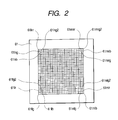
- Fig. 2 is a view of the image pickup element 61 viewed from above.
- Each pixel constituting the image pickup element 61 is provided with a primary color filter of R (red), G (green), or B (blue).
- a color filter there is a complementary color filter which uses three colors of C (cyan), M (magenta), and Y (yellow) as well.
- An image pickup technology is widely used in which: pixels are arranged in a mosaic shape; and then, luminance information and color information corresponding to the number of pixels are created by signal processing.
- a color filter array of the image pickup element 61 used here a structure called a Bayer array is often adopted. In Fig.
- reference symbol 61mng denotes a first green pixel; 61mnb, a blue pixel; 61mnr, a red pixel; and 61mng2, a second green pixel.
- m indicates an array number of a pixel in a horizontal direction and n indicates an array number of a pixel in a vertical direction.
- Fig. 2 the number of green pixels is twice as many as that of blue or red pixels.
- image pickup for obtaining satisfactory image characteristics consists of a first process for forming an object image with an optical apparatus, a second process for adjusting a high frequency component of a spatial frequency characteristic of the object image to suppress the component, a third process for photoelectrically converting the object image whose spatial frequency characteristic has been adjusted, and a fourth process for correcting a response according to a spatial frequency with respect to an obtained electric signal.
- the Nyquist frequency is a frequency that is a half of a sampling frequency depending upon a pixel pitch. Therefore, the optimized series of processes is for obtaining a high quality image, in which aliasing distortion is less conspicuous, that is, moiré is less conspicuous, by adjusting an optical image to be sampled such that it becomes an optical image having a characteristic according to the Nyquist frequency peculiar to the image pickup element.
- a modulation transfer function which is a spatial frequency transmission characteristic of an image, is an evaluation amount with which a characteristic concerning a sharpness of a digital still camera, a video camera, or the like can be represented well.
- Specific factors affecting this MTF are an imaging optical system serving as an optical apparatus, an optical lowpass filter for band limitation of an object image, an opening shape of a photoelectric conversion area of an image pickup element, digital aperture correction, and the like.
- An overall MTF representing a final image characteristic is given as a product of MFTs of the respective factors. That is, it is sufficient to find MTFs of the above-mentioned first to fourth processes and calculate a product of the MTFs.
- the structure for reducing components of the Nyquist frequency or more peculiar to the image pickup element in the spatial frequency characteristic of the optical image means that components of the Nyquist frequency or more are small in the product of MTFs of the first, second, and third processes excluding the fourth process.
- image pickup is performed on the premise that a still image is viewed as in a digital still camera, it is necessary to take into account the fact that an image with a higher resolution is easily obtained when a response in a frequency slightly below the Nyquist frequency is higher even if high frequencies exceeding the Nyquist frequency are not eliminated but remain more or less.
- an optical aberration is easier to be corrected in a center of a screen than in a peripheral part of the screen.
- MTF diffraction limit
- an optical lowpass filter is usually used.
- a material having a birefringent characteristic such as a rock crystal is utilized for the optical lowpass filter.
- a phase-type diffraction grating as disclosed in Japanese Patent Application Laid-Open No. 2000-066141 may be utilized.
- R 2 (u) represents a response
- u represents a spatial frequency of an optical image
- ⁇ represents an object image separation width
- a thickness of the birefringent plate is selected appropriately, it is possible to eliminate the response in the Nyquist frequency of the image pickup element.
- the same effect can be obtained through diffraction by separating the optical image into a plurality of images having a predetermined positional relationship and superimposing the images.
- a CCD image pickup element in which pixels with a primary color filter, which is considered to have a high color reproducibility, are arranged in a mosaic shape, one each of optical filters of R (red), G (green), and B (blue) are arranged between a microlens 2 and a photoelectric conversion area 3.
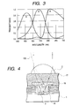
- Fig. 3 shows a spectral transmittance characteristic of R, G, and B color filters in an image pickup element. Since a transmittance of an infrared light is high, an infrared light cut filter for blocking a wavelength of 650 nm or more is actually further laid over these color filters between the image pickup element and an image pickup lens. As it is seen from this, only approximately one third of visible light are used effectively in one pixel.
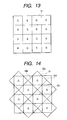
- an area ratio of R, G, and B pixels of a color image pickup element of the Bayer array shown in Fig. 13 is 1/4 : 2/4 : 1/4 in case that an area of one unit constituting a regular array is assumed to be one.
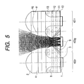
- Fig. 5 shows a result of tracing incident light in the structure described in this patent application.
- Reference numeral 16 denotes a cap layer consisting of resin, which is formed of a material having a refractive index of approximately 1.6.
- Reference numeral 17 denotes a low refractive index layer, which is formed of resin having a refractive index lower than that of the cap layer 16 or formed in hollow (in which the air or an inert gas such as nitrogen is filled). Consequently, since an interface between the cap layer 16 and the low refractive index layer 17 becomes a surface on which light tends to be totally reflected, it is intended to take in oblique-incident light.
- a shape of an incidence section which is the interface between the cap layer 16 formed of a high refractive index material and the low refractive index layer 17 and is on the object side
- an R shape as in Fig. 4 even if a part of oblique-incident light are reflected on the R surface, the light form an angle exceeding a total reflection condition on a surface on the opposite side and directly passes through the R surface to the low refractive index layer 17 as show in the result of tracing light of Fig. 5.
- the light having passed through the R surface may enter an adjacent pixel, which may also become a problem.
- An object of the present invention is to realize an image pickup element in which an efficiency of utilization of incident light is enhanced.
- an image pickup element including: a photoelectric conversion section; a wavelength selection section formed closer to an incident side of light than the photoelectric conversion section, for transmitting light of a predetermined wavelength range; a first area having a predetermined refractive index and being formed closer to the incident side of light than the wavelength selection section; and a second area having a predetermined refractive index and being formed closer to the incident side of light than the first area, wherein the refractive index of the first area is higher than the refractive index of the second area.
- an image pickup element including: a first area having a first refractive index and guiding light to a photoelectric conversion section; and a second area having a second refractive index lower than the first refractive index and being formed in a peripheral part of the first area, wherein an interface formed between the first area and the second area includes a first interface and a second interface which is closer to an incident side of light than the first interface, and the first interface is substantially parallel with an optical axis of an imaging lens and the second interface is a slope having a substantially uniform angle with respect to the optical axis of an imaging lens.
- Figs. 6 to 29 show a first embodiment of the present invention.
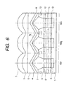
- Fig. 6 is a sectional view of an image pickup element.
- reference numeral 1 denotes a silicon wafer; 2, a microlens; 3, a photoelectric conversion section having a function for converting a received photon into an electric charge; 4 (4r and 4g), dichroic films serving as a wavelength selection section for separating wavelengths of a light; 6, a first refractive index area having a first refractive index; 5, a second refractive index area having a second refractive index; 8, a third refractive index area having a third refractive index; 9, a fourth refractive index area having a fourth refractive index; 7, a fifth refractive index area having a fifth refractive index; and 10, a Poly wiring layer serving as a gate for controlling an electric charge of the photoelectric conversion section.
- Reference numerals 11 to 13 denote wiring layers made of a metal such as aluminum.
- reference numeral 11 denotes an AL1 wiring layer serving as a connection between respective sections and an output line; 12, an AL2 wiring layer serving as a well power supply line and a control line; and 13, an AL3 wiring layer serving as a light shield and a power supply line.
- Fig. 7 schematically shows only nine pixels extracted out of a large number of pixels in the form of a perspective view of the image pickup element viewed obliquely from above.
- Fig. 8 shows a sectional view cut along the structures from microlens 2 to the AL3 wiring layer through the dichroic film 4 in the central part of Fig. 7.
- the microlens 2 is formed in an upwardly convex spherical shape and has a positive lens power. Therefore, the microlens 2 functions to condense light which has reached on the microlens 2 to the photoelectric conversion section 3. Consequently, since more light beams can be taken into the photoelectric conversion section 3, it becomes possible to increase a sensitivity of the image pickup element.
- the second refractive index area 5 adjacent to the microlens 2 plays an extremely important optical role in this structure in combination with the first refractive index area 6.
- the second refractive index area is formed of a material with a low refractive index. For example, magnesium fluoride (MgF 2 ) with a refractive index of 1.38 or the like can be used as the material.
- the first refractive index area 6 sandwiched between the second refractive index area 5 and the dichroic film 4 is formed of a material with a high refractive index.
- a material with a high refractive index for example, titanium dioxide (TiO 2 ) with a refractive index of 2.5 or the like can be used as the material.
- the third refractive index area 8, the fourth refractive index area 9, and the fifth refractive index area 7 form a second important optical element in this structure.
- the first refractive index area 8 is formed of a material with a high refractive index such as titanium dioxide and the fourth refractive index area 9 is formed of a material with a low refractive index such as silicon dioxide (SiO 2 ) or magnesium fluoride having a refractive index of 1.46. Consequently, since light incident on the third refractive index area 8 tends to be totally reflected on an interface between the third refractive index area 8 and the fourth refractive index area 9, these areas play a role of a light guide path leading to the photoelectric conversion section 3.
- the fifth refractive index area 7 it is necessary to form the fifth refractive index area 7 using a material having a refractive index equal to or lower than that of the third refractive index area 8 such that light is not totally reflected on an interface between the fifth refractive index area 7 and the third refractive index area 8.
- a difference of refractive indexes between the first refractive index area 6 and the fifth refractive index area 7 is desirably not too large, for example, silicon nitride (Si 3 N 4 ) with a refractive index of 2.0 or the like can be used.
- a dichroic film is formed by alternately stacking a substance with a high refractive index and a substance with a low refractive index with a film thickness which is an integer times of 1/4 of a wavelength ⁇ of interest.
- a wavelength of a transmitted beam can be selected.
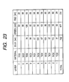
- Fig. 23 shows an example of the dichroic film 4 used in this embodiment. Titanium dioxide and silicon dioxide is used as a material with a high refractive index and a material with a low refractive index, respectively, and film thickness and the number of layers are set as shown in the table. Transmission characteristics of the dichroic film 4 are shown in Fig. 24. As it is seen from a characteristic graph of Fig.
- the dichroic film 4 has characteristics which are close to characteristics shown in the characteristic graph of color filters using the conventional dyes shown in Fig. 3. Therefore, even an image pickup element using the dichroic film 4 with this structure can have characteristics close to characteristics of the conventional image pickup element.
- These stacked films can be produced easily by using Physical Vapor Deposition (PVD).
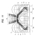
- Fig. 11 shows behaviors of only light which is incident on a pixel 100g for receiving green light and reflected by a dichroic film 4g, that is, light including blue light and red light.
- the object light 110 coming from above in the figure is incident on a microlens 2 and subjected to a condensing action.
- the light is incident on a second refractive index area 5 and a first refractive index area 6 in order and reach the dichroic film 4g.
- light other than green light is subjected to a reflecting action due to characteristics of the dichroic film 4g. Consequently, the light travels to a direction of the second refractive index area 5.
- the dichroic film 4g is formed on a surface having a square pyramid shape as shown in Fig. 9, the reflected light changes a direction from a center to an outside thereof and travel.
- the first refractive index area 6 has a higher refractive index than the second refractive index area 5
- light having an angle equal to or larger than a critical angle is subjected to a total reflection action on the interface between the first refractive index area 6 and the second refractive index area 5.
- the light totally reflected on the interface is directed to a direction of a dichroic film 4r and travels toward pixels 100r and 101r for receiving red light which are adjacent pixels.
- the dichroic film 4r of the pixels 100r and 101r has a characteristic for transmitting red light and reflecting green light and blue light. Therefore, only red light among the light reflected from the pixel 100g is transmitted and blue light is subjected to a reflecting action by the dichroic film 4r.
- the blue light subjected to the reflecting action is not illustrated because the blue light travels to the outside of the image pickup element.
- the dichroic film 4r that transmits reflected light an area in which light can be transmitted is reduced by an amount equivalent to a film thickness.
- an area of light incident on the dichroic film 4g according to a condensing action of the microlens 2 (area of reflected light) is small compared with an opening area of the microlens 2. Therefore, eclipse of the reflected light on the dichroic film 4r can be reduced.
- the light transmitted through the dichroic film 4r travels through a fifth refractive index area 7 and a third refractive index area 8 in order.
- this interface is formed of two surfaces which are substantially parallel in the vertical direction, the light, which has not been incident on the photoelectric conversion section 3 by the first total reflection, is totally reflected again on an interface on the opposite side, and all the light are finally incident on the photoelectric conversion section 3.
- a pixel for receiving blue light exists in a vertical direction with respect to the paper surface. As in the case of a red light, the pixel exhibits a behavior of taking in only the blue light among light reflected by the pixel 100g.
- Fig. 12 shows behaviors of light subjected to a transmitting action in the dichroic film 4.
- Light coming from above in this figure is incident on the microlens 2 and is subjected to a condensing action. Next, the light is incident on the second refractive index area 5 and the first refractive index area 6 in order and reaches the dichroic film 4g. Only light with a predetermined wavelength is selectively transmitted through the dichroic film 4g and is incident on the fifth refractive index area 7.
- the third refractive index area 8 makes it possible to take in light of a wide area.
- the interface between the third refractive index area 8 and the fourth refractive index area 9 is formed in a taper shape with a widened incident portion, the interface can take in light of a wide area.
- the light is subjected to an action for repeating total reflection on the interface between the third refractive index area 8 and the fourth refractive index area 9, thereby being guided to the photoelectric conversion section 3. It is seen from this that, even if light is transmitted, the light of a sufficiently wide area can be taken in.
- Fig. 25 shows a simplified transmission characteristic of each color in the dichroic film.
- the reverse of a transmission curve of each color indicates a reflection characteristic.
- a pixel array is in a form of the Bayer array as shown in Fig. 13.
- Fig. 26 shows characteristics in this case.
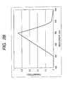
- characteristics of light reaching a red pixel from the green pixel are shown in Fig. 27, characteristic of light reaching the green pixel from the red pixel are shown in Fig. 28, and characteristics of light reaching the green pixel from the blue pixel are shown in Fig. 29.
- an amount of light which the green pixel receives from the adjacent pixels is ⁇ (light reflected by the blue pixels) ⁇ 1/4 ⁇ 2 + (light reflected by the red pixels) ⁇ 1/4 ⁇ 2 ⁇ . Since an amount of light which the green pixel receives originally is an integrated amount of a transmittance curve, when this is assumed to be one, an integrated amount in Fig. 28 (light reflected by the red pixel) is 0.74, and an integrated amount in Fig. 29 (light reflected by the blue pixel) is 0.85. Therefore, since a total amount of reflected light is 0.80, it is seen that an amount of light which the blue pixel receives is 1.80 times as large as that in the case in which only transmitted light is taken in.
- the blue pixel there are four blue pixels as adjacent pixels.
- an integrated amount of a transmittance curve of the blue pixel is one
- an integrated amount in Fig. 26 is 0.84. Since an amount of light which the blue pixel receives from the adjacent pixels is ⁇ (light reflected by the green pixels) ⁇ 1/4 ⁇ 4 ⁇ , it is seen that a total amount of reflected light is 0.84, which is 1.84 times as large as the original transmitted amount.
- red pixel there are four green pixels as adjacent pixels as in the case of the blue pixel.
- an integrated amount of a transmittance curve of the red pixel is one
- an integrated amount in Fig. 27 is 0.67. Since an amount of light which the red pixel receives from the adjacent pixels is ⁇ (light reflected by the green pixels) ⁇ 1/4 ⁇ 4 ⁇ , it is seen that a total amount of reflected light is 0.67, which is 1.67 times as large as the original transmitted amount.
- an unnecessary wavelength component is divided and reflected to the adjacent pixels, whereby the unnecessary wavelength component can be photoelectrically converted into an effective wavelength component in the adjacent pixels, and it is possible to significantly increase the efficiency of utilization of light.
- a substantial light receiving opening is larger than each pixel.
- the conventional opening of a G pixel is a size of a microlens
- a pixel opening is larger than the original pixel opening 91 because it receives portions of 92a, 92b, 92c, and 92d from adjacent pixels as shown in Fig. 14.
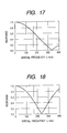
- Figs. 16 to 22 are graphs explaining the above.
- Fig. 16 shows an MTF with respect to a spatial frequency component in a horizontal direction for a pixel 110g of the image pickup element according to this embodiment.
- Fig. 17 shows an MTF of a pixel having a normal rectangular opening. It is assumed that a size of one pixel is ⁇ 3 ⁇ m and a microlens has a size equivalent to one pixel in both the cases. Moreover, it is assumed that the pixel of this embodiment has an opening extending to a central part of an adjacent pixel.
- a response of a conventional pixel having a rectangular opening can be briefly expressed by a SINC function such as expression (2) below.
- R 3 ( u ) sin( ⁇ d ⁇ u ) ( ⁇ d ⁇ u )
- R3(u) is a response and d is a width of a light receiving opening of an image pickup element.
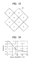
- a response increases to a high frequency side due to a diamond-shaped opening as shown in Fig. 15. It is sufficient to consider that this is a collection of limitlessly thin strip-like rectangular openings whose MTF can be expressed by expression (2). A result of integrating the entire thin strip-like rectangular opening is as shown in Fig. 16. It is seen that, at a Nyquist frequency of 167/mm in case that a pixel pitch is assumed to be 3 ⁇ m, the pixel 100g has a rather lower response.
- Fig. 19 shows an MTF of an aplanatic lens in case that an F number is assumed to be 4.0 and a wavelength of an object image is assumed to be 550 nm.
- an MTF thereof depends upon diffraction of light.
- a diffraction limit MTF depends upon the F number and is expressed by expression (3) below.
- u is a spatial frequency of an optical image
- F is an F number of an optical system
- ⁇ is a wavelength of the optical image
- a cut-off frequency of this imaging lens is 455/mm.
- Fig. 20 shows a total MTF of an imaging lens and pixels of an image pickup element in case that the pixel 100g is used.
- Fig. 21 shows a total MTF of an imaging lens, an optical lowpass filter, and pixels of an image pickup element in case that the conventional pixel is used. Both the pixels have substantially equal responses at the Nyquist frequency of 167/mm and exhibits very similar characteristics as a whole.
- the optical lowpass filter is not used in the conventional pixel, a response becomes too high at a Nyquist frequency as shown in Fig. 22. In this way, it is seen that the optical lowpass filter can be eliminated if the pixel 100g is used.
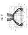
- Fig. 30 shows a second embodiment of the present invention. It is assumed that components denoted by the identical reference symbols perform the identical functions. Behaviors of light in an image pickup element in this embodiment are as shown in Figs. 31 and 32. As in the first embodiment, Fig. 31 shows behaviors of only light which is incident on a pixel 200g for receiving green light and reflected by the dichroic film 4g, that is, light including blue light and red light. Light which has exited a pupil of an imaging lens placed in a sufficiently distant position compared with a size of a pixel, passes through an infrared light cut filter to become light beams like object light 120. The object light 120 coming from above in the figure is incident on the microlens 2 and subjected to a condensing action.
- the light is incident on the second refractive index area 5 and the first refractive index area 6 in order and reach the dichroic film 4g.
- light other than green light is subjected to a reflecting action due to characteristics of the dichroic film 4g.
- the dichroic film 4g is formed on a surface having a square pyramid shape as shown in Fig. 9, the reflected light changes a direction to an outer side than a center thereof and travels.
- light having an angle equal to or larger than a critical angle is subjected to a total reflection action on the interface between the first refractive index area 6 and the second refractive index area 5.
- the light directed downward again travels toward pixels 200r and 201r for receiving red light which is adjacent pixels.
- the light transmitted through the dichroic film 4r travel through the fifth refractive index area 7 and the third refractive index area 8 in order.
- the light travels to the third refractive index area 8 since its shape is a square pyramid in the first embodiment, the light is incident on a surface thereof at an angle close to a right angle with respect to the surface.
- the third refractive index area 8 is formed as a flat surface, an incident angle is reduced and an action for largely curving the light to the central direction is applied to the light.
- more light can be totally reflected on the interface between the third refractive index area 8 and the fourth refractive index area 9 compared with the first embodiment.
- the light repeats the total reflection on the interface between these areas, thereby reaching the photoelectric conversion section 3.
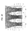
- Fig. 32 shows behaviors of light subjected to a transmitting action in the dichroic film 4.
- Light coming from above in this figure is incident on the microlens 2 and is subjected to a condensing action.
- the light is incident on the second refractive index area 5 and the first refractive index area 6 in order and reach the dichroic film 4g.
- Only light with a predetermined wavelength is selectively transmitted through the dichroic film 4 and is incident on the fifth refractive index area 7.
- the light is subjected to an action for repeating total reflection on the interface between the third refractive index area 8 and the fourth refractive index area 9, thereby being guided to the photoelectric conversion section 3. It is seen from this that, even if light is transmitted, the light of a sufficiently wide area can be taken in.
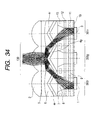
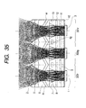
- Fig. 33 shows a third embodiment of the present invention. It is assumed that components denoted by the identical reference symbols perform the identical functions. Behaviors of light in an image pickup element in this embodiment are as shown in Figs. 34 and 35. As in the first embodiment, Fig. 34 shows behaviors of only light which is incident on the pixel 100g for receiving green light and reflected by the dichroic film 4g, that is, light including blue light and red light. Light which has exited a pupil of an imaging lens placed in a sufficiently distant position compared with a size of a pixel, passes through an infrared light cut filter to become light beams like object light 130. The object light 130 coming from above in the figure is incident on the microlens 2 and subjected to a condensing action.
- the light is incident on the second refractive index area 5 and the first refractive index area 6 in order and reach the dichroic film 4g.
- light other than green light is subjected to a reflecting action due to characteristics of the dichroic film 4g. Since the dichroic film 4g is formed on a surface of a square pyramid shape as shown in Fig. 9, the reflected light changes a direction from a center to an outside thereof and travels. Then, light having an angle equal to or larger than a critical angle is subjected to a total reflection action on the interface between the first refractive index area 6 and the second refractive index area 5.
- the interface between the second refractive index area 5 and the first refractive index area 6 has an upwardly convex spherical shape, the interface serves as a concave mirror and performs a function for condensing light. Consequently, since light beams can be collected, it becomes possible to take in light of a wide area. Subsequent behaviors of the light until it reach the photoelectric conversion section 3 are the same as those in the second embodiment.
- Fig. 35 shows behaviors of light subjected to a transmitting action in the dichroic film 4g. Behaviors of the light coming from above in the figure until it reaches the photoelectric conversion section 3 are the same as those in the second embodiment. As it is evident from this figure, transmitted light in a substantially wide area can also be taken in.
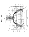
- Fig. 36 shows a fourth embodiment of the present invention. It is assumed that components denoted by the identical reference symbols perform the identical functions. In this embodiment, it is more desirable to use a material with a low refractive index such as magnesium fluoride or silicon dioxide in the microlens 2 because it is necessary that light tends to be totally reflected on the interface between the microlens 2 and the first refractive index area 6. Behaviors of light in an image pickup element in this embodiment are as shown in Figs. 37 and 38. As in the first embodiment, Fig. 37 shows behaviors of only light which is incident on the pixel 100g for receiving green light and reflected by the dichroic film 4g, that is, light including blue light and red light.
- a material with a low refractive index such as magnesium fluoride or silicon dioxide
- the object light 140 coming from above in the figure is incident on the microlens 2 and subjected to a condensing action.
- the light reaches the dichroic film 4g through the first refractive index area 6. Subsequent behaviors of the light until it reaches the photoelectric conversion section 3 are the same as those in the second embodiment.
- Fig. 38 shows behaviors of light subjected to a transmitting action in the dichroic film 4.
- the light coming from above in the figure is incident on the microlens 2 and subject to a condensing action.
- the light reaches the dichroic film 4g through the first refractive index area 6.
- behaviors of the light until it reaches the photoelectric conversion section 3 are the same as those in the second embodiment.
- transmitted light in a sufficiently wide area can also be taken in.
- Figs. 39 to 60 show a fifth embodiment of the present invention.
- Fig. 39 is a sectional view of an image pickup element.
- reference numeral 201 denotes a silicon wafer; 202, a microlens; 203, a photoelectric conversion section having a function for converting a received photon into an electric charge; 204 (204r and 204g), dichroic films serving as a wavelength selection section for separating wavelengths of a light; 205, a third refractive index area having a third refractive index; 206, a fourth refractive index area having a fourth refractive index; 207, a fifth refractive index area having a fifth refractive index; 208, a first refractive index area having a first refractive index; 209, a second refractive index area having a second refractive index; and 210, a Poly wiring layer serving as a gate for controlling an electric charge of the photoelectric conversion section.
- Reference numerals 211 to 213 denote wiring layers made of a metal such as aluminum.
- reference numeral 211 denotes an AL1 wiring layer serving as a connection and an output line between adjacent two sections; 212, an AL2 wiring layer serving as a well power supply line and a control line; and 213, an AL3 wiring layer serving as light shield and a power supply line.
- Fig. 40 schematically shows only nine pixels extracted out of a large number of pixels in the form of a perspective view of the image pickup element viewed obliquely from above.
- Fig. 41 shows a sectional view cut along the structures from the microlens 202 to the AL3 wiring layer through the dichroic film 4 in the central part of Fig. 40.
- the microlens 202 is formed in an upwardly convex spherical shape and has a positive lens power. Therefore, the microlens 202 functions to condense light which have reached on the microlens 202 to the photoelectric conversion section 203. Consequently, since more light beams can be taken into the photoelectric conversion section 203, it becomes possible to increase a sensitivity of the image pickup element.
- the third refractive index area 205 is formed of a material with a low refractive index. For example, magnesium fluoride (MgF 2 ) with a refractive index of 1.38 or the like can be used as the material.
- the fourth refractive index area 6 sandwiched by the third refractive index area 205 and the dichroic film 204 is formed of a material with a high refractive index.
- a material with a high refractive index for example, titanium dioxide (TiO 2 ) with a refractive index of 2.5 or the like can be used as the material.
- the first refractive index area 208 is formed of a material with a high refractive index such as titanium dioxide and the second refractive index area 209 is formed of a material with a low refractive index such as silicon dioxide (SiO 2 ) or magnesium fluoride having a refractive index of 1.46. Consequently, since light incident on the first refractive index area tends to be totally reflected on an interface between the first refractive index area and the second refractive index area, these areas play a role of a light guide path leading to the photoelectric conversion section 203.
- the fifth refractive index area 207 it is necessary to form the fifth refractive index area 207 using a material having a refractive index equal to or lower than that of the first refractive index area such that light is not totally reflected on an interface between the fifth refractive index area and the first refractive index area.
- a difference of refractive indexes between the second refractive index area 206 and the fifth refractive index area 207 is desirably not too large, for example, silicon nitride (Si 3 N 4 ) with a refractive index of 2.0 or the like can be used.
- a dichroic film is formed by alternately stacking a material with a high refractive index and a material with a low refractive index with a film thickness which is an integer times of 1/4 of a wavelength ⁇ of interest.
- a wavelength of a transmitted beam can be selected.
- Fig. 55 shows an example of the dichroic film 204 used in this embodiment. Titanium dioxide and silicon dioxide is used as a material with a high refractive index and a material with a low refractive index, respectively, and the film thickness and the number of layers are set as shown in the table. Transmission characteristics of the dichroic film 4 are shown in Fig. 56. As it is seen from a characteristic graph of Fig.
- the dichroic film 204 has characteristics which are close to characteristics shown in the characteristic graph of color filters using the conventional pixels shown in Fig. 3. Therefore, even an image pickup element using the dichroic film 204 with this structure can have characteristics close to characteristics of the conventional image pickup element.
- These stacked films can be produced easily by using Physical Vapor Deposition (PVD).
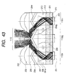
- Fig. 43 shows behaviors of only light which is incident on a pixel 1100g for receiving green light and reflected by a dichroic film 204g, that is, light including blue light and red light.
- the object light 1100 coming from above in the figure is incident on a microlens 202 and subjected to a condensing action.
- the light is incident on a third refractive index area 205 and a fourth refractive index area 206 in order and reach the dichroic film 204g.
- light other than green light is subjected to a reflecting action due to characteristics of the dichroic film 204g. Consequently, the light travels to a direction of the third refractive index area 205.
- the dichroic film 204g is formed on a surface having a square pyramid shape as shown in Fig. 42, the reflected light changes a direction from a center to an outside thereof and travels.
- the fourth refractive index area 206 has a higher refractive index than the third refractive index area 205, light having an angle equal to or larger than a critical angle are subjected to a total reflection action on the interface between the fourth refractive index area 206 and the third refractive index area 205.
- the light totally reflected on the interface is directed to a direction of a dichroic film 204r and travels toward pixels 1100r and 1101r for receiving red light which are adjacent pixels.
- the dichroic film 204r of the pixels 1100r and 1101r has a characteristic for transmitting red light and reflecting green light and blue light.
- the light transmitted through the dichroic film 204r travels through a fifth refractive index area 207 and a first refractive index area 208 in order. Subsequently, the light is about to travel from the first refractive index area 208 to the second refractive index area 209. Again, as described above, since the first refractive index area 208 has a higher refractive index than the second refractive index area 209, light having an angle equal to or lager than a critical angle is totally reflected on a surface between the first refractive index area 208 and the second refractive index area 209.
- the interface between the first refractive index area 208 and the second refractive index area 209 is formed in a taper shape with a widened incident portion, a frontage for taking in incident light is widened and a large amount of light can be taken in the first refractive index area 208. If the incident portion of the first refractive index area 208 is not formed in a taper shape, light located on a lower side in the figure among the reflected light travels from the fifth refractive index area 207 to the second refractive index area 209. Then, since the fifth refractive index area 207 has a higher refractive index than the second refractive index area 209, the light is curved upward. Next, the light travel to the first refractive index area 208.
- the first refractive index area 208 has a higher refractive index than the second refractive index area 209, the light is curved upward further. Therefore, since the light following such a route is not guided to the photoelectric conversion section 203 but lost, reflected light from the adjacent pixels can be sufficiently taken in by forming the first the first refractive index area 208 in a taper shape to eliminate light traveling from the fifth refractive index area 207 to the second refractive index area 209.
- the interface between the first refractive index area 208 and the second refractive index area 209 is formed of two surfaces which are substantially parallel with an optical axis of an imaging lens, the light, which has not been incident on the photoelectric conversion section 203 by the first total reflection, is totally reflected again on an interface on the opposite side and is finally incident on the photoelectric conversion section 203.
- a pixel for receiving blue light exists in a vertical direction with respect to the paper surface. As in the case of a red light, the pixel exhibits a behavior of taking in only the blue light among light reflected by the pixel 1100g.
- Fig. 44 shows behaviors of light subjected to a transmitting action in a dichroic film 204.
- the light coming from above in the figure is incident on the microlens 202 and subject to a condensing action. Next, the light is incident on the third refractive index area 205 and the fourth refractive index area 206 in order and reach the dichroic film 204g. Only light with a predetermined wavelength is selectively transmitted through the dichroic film 204g and is incident on the fifth refractive index area 207.
- the light travels to the first refractive index area 208 and is subjected to an action for repeating total reflection on the interface between the first refractive index area 208 and the second refractive index area 209, thereby being guided to the photoelectric conversion section 203.
- the interface between the first refractive index area 208 and the second refractive index area 209 is formed in a taper shape with a widened incident portion. If a taper surface 281a on which the taper shape is formed has a too sharp angle, light may not be totally reflected on the taper surface 281a, or even if the light is totally reflected, the light is not then totally reflected on a surface on the opposite side but transmitted.
- the light is totally reflected on the taper surface 281a and can be guided to the photoelectric conversion section 3.
- the taper surface 281a By setting the taper surface 281a to an appropriate angle and using it, it becomes possible to take in light of a wide area.
- Fig. 3 shows a spectral transmittance characteristic of R, G, and B color filters in an image pickup element. Since a transmittance of infrared light is high, an infrared light cut filter for blocking a wavelength of 650 nm or more is actually further laid over these color filters between the image pickup element and an image pickup lens. As it is seen from this, only approximately one third of visible light is used effectively in one pixel.
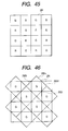
- an area ratio of R, G, and B pixels of a color image pickup element of the Bayer array shown in Fig. 45 is 1/4 : 2/4 : 1/4 in case that an area of one unit constituting a regular array is assumed to be one.
- Fig. 57 shows a simplified transmission characteristic of each color in the dichroic film.
- the reverse of a transmission curve of each color indicates a reflection characteristic.
- a pixel array is in a form of the Bayer array as shown in Fig. 45.
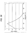
- Fig. 58 shows characteristics in this case.
- characteristics of light reaching a red pixel from the green pixel are shown in Fig. 59
- characteristic of light reaching the green pixel from the red pixel are shown in Fig. 60
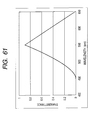
- characteristics of light reaching the green pixel from the blue pixel are shown in Fig. 61.
- an amount of light which the green pixel receives from the adjacent pixels is ⁇ (light reflected by the blue pixels) ⁇ 1/4 ⁇ 2 + (light reflected by the red pixels) ⁇ 1/4 ⁇ 2 ⁇ . Since an amount of light which the green pixel receives originally is an integrated amount of a transmittance curve, in case that this is assumed to be one, an integrated amount in Fig. 60 (light reflected by the red pixel) is 0.74, and an integrated amount in Fig. 61 (light reflected by the blue pixel) is 0.85. Therefore, since a total amount of reflected light is 0.80, it is seen that an amount of light which the blue pixel receives is 1.80 times as large as that in the case in which only transmitted light is taken in.
- the blue pixel there are four green pixels as adjacent pixels.
- an integrated amount of a transmittance curve of the blue pixel is one
- an integrated amount in Fig. 58 is 0.84. Since an amount of light which the blue pixel receives from the adjacent pixels is ⁇ (light reflected by the green pixels) ⁇ 1/4 ⁇ 4 ⁇ , it is seen that a total amount of reflected light is 0.84, which is 1.84 times as large as the original transmitted amount.
- red pixel there are four green pixels as adjacent pixels as in the case of the blue pixel.
- an integrated amount of a transmittance curve of the red pixel is one
- an integrated amount in Fig. 59 is 0.67. Since light which the red pixel receives from the adjacent pixels is ⁇ (light reflected by the green pixels) ⁇ 1/4 ⁇ 4 ⁇ , it is seen that a total amount of reflected light is 0.67, which is 1.67 times as large as an original transmitted amount.
- an unnecessary wavelength component is divided and reflected to the adjacent pixels by using the present structure, whereby the unnecessary wavelength component can be photoelectrically converted into an effective wavelength component in the adjacent pixels, and it is possible to significantly increase the efficiency of utilization of light.
- image pickup for obtaining satisfactory image characteristics consists of a first process for forming an object image with an optical apparatus, a second process for adjusting a high frequency component of a spatial frequency characteristic of the object image such that the high frequency component is suppressed, a third process for photoelectrically converting the object image whose spatial frequency characteristic has been adjusted, and a fourth process for correcting a response according to a spatial frequency with respect to an obtained electric signal.
- the Nyquist frequency is a frequency which is a half of a sampling frequency depending upon a pixel pitch. Therefore, the optimized series of processes can obtain a high quality image, in which aliasing distortion is less conspicuous, that is, moiré is less conspicuous, by adjusting an optical image to be sampled so as to be an optical image of a characteristic according to the Nyquist frequency peculiar to the image pickup element.
- a Modulation Transfer Function which is a spatial frequency transmission characteristic of an image, is an evaluation amount with which a characteristic concerning a sharpness of a digital still camera, a video camera, or the like can be represented well.
- Specific factors affecting this MTF are an imaging optical system serving as an optical apparatus, an optical lowpass filter for band limitation of an object image, an opening shape of a photoelectric conversion area of an image pickup element, digital aperture correction, and the like.
- An overall MTF representing a final image characteristic is given as a product of MFTs of the respective elements. That is, it is sufficient to find MTFs of the above-mentioned first to fourth processes and calculate a product of the MTFs.
- the structure for reducing a component having a frequency more than the Nyquist frequency peculiar to the image pickup element in the spatial frequency characteristic of the optical image means that a component having a frequency more than the Nyquist frequency is small in the product of MTFs of the first, second, and third processes excluding the fourth process.
- image pickup is performed on the premise that a still image is viewed as in a digital still camera, it is necessary to take into account the fact that an image tends to appear as an image with a higher resolution if a response in a frequency slightly below the Nyquist frequency is higher even if high frequencies exceeding the Nyquist frequency are not eliminated but remain more or less.
- an optical aberration can be corrected easier in a center of a screen than in a peripheral part of the screen. It is necessary to obtain an extremely satisfactory characteristic close to a diffraction limit MTF, which depends upon an F number of an imaging lens, in the center of the image in order to obtain a satisfactory image in the peripheral part of the screen. In recent year, since miniaturization of pixels of an image pickup element has been advanced, this necessity is increasing. Therefore, it is better to consider the MTF for an imaging optical system assuming that the imaging optical system is an ideal aplanatic lens.
- an optical lowpass filter is usually used.
- a material having a birefringent characteristic such as a rock crystal is utilized for the optical lowpass filter.
- a phase-type diffraction grating may be utilized.
- R2(u) is a response
- u is a spatial frequency of an optical image
- ⁇ is an object image separation width
- the same effect can be obtained by separating the optical image into a plurality of images having a predetermined positional relationship and superimposing the images in accordance with diffraction.
- a substantial light receiving opening is larger than each pixel.
- the conventional opening of a G pixel is a size of a microlens
- a pixel opening is larger than the original pixel opening 291 because it receives portions of 292a, 292b, 292c, and 292d from adjacent pixels as shown in Fig. 46. Consequently, a substantial light receiving opening including the sparing of green light component by the adjacent pixels is as shown in Fig. 47.
- the B pixel and the R pixel also have each color light component spared by the adjacent pixels, effective light receiving openings for these pixels have the similar shape to the G pixel. Therefore, as to all the pixels, it is seen that the pixels have light receiving openings which overlap with each other effectively.
- Fig. 48 shows an MTF with respect to a spatial frequency component in a horizontal direction for a pixel 1110g of the image pickup element according to this embodiment.
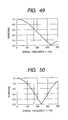
- Fig. 49 shows an MTF of a pixel having a normal rectangular opening. It is assumed that a size of one pixel is ⁇ 3 ⁇ m and a microlens has a size equivalent to one pixel in both the cases. Moreover, it is assumed that the pixel of this embodiment has an opening extending to a central part of an adjacent pixel.
- a response of a conventional pixel having a rectangular opening shown in Fig. 45 can be briefly expressed by a SINC function such as expression (2) below.
- R 3 ( u ) sin( ⁇ d ⁇ u ) ( ⁇ d ⁇ u )
- R3(u) is a response and d is a width of a light receiving opening of an image pickup element.
- a response increases to a high frequency side due to a diamond-shaped opening as shown in Fig. 47. It is sufficient to consider that this is a limitless collection of limitlessly thin strip-like rectangular openings whose MTF can be expressed by expression (2).
- a result of integrating the entire thin strip-like rectangular opening is as shown in Fig. 48. It is seen that, in a Nyquist frequency of 167/mm in case that a pixel pitch is assumed to be 3 ⁇ m, the pixel 100g has a rather lower response.
- Fig. 51 shows an MTF of an aplanatic lens in case that an F number is assumed to be 4.0 and a wavelength of an object image is assumed to be 550 nm.
- an MTF thereof depends upon diffraction of light.
- a diffraction limit MTF depends upon the F number and is expressed by expression (3) below.
- u is a spatial frequency of an optical image
- F is an F number of an optical system
- ⁇ is a wavelength of the optical image
- a cut-off frequency of this imaging lens is 455/mm.
- Fig. 52 shows a total MTF of an imaging lens and pixels of an image pickup element in case that the pixel 1100g is used.
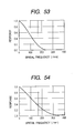
- Fig. 53 shows a total MTF of an imaging lens, an optical lowpass filter, and pixels of an image pickup element in case that the conventional pixel is used. Both the pixels have substantially equal responses at the Nyquist frequency of 167/mm and exhibits very similar characteristics as a whole.
- the optical lowpass filter is not used in the conventional pixel, a response becomes too high at a Nyquist frequency as shown in Fig. 54. In this way, it is seen that the optical lowpass filter can be eliminated if the pixel 1100g is used.
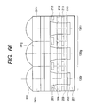
- the image pickup element may include color filters as shown in Fig. 66, which transmit light of a specific wavelength range and absorb light of other wavelength ranges, as a wavelength transmission section instead of the dichroic films as shown in Fig. 39.
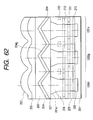
- Fig. 62 shows a sixth embodiment of the present invention. It is assumed that components denoted by the identical reference symbols as those in Fig. 39 perform the identical functions. Behaviors of light in an image pickup element in this embodiment are as shown in Figs. 63 and 64.
- An image pickup element shown in Fig. 63 is an image pickup element which is located in a place spaced apart from an optical axis of an imaging lens. Since the optical axis is on a right side of this figure, a pupil center of the imaging lens is located in the right side and light incident on the microlens 202 has an angle leaning to a right direction.
- the microlens 202 is arranged to be inclined to a right side from a center of a pixel, whereby more obliquely incident light can be taken in.
- Fig. 63 shows behaviors of only light which is incident on a pixel 1200g for receiving green light and reflected by the dichroic film 204g, that is, light including blue light and red light.
- the object light 1120 coming from above in the figure is incident on the microlens 202 and subjected to a condensing action.
- the light is incident on the third refractive index area 205 and the fourth refractive index area 206 in order and reach the dichroic film 204g.
- light other than green light is subjected to a reflecting action due to characteristics of the dichroic film 204g.
- the dichroic film 204g is formed on a surface having a square pyramid shape as shown in Fig. 42, the reflected light changes a direction from a center to an outside thereof and travels.
- a vertex of the square pyramid forming the dichroic film 204g is formed in a shape inclined to the right side.
- angles of slopes are different.
- angles of light incident on a right side slope and a left side slope of the dichroic film 204g, respectively, can be matched.
- light having an angle equal to or larger than a critical angle is subjected to a total reflection action on the interface between the fourth refractive index area 206 and the third refractive index area 205.
- the light directed downward again travels toward pixels 1200r and 1201r for receiving red light which are adjacent pixels.
- the light transmitted through the dichroic film 204r travels through the fifth refractive index area 207 and the first refractive index area 208 in order. Subsequently, the light is about to travel from the first refractive index area 208 to the second refractive index area 209.
- the first refractive index area 208 has a higher refractive index than the second refractive index area 209 as described above, light incident at an angle equal to or larger than a critical angle is totally reflected on the interface. Since the interface between the first refractive index area 208 and the second refractive index area 209 is formed in a taper shape with a widened incident portion, a frontage for taking in incident light is widened and a large amount of light can be taken in the first refractive index area 208.
- the interface in the vicinity of the photoelectric conversion section 203 is formed of two surfaces which are substantially parallel with an optical axis of an imaging lens, the light, which has not been incident on the photoelectric conversion section 203 by the first total reflection, is totally reflected on an interface on the opposite side again and all the light are finally incident on the photoelectric conversion section 203.
- Fig. 64 shows behaviors of light which are subjected to a transmitting action in the dichroic film 204.
- light coming from above in this figure is incident on the microlens 202 and is subjected to a collimating action.
- the light is incident on the third refractive index area 205 and the fourth refractive index area 206 in order and reach the dichroic film 204g. Only light with a predetermined wavelength is selectively transmitted through the dichroic film 204g and is incident on the fifth refractive index area 207.
- the light travels to the first refractive index area 208 and is subjected to an action for repeating total reflection on the interface between the first refractive index area 208 and the second refractive index area 209, thereby being guided to the photoelectric conversion section 203.
- the interface between the first refractive index area 208 and the second refractive index area 209 is formed in a taper shape with a widened incident portion, the light can be also totally reflected on the taper surface 281a and guided to the photoelectric conversion section 203. If this taper surface 281a is formed in the same shape as pixels in the vicinity of an optical axis center of an imaging lens as shown in Fig.
- the light totally reflected on the taper surface 281a cannot be totally reflected on a surface on the opposite side and passes through to the second refractive index area 209.
- an angle defined between the optical axis and the taper surface is made smaller than that in the vicinity of the center, whereby an angle of the light reflected on the taper surface does not exceed a critical angle on the surface on the opposite side and light of a sufficiently wide area can be taken in as in the pixels in the vicinity of the center.
- angles of taper surfaces are made symmetrical with respect to a central axis of a pixel.
- light totally reflected on a slope on a right side can be taken in both sides around the central axis. Therefore, the angles of the taper surface are not always required to be made symmetrical and a different angle may be given to each taper surface forming a taper section.
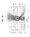
- Figs. 66 and 67 show a seventh embodiment of the present invention. It is assumed that components denoted by the identical reference symbols as those in Fig. 39 perform the identical functions.
- Fig. 66 shows pixels in the vicinity of an optical axis center of an imaging lens and
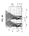
- Fig. 67 shows pixels located in a place spaced apart from the optical axis center of the imaging lens. Behaviors of light in an image pickup element in this embodiment are as shown in Figs. 68 and 69.
- the light travels to the first refractive index area 208 and is subjected to an action for repeating total reflection on the interface between the first refractive index area 208 and the second refractive index area 209, thereby being guided to the photoelectric conversion section 203. Since the interface between the first refractive index area 208 and the second refractive index area 209 is formed in a taper shape with a widened incident portion, the light can be also totally reflected on the taper surface 281a and guided to the photoelectric conversion section 203. In this embodiment, both the pixels in the vicinity of the optical axis of the imaging lens (Fig. 66) and the pixels spaced apart from the center have the same angle of the taper surface.
- an angle defined between the optical axis and the taper surface is made smaller than that in the vicinity of the center, whereby an angle of the light reflected on the taper surface does not exceed a critical angle on the surface on the opposite side and light of a sufficiently wide area can be taken in as in the pixels in the vicinity of the center.
- a solid-state image pickup element having any one of the structures of the first to seventh embodiments described above may be a charge transfer type such as a CCD solid-state image pickup element or may be an XY address type such as a CMOS image sensor.
- reference numeral 101 denotes a barrier also severs as a protect for a lens and a main switch; 102, a lens for focusing an optical image of an object on a solid-state image pickup element 104; 103, a stop for varying an amount of light having passed through the lens 102; 104, a solid-state image pickup element for taking in the optical image of the subject focused by the lens 102 as an image signal; 105, an image pickup signal processing circuit including a gain variable amplifier section for amplifying the image signal outputted from the solid-state image pickup element 104, and a gain correction circuit section for correcting a gain value; 106, an A/D converter for performing analog/digital conversion of the image signal outputted from the solid-state image pickup element; 107; a signal processing unit for applying various corrections to the image data outputted from the A/D converter 106 and compressing the data; 108, a timing generation unit for outputting various timing signals to the solid-state image pickup element 104, the image pickup signal
- a main power supply is turned on, a power supply for a control system is turned on next, and a power supply of an image pickup system circuit such as the A/D converter 106 is further turned on.
- the system control and operation unit 109 opens the stop 103, and a signal outputted from the solid-state image pickup element 104 is inputted into the signal processing unit 107 after being converted by the A/D converter 106.
- the system control and operation unit 109 performs an arithmetic operation of exposure based on data of the signal.
- the system control and operation unit 109 judges brightness from a result of performing this photometry and controls the stop 103 according to the result.
- the system control and operation unit 109 extracts a high frequency component and performs an arithmetic operation of a distance to an object based on the signal outputted from the solid-state image pickup element 104. Thereafter, the system control and operation unit 109 drives the lens 102 and judges whether or not the lens 102 is focused. When it is judged that it is not focused, the system control and operation unit 109 drives the lens 102 again to perform distance measurement.
- the image signal outputted from the solid-state image pickup element 104 is A/D converted by the A/D converter 106 and written into the memory unit 110 by the system control and operation unit 109 through the signal processing unit 107. Thereafter, the data stored in the memory unit 110 is recorded on the detachable recording medium 12 such as a semiconductor memory through the recording medium control I/F unit 111 by the control of the system control and operation unit 109.
- the data may be directly inputted in a computer or the like through the external I/F unit 113 to process an image.
Landscapes
- Solid State Image Pick-Up Elements (AREA)
- Transforming Light Signals Into Electric Signals (AREA)
- Light Receiving Elements (AREA)
- Eye Examination Apparatus (AREA)
- Fluid-Damping Devices (AREA)
- Vehicle Body Suspensions (AREA)
Abstract
Description
Although it is basically possible to create a color image if there are the same number of pixels for each of three colors, an image quality can be improved by increasing the number of green pixels having a rather high visibility.
Here, it is taken into account the fact that, in the case in which image pickup is performed on the premise that a still image is viewed as in a digital still camera, an image tends to appear as an image with a higher resolution if a response in a frequency slightly below the Nyquist frequency is higher even if high frequencies exceeding the Nyquist frequency remain more or less.
Claims (23)
- An image pickup element comprising:wherein the refractive index of said first area is higher than the refractive index of said second area.a photoelectric conversion section;a wavelength selection section formed closer to an incident side of light than said photoelectric conversion section, for transmitting light of a predetermined wavelength range;a first area having a predetermined refractive index and being formed closer to the incident side of light than said wavelength selection section; anda second area having a predetermined refractive index, and being formed closer to the incident side of light than said first area,
- An image pickup element according to claim 1, further comprising:wherein the refractive index of said third area is higher than the refractive index of said fourth area.a third area having a predetermined refractive index and being formed between said wavelength selection section and said photoelectric conversion section; anda fourth area having a predetermined refractive index and being formed in a peripheral part of said third area,
- An image pickup element according to claim 2, further comprising:wherein the refractive index of said third area is higher than the refractive index of said fifth area.a fifth area having a predetermined refractive index and being formed between said third area and said wavelength selection section,
- An image pickup element according to claim 1,
wherein said second area is a microlens for condensing light. - An image pickup element according to claim 1,
wherein a microlens for condensing light is provided on said second area. - An image pickup element according to claim 4,
wherein a surface where the microlens and said second area are in contact with each other has a curvature. - An image pickup element according to claim 5,
wherein a surface where the microlens and said second area are in contact with each other has a curvature. - An image pickup element according to claim 3,
wherein said fifth area includes a slope extending from a central part to a peripheral part thereof. - An image pickup element according to claim 3,
wherein said fifth area has a square pyramid shape. - An image pickup element according to claim 1,
wherein said wavelength selection section includes a slope extending from a central part to a peripheral part thereof. - An image pickup element according to claim 1,
wherein said wavelength selection section has a square pyramid shape. - An image pickup element according to claim 10,
wherein said wavelength selection section transmits light of a first wavelength range, and also, reflects light of a second wavelength range. - An image pickup element according to claim 11,
wherein said wavelength selection section transmits light of a first wavelength range, and also, reflects light of a second wavelength range. - An image pickup apparatus comprising:an image pickup element according to claim 1;an analog/digital conversion unit which converts a signal from said image pickup element to a digital signal; anda signal processing circuit which processes the signal from said analog/digital conversion unit.
- An image pickup element comprising:wherein an interface formed between said first area and said second area includes a first interface and a second interface which is closer to an incident side of light than the first interface, and the first interface is substantially parallel with an optical axis of an imaging lens and the second interface is a slope having a substantially uniform angle with respect to the optical axis of the imaging lens.a first area having a first refractive index and guiding light to a photoelectric conversion section; anda second area having a second refractive index lower than the first refractive index and being formed in a peripheral part of said first area,
- An image pickup element according to claim 15,
wherein an opening section formed by the second interface becomes smaller as the opening section gets closer to said photoelectric conversion section. - An image pickup element according to claim 15,
wherein an angle defined by the second interface and the optical axis varies according to an distance from the optical axis in the image pickup element. - An image pickup element according to claim 15,
wherein a length of the slope that serves as the second interface varies according to an distance from the optical axis in the image pickup element. - An image pickup element according to claim 15, further comprising:wherein said wavelength selection section including a slope extending from a central part to a peripheral part thereof.a wavelength selection section formed closer to an incident side of light than said second area, for transmitting light of a predetermined wavelength,
- An image pickup element according to claim 19,
wherein said wavelength selection section has a square pyramid shape. - An image pickup element according to claim 19,
wherein said wavelength selection section transmits light of a first wavelength range, and also, reflects light of a second wavelength range. - An image pickup element according to claim 20,
wherein said wavelength selection section transmits light of a first wavelength range, and also, reflects light of a second wavelength range. - An image pickup apparatus comprising:an image pickup element according to claim 15;an analog/digital conversion unit which converts a signal from said image pickup element to a digital signal; anda signal processing circuit which processes the signal from said analog/digital conversion unit.
Applications Claiming Priority (4)
| Application Number | Priority Date | Filing Date | Title |
|---|---|---|---|
| JP2002044645 | 2002-02-21 | ||
| JP2002044645A JP4027115B2 (en) | 2002-02-21 | 2002-02-21 | Imaging device and imaging apparatus |
| JP2002044806A JP4027116B2 (en) | 2002-02-21 | 2002-02-21 | Imaging device and imaging apparatus |
| JP2002044806 | 2002-02-21 |
Publications (3)
| Publication Number | Publication Date |
|---|---|
| EP1339225A2 true EP1339225A2 (en) | 2003-08-27 |
| EP1339225A3 EP1339225A3 (en) | 2005-07-13 |
| EP1339225B1 EP1339225B1 (en) | 2011-01-12 |
Family
ID=27667552
Family Applications (1)
| Application Number | Title | Priority Date | Filing Date |
|---|---|---|---|
| EP03003855A Expired - Lifetime EP1339225B1 (en) | 2002-02-21 | 2003-02-20 | Image pickup apparatus |
Country Status (5)
| Country | Link |
|---|---|
| US (1) | US7250973B2 (en) |
| EP (1) | EP1339225B1 (en) |
| KR (1) | KR100508068B1 (en) |
| AT (1) | ATE495548T1 (en) |
| DE (1) | DE60335685D1 (en) |
Cited By (3)
| Publication number | Priority date | Publication date | Assignee | Title |
|---|---|---|---|---|
| EP1341235A3 (en) * | 2002-02-28 | 2006-05-10 | Canon Kabushiki Kaisha | Image pickup apparatus |
| CN100416844C (en) * | 2004-05-06 | 2008-09-03 | 美格纳半导体有限会社 | CMOS image sensor with prism and manufacturing method thereof |
| FR2950196A1 (en) * | 2009-09-17 | 2011-03-18 | Commissariat Energie Atomique | 3D IMAGING DEVICE EQUIPPED WITH NANO-THREADS AND METHOD OF MANUFACTURING THE SAME |
Families Citing this family (33)
| Publication number | Priority date | Publication date | Assignee | Title |
|---|---|---|---|---|
| US7834927B2 (en) * | 2001-08-22 | 2010-11-16 | Florida Atlantic University | Apparatus and method for producing video signals |
| JP2004029554A (en) * | 2002-06-27 | 2004-01-29 | Olympus Corp | Image pickup lens unit and image pickup device |
| JP3709873B2 (en) * | 2003-02-19 | 2005-10-26 | ソニー株式会社 | Solid-state imaging device and imaging camera |
| JP2005079338A (en) * | 2003-08-29 | 2005-03-24 | Matsushita Electric Ind Co Ltd | Solid-state imaging device and manufacturing method thereof |
| JP4322166B2 (en) * | 2003-09-19 | 2009-08-26 | 富士フイルム株式会社 | Solid-state image sensor |
| JP4508619B2 (en) * | 2003-12-03 | 2010-07-21 | キヤノン株式会社 | Method for manufacturing solid-state imaging device |
| WO2005101067A1 (en) | 2004-04-13 | 2005-10-27 | Matsushita Electric Industrial Co., Ltd. | Condensing element and solid state imaging device |
| US20060057765A1 (en) * | 2004-09-13 | 2006-03-16 | Taiwan Semiconductor Manufacturing Company, Ltd. | Image sensor including multiple lenses and method of manufacture thereof |
| JP2006237315A (en) * | 2005-02-25 | 2006-09-07 | Matsushita Electric Ind Co Ltd | Solid-state imaging device |
| TWI288973B (en) * | 2005-09-27 | 2007-10-21 | Visera Technologies Co Ltd | Image sensing device and manufacture method thereof |
| JP5086535B2 (en) * | 2005-11-21 | 2012-11-28 | オリンパスメディカルシステムズ株式会社 | Two-plate imaging device |
| JP2007180156A (en) * | 2005-12-27 | 2007-07-12 | Fujifilm Corp | Solid-state image sensor |
| KR100795922B1 (en) * | 2006-07-28 | 2008-01-21 | 삼성전자주식회사 | Manufacturing Method of Image Pickup Device and Image Pickup Device |
| US20080173791A1 (en) * | 2007-01-19 | 2008-07-24 | Palum Russell J | Image sensor with three sets of microlenses |
| KR100913325B1 (en) * | 2007-11-05 | 2009-08-20 | 주식회사 동부하이텍 | Dual image sensor and its manufacturing method |
| US8237121B2 (en) * | 2008-02-07 | 2012-08-07 | Omnivision Technologies, Inc. | Alternating row infrared filter for an image sensor |
| US8384818B2 (en) * | 2008-06-18 | 2013-02-26 | Panasonic Corporation | Solid-state imaging device including arrays of optical elements and photosensitive cells |
| US8633432B2 (en) * | 2009-09-21 | 2014-01-21 | California Institute Of Technology | Reflective focusing and transmissive projection device |
| US8767216B2 (en) * | 2009-10-13 | 2014-07-01 | California Institute Of Technology | Holographically illuminated imaging devices |
| JP5538811B2 (en) * | 2009-10-21 | 2014-07-02 | キヤノン株式会社 | Solid-state image sensor |
| US8536545B2 (en) | 2010-09-09 | 2013-09-17 | California Institute Of Technology | Delayed emission detection devices and methods |
| TW201245768A (en) * | 2011-03-29 | 2012-11-16 | Sony Corp | Image pickup apparatus, image pickup device, image processing method, aperture control method, and program |
| US8902338B2 (en) * | 2011-06-06 | 2014-12-02 | Panasonic Intellectual Property Corporation Of America | Color separation filter array, solid-state imaging element, imaging device, and display device |
| JP2013012506A (en) * | 2011-06-28 | 2013-01-17 | Sony Corp | Solid state imaging device manufacturing method, solid state imaging device, electronic apparatus manufacturing method and electronic apparatus |
| US20130094807A1 (en) * | 2011-10-12 | 2013-04-18 | Avago Technologies Fiber Ip (Singapore) Pte. Ltd. | Optical coupling system for use in an optical communications module, an optical communications module that incorporates the optical coupling system, and a method |
| WO2013065226A1 (en) | 2011-10-31 | 2013-05-10 | パナソニック株式会社 | Solid-state imaging element, image capture device and signal processing method |
| WO2015005672A1 (en) * | 2013-07-09 | 2015-01-15 | Samsung Electronics Co., Ltd. | Image generating apparatus and method and non-transitory recordable medium |
| KR20150006755A (en) * | 2013-07-09 | 2015-01-19 | 삼성전자주식회사 | Image generating apparatus, image generating method and non-transitory recordable medium |
| KR102159166B1 (en) * | 2014-05-09 | 2020-09-23 | 삼성전자주식회사 | Color separation device and image sensor including the color separation device |
| KR102276434B1 (en) * | 2014-07-03 | 2021-07-09 | 삼성전자주식회사 | Image sensor including color separation element and image pickup apparatus including the image sensor |
| CN107785387B (en) * | 2017-10-25 | 2020-05-05 | 德淮半导体有限公司 | Image sensor and method for forming an image sensor |
| DE102020113591B4 (en) | 2020-05-19 | 2022-02-03 | Audi Aktiengesellschaft | Image sensor device of a camera for detecting light |
| CN117146973B (en) * | 2023-11-01 | 2023-12-26 | 长春理工大学 | Spherical aberration eliminating large area array detector, spherical aberration eliminating method and detector manufacturing method |
Family Cites Families (9)
| Publication number | Priority date | Publication date | Assignee | Title |
|---|---|---|---|---|
| JP2869280B2 (en) | 1993-01-27 | 1999-03-10 | シャープ株式会社 | Solid-state imaging device and method of manufacturing the same |
| JP3402429B2 (en) | 1996-11-22 | 2003-05-06 | ソニー株式会社 | Solid-state imaging device and method of manufacturing the same |
| JPH1168074A (en) | 1997-08-13 | 1999-03-09 | Sony Corp | Solid-state imaging device |
| JP3571909B2 (en) | 1998-03-19 | 2004-09-29 | キヤノン株式会社 | Solid-state imaging device and method of manufacturing the same |
| US6078429A (en) * | 1998-07-22 | 2000-06-20 | Foveon, Inc. | Color separating prism having violet light component in red channel |
| US6583438B1 (en) * | 1999-04-12 | 2003-06-24 | Matsushita Electric Industrial Co., Ltd. | Solid-state imaging device |
| JP2001237405A (en) | 2000-02-24 | 2001-08-31 | Victor Co Of Japan Ltd | Solid-state image pickup device and its manufacturing method |
| JP2001309395A (en) * | 2000-04-21 | 2001-11-02 | Sony Corp | Solid-state imaging device and method of manufacturing the same |
| JP4652634B2 (en) * | 2001-08-31 | 2011-03-16 | キヤノン株式会社 | Imaging device |
-
2003
- 2003-02-19 US US10/369,938 patent/US7250973B2/en not_active Expired - Fee Related
- 2003-02-20 AT AT03003855T patent/ATE495548T1/en not_active IP Right Cessation
- 2003-02-20 DE DE60335685T patent/DE60335685D1/en not_active Expired - Lifetime
- 2003-02-20 EP EP03003855A patent/EP1339225B1/en not_active Expired - Lifetime
- 2003-02-21 KR KR10-2003-0010939A patent/KR100508068B1/en not_active Expired - Fee Related
Cited By (6)
| Publication number | Priority date | Publication date | Assignee | Title |
|---|---|---|---|---|
| EP1341235A3 (en) * | 2002-02-28 | 2006-05-10 | Canon Kabushiki Kaisha | Image pickup apparatus |
| US7245324B2 (en) | 2002-02-28 | 2007-07-17 | Canon Kabushiki Kaisha | Image pickup apparatus for photographing an object |
| CN100416844C (en) * | 2004-05-06 | 2008-09-03 | 美格纳半导体有限会社 | CMOS image sensor with prism and manufacturing method thereof |
| FR2950196A1 (en) * | 2009-09-17 | 2011-03-18 | Commissariat Energie Atomique | 3D IMAGING DEVICE EQUIPPED WITH NANO-THREADS AND METHOD OF MANUFACTURING THE SAME |
| US8416283B2 (en) | 2009-09-17 | 2013-04-09 | Commissariat à l'énergie atomique et aux énergies alternatives | 3D imaging device and method for manufacturing same |
| EP2299491A3 (en) * | 2009-09-17 | 2013-11-27 | Commissariat à l'Énergie Atomique et aux Énergies Alternatives | 3D imaging device and manufactoring method thereof |
Also Published As
| Publication number | Publication date |
|---|---|
| KR20030069885A (en) | 2003-08-27 |
| ATE495548T1 (en) | 2011-01-15 |
| US7250973B2 (en) | 2007-07-31 |
| DE60335685D1 (en) | 2011-02-24 |
| EP1339225B1 (en) | 2011-01-12 |
| US20030179457A1 (en) | 2003-09-25 |
| KR100508068B1 (en) | 2005-08-19 |
| EP1339225A3 (en) | 2005-07-13 |
Similar Documents
| Publication | Publication Date | Title |
|---|---|---|
| EP1339225B1 (en) | Image pickup apparatus | |
| US7245324B2 (en) | Image pickup apparatus for photographing an object | |
| US7110034B2 (en) | Image pickup apparatus containing light adjustment portion with reflection of a portion of light onto adjacent pixels | |
| KR101234315B1 (en) | Method and apparatus for acquiring physical information, method for manufacturing semiconductor device including array of a plurality of unit components for detecting physical quantity distribution, light-receiving device and manufacturing method therefor, and solid-state imaging device and manufacturing method therefor | |
| US7863633B2 (en) | Solid-state imaging device, camera and signal processing method | |
| US6859229B1 (en) | Image pickup apparatus | |
| US20070298533A1 (en) | Method and apparatus providing imager pixel array with grating structure and imager device containing the same | |
| WO2007086155A1 (en) | Solid-state imaging device, signal processing method, and camera | |
| JP2009054806A (en) | Imaging device and imaging apparatus | |
| US20190273106A1 (en) | Image sensor and focus adjustment device | |
| JP5013660B2 (en) | Image sensor | |
| JP2003258220A (en) | Imaging device and imaging device | |
| JP3397758B2 (en) | Imaging device | |
| JP3397754B2 (en) | Imaging device | |
| JP2005167356A (en) | Image sensor | |
| JP3397755B2 (en) | Imaging device | |
| US9159756B2 (en) | Solid-state imaging device and manufacturing method of the same | |
| JP4027116B2 (en) | Imaging device and imaging apparatus | |
| JP2004193284A (en) | Imaging device | |
| US20190258026A1 (en) | Image sensor and focus adjustment device | |
| JP4027115B2 (en) | Imaging device and imaging apparatus | |
| JP2004128201A (en) | Solid-state imaging device and imaging system | |
| JP2003259232A (en) | Image pickup device and system | |
| JP3397757B2 (en) | Imaging device | |
| JP3397756B2 (en) | Imaging device |
Legal Events
| Date | Code | Title | Description |
|---|---|---|---|
| PUAI | Public reference made under article 153(3) epc to a published international application that has entered the european phase |
Free format text: ORIGINAL CODE: 0009012 |
|
| AK | Designated contracting states |
Designated state(s): AT BE BG CH CY CZ DE DK EE ES FI FR GB GR HU IE IT LI LU MC NL PT SE SI SK TR |
|
| AX | Request for extension of the european patent |
Extension state: AL LT LV MK RO |
|
| PUAL | Search report despatched |
Free format text: ORIGINAL CODE: 0009013 |
|
| AK | Designated contracting states |
Kind code of ref document: A3 Designated state(s): AT BE BG CH CY CZ DE DK EE ES FI FR GB GR HU IE IT LI LU MC NL PT SE SI SK TR |
|
| AX | Request for extension of the european patent |
Extension state: AL LT LV MK RO |
|
| RIC1 | Information provided on ipc code assigned before grant |
Ipc: 7H 01L 31/0216 B Ipc: 7H 01L 27/148 B Ipc: 7H 01L 31/0232 B Ipc: 7H 01L 27/146 A |
|
| 17P | Request for examination filed |
Effective date: 20060113 |
|
| AKX | Designation fees paid |
Designated state(s): AT BE BG CH CY CZ DE DK EE ES FI FR GB GR HU IE IT LI LU MC NL PT SE SI SK TR |
|
| GRAP | Despatch of communication of intention to grant a patent |
Free format text: ORIGINAL CODE: EPIDOSNIGR1 |
|
| GRAS | Grant fee paid |
Free format text: ORIGINAL CODE: EPIDOSNIGR3 |
|
| GRAA | (expected) grant |
Free format text: ORIGINAL CODE: 0009210 |
|
| AK | Designated contracting states |
Kind code of ref document: B1 Designated state(s): AT BE BG CH CY CZ DE DK EE ES FI FR GB GR HU IE IT LI LU MC NL PT SE SI SK TR |
|
| REG | Reference to a national code |
Ref country code: GB Ref legal event code: FG4D |
|
| REG | Reference to a national code |
Ref country code: CH Ref legal event code: EP |
|
| REG | Reference to a national code |
Ref country code: IE Ref legal event code: FG4D |
|
| REF | Corresponds to: |
Ref document number: 60335685 Country of ref document: DE Date of ref document: 20110224 Kind code of ref document: P |
|
| REG | Reference to a national code |
Ref country code: DE Ref legal event code: R096 Ref document number: 60335685 Country of ref document: DE Effective date: 20110224 |
|
| REG | Reference to a national code |
Ref country code: NL Ref legal event code: VDEP Effective date: 20110112 |
|
| PG25 | Lapsed in a contracting state [announced via postgrant information from national office to epo] |
Ref country code: GR Free format text: LAPSE BECAUSE OF FAILURE TO SUBMIT A TRANSLATION OF THE DESCRIPTION OR TO PAY THE FEE WITHIN THE PRESCRIBED TIME-LIMIT Effective date: 20110413 Ref country code: SE Free format text: LAPSE BECAUSE OF FAILURE TO SUBMIT A TRANSLATION OF THE DESCRIPTION OR TO PAY THE FEE WITHIN THE PRESCRIBED TIME-LIMIT Effective date: 20110112 Ref country code: PT Free format text: LAPSE BECAUSE OF FAILURE TO SUBMIT A TRANSLATION OF THE DESCRIPTION OR TO PAY THE FEE WITHIN THE PRESCRIBED TIME-LIMIT Effective date: 20110512 Ref country code: ES Free format text: LAPSE BECAUSE OF FAILURE TO SUBMIT A TRANSLATION OF THE DESCRIPTION OR TO PAY THE FEE WITHIN THE PRESCRIBED TIME-LIMIT Effective date: 20110423 |
|
| PG25 | Lapsed in a contracting state [announced via postgrant information from national office to epo] |
Ref country code: BG Free format text: LAPSE BECAUSE OF FAILURE TO SUBMIT A TRANSLATION OF THE DESCRIPTION OR TO PAY THE FEE WITHIN THE PRESCRIBED TIME-LIMIT Effective date: 20110412 Ref country code: AT Free format text: LAPSE BECAUSE OF FAILURE TO SUBMIT A TRANSLATION OF THE DESCRIPTION OR TO PAY THE FEE WITHIN THE PRESCRIBED TIME-LIMIT Effective date: 20110112 Ref country code: NL Free format text: LAPSE BECAUSE OF FAILURE TO SUBMIT A TRANSLATION OF THE DESCRIPTION OR TO PAY THE FEE WITHIN THE PRESCRIBED TIME-LIMIT Effective date: 20110112 Ref country code: SI Free format text: LAPSE BECAUSE OF FAILURE TO SUBMIT A TRANSLATION OF THE DESCRIPTION OR TO PAY THE FEE WITHIN THE PRESCRIBED TIME-LIMIT Effective date: 20110112 Ref country code: BE Free format text: LAPSE BECAUSE OF FAILURE TO SUBMIT A TRANSLATION OF THE DESCRIPTION OR TO PAY THE FEE WITHIN THE PRESCRIBED TIME-LIMIT Effective date: 20110112 Ref country code: FI Free format text: LAPSE BECAUSE OF FAILURE TO SUBMIT A TRANSLATION OF THE DESCRIPTION OR TO PAY THE FEE WITHIN THE PRESCRIBED TIME-LIMIT Effective date: 20110112 Ref country code: CY Free format text: LAPSE BECAUSE OF FAILURE TO SUBMIT A TRANSLATION OF THE DESCRIPTION OR TO PAY THE FEE WITHIN THE PRESCRIBED TIME-LIMIT Effective date: 20110112 |
|
| PG25 | Lapsed in a contracting state [announced via postgrant information from national office to epo] |
Ref country code: MC Free format text: LAPSE BECAUSE OF NON-PAYMENT OF DUE FEES Effective date: 20110228 |
|
| REG | Reference to a national code |
Ref country code: CH Ref legal event code: PL |
|
| PG25 | Lapsed in a contracting state [announced via postgrant information from national office to epo] |
Ref country code: EE Free format text: LAPSE BECAUSE OF FAILURE TO SUBMIT A TRANSLATION OF THE DESCRIPTION OR TO PAY THE FEE WITHIN THE PRESCRIBED TIME-LIMIT Effective date: 20110112 Ref country code: LI Free format text: LAPSE BECAUSE OF NON-PAYMENT OF DUE FEES Effective date: 20110228 Ref country code: CH Free format text: LAPSE BECAUSE OF NON-PAYMENT OF DUE FEES Effective date: 20110228 Ref country code: DK Free format text: LAPSE BECAUSE OF FAILURE TO SUBMIT A TRANSLATION OF THE DESCRIPTION OR TO PAY THE FEE WITHIN THE PRESCRIBED TIME-LIMIT Effective date: 20110112 |
|
| PLBE | No opposition filed within time limit |
Free format text: ORIGINAL CODE: 0009261 |
|
| STAA | Information on the status of an ep patent application or granted ep patent |
Free format text: STATUS: NO OPPOSITION FILED WITHIN TIME LIMIT |
|
| REG | Reference to a national code |
Ref country code: IE Ref legal event code: MM4A |
|
| PG25 | Lapsed in a contracting state [announced via postgrant information from national office to epo] |
Ref country code: CZ Free format text: LAPSE BECAUSE OF FAILURE TO SUBMIT A TRANSLATION OF THE DESCRIPTION OR TO PAY THE FEE WITHIN THE PRESCRIBED TIME-LIMIT Effective date: 20110112 Ref country code: SK Free format text: LAPSE BECAUSE OF FAILURE TO SUBMIT A TRANSLATION OF THE DESCRIPTION OR TO PAY THE FEE WITHIN THE PRESCRIBED TIME-LIMIT Effective date: 20110112 |
|
| 26N | No opposition filed |
Effective date: 20111013 |
|
| PG25 | Lapsed in a contracting state [announced via postgrant information from national office to epo] |
Ref country code: IT Free format text: LAPSE BECAUSE OF FAILURE TO SUBMIT A TRANSLATION OF THE DESCRIPTION OR TO PAY THE FEE WITHIN THE PRESCRIBED TIME-LIMIT Effective date: 20110112 |
|
| REG | Reference to a national code |
Ref country code: FR Ref legal event code: ST Effective date: 20111125 |
|
| PG25 | Lapsed in a contracting state [announced via postgrant information from national office to epo] |
Ref country code: FR Free format text: LAPSE BECAUSE OF NON-PAYMENT OF DUE FEES Effective date: 20110314 Ref country code: IE Free format text: LAPSE BECAUSE OF NON-PAYMENT OF DUE FEES Effective date: 20110220 |
|
| REG | Reference to a national code |
Ref country code: DE Ref legal event code: R097 Ref document number: 60335685 Country of ref document: DE Effective date: 20111013 |
|
| PG25 | Lapsed in a contracting state [announced via postgrant information from national office to epo] |
Ref country code: LU Free format text: LAPSE BECAUSE OF NON-PAYMENT OF DUE FEES Effective date: 20110220 |
|
| PG25 | Lapsed in a contracting state [announced via postgrant information from national office to epo] |
Ref country code: TR Free format text: LAPSE BECAUSE OF FAILURE TO SUBMIT A TRANSLATION OF THE DESCRIPTION OR TO PAY THE FEE WITHIN THE PRESCRIBED TIME-LIMIT Effective date: 20110112 |
|
| PG25 | Lapsed in a contracting state [announced via postgrant information from national office to epo] |
Ref country code: HU Free format text: LAPSE BECAUSE OF FAILURE TO SUBMIT A TRANSLATION OF THE DESCRIPTION OR TO PAY THE FEE WITHIN THE PRESCRIBED TIME-LIMIT Effective date: 20110112 |
|
| PGFP | Annual fee paid to national office [announced via postgrant information from national office to epo] |
Ref country code: DE Payment date: 20140228 Year of fee payment: 12 |
|
| PGFP | Annual fee paid to national office [announced via postgrant information from national office to epo] |
Ref country code: GB Payment date: 20140220 Year of fee payment: 12 |
|
| REG | Reference to a national code |
Ref country code: DE Ref legal event code: R119 Ref document number: 60335685 Country of ref document: DE |
|
| GBPC | Gb: european patent ceased through non-payment of renewal fee |
Effective date: 20150220 |
|
| PG25 | Lapsed in a contracting state [announced via postgrant information from national office to epo] |
Ref country code: GB Free format text: LAPSE BECAUSE OF NON-PAYMENT OF DUE FEES Effective date: 20150220 Ref country code: DE Free format text: LAPSE BECAUSE OF NON-PAYMENT OF DUE FEES Effective date: 20150901 |