EP1339069A1 - Word line selector for a semiconductor memory - Google Patents
Word line selector for a semiconductor memory Download PDFInfo
- Publication number
- EP1339069A1 EP1339069A1 EP02425084A EP02425084A EP1339069A1 EP 1339069 A1 EP1339069 A1 EP 1339069A1 EP 02425084 A EP02425084 A EP 02425084A EP 02425084 A EP02425084 A EP 02425084A EP 1339069 A1 EP1339069 A1 EP 1339069A1
- Authority
- EP
- European Patent Office
- Prior art keywords
- word line
- memory
- word
- memory cells
- lines
- Prior art date
- Legal status (The legal status is an assumption and is not a legal conclusion. Google has not performed a legal analysis and makes no representation as to the accuracy of the status listed.)
- Granted
Links
Images



Classifications
-
- G—PHYSICS
- G11—INFORMATION STORAGE
- G11C—STATIC STORES
- G11C16/00—Erasable programmable read-only memories
- G11C16/02—Erasable programmable read-only memories electrically programmable
- G11C16/06—Auxiliary circuits, e.g. for writing into memory
- G11C16/08—Address circuits; Decoders; Word-line control circuits
-
- G—PHYSICS
- G11—INFORMATION STORAGE
- G11C—STATIC STORES
- G11C16/00—Erasable programmable read-only memories
- G11C16/02—Erasable programmable read-only memories electrically programmable
- G11C16/06—Auxiliary circuits, e.g. for writing into memory
- G11C16/10—Programming or data input circuits
- G11C16/14—Circuits for erasing electrically, e.g. erase voltage switching circuits
- G11C16/16—Circuits for erasing electrically, e.g. erase voltage switching circuits for erasing blocks, e.g. arrays, words, groups
-
- G—PHYSICS
- G11—INFORMATION STORAGE
- G11C—STATIC STORES
- G11C8/00—Arrangements for selecting an address in a digital store
- G11C8/08—Word line control circuits, e.g. drivers, boosters, pull-up circuits, pull-down circuits, precharging circuits, for word lines
-
- G—PHYSICS
- G11—INFORMATION STORAGE
- G11C—STATIC STORES
- G11C8/00—Arrangements for selecting an address in a digital store
- G11C8/10—Decoders
Definitions
- the present invention relates generally to the field of semiconductor memories, particularly non-volatile memories. More particularly, the invention relates to electrically erasable and programmable non-volatile memories, such as Flash memories.
- Flash memories data are written (programmed) by means of hot-electron injection into floating-gate electrodes (briefly, floating gates) of the memory cells.
- floating-gate electrodes simply, floating gates
- electrons are extracted from the floating gates of the memory cells by means of the mechanism known as Fowler-Nordheim tunnelling at high electric fields, giving rise to a Fowler-Nordheim current.
- the erase operation has a global character, affecting the whole array (also called matrix) of memory cells or, where memory sectors are provided with, a whole memory sector.
- the erase voltage V GB is progressively increased (in absolute value) until, by progressive extraction of electrons from the memory cells' floating gates, the threshold voltage of all the memory cells is brought below a prescribed value, chosen to assure a proper margin compared to the standard memory read conditions.
- the global character of the erase operation is a significant disadvantage of conventional Flash memories.
- the minimum memory sector size that can be practically achieved, at a reasonable cost in terms of semiconductor chip area is of some KBytes. This means that when even a single data Byte or word belonging to a given memory sector is to be modified, the whole memory sector, that is some KBytes of memory space, must be erased and then rewritten.
- Flash memories have been proposed in which during an erase operation only one word line (more generally, only a subset of the set of word lines making up the memory matrix or sector) is biased to a negative voltage V selG of, e.g ., -8 V to -9 V, while the remaining word lines of the matrix or memory sector are biased to ground.
- V selG negative voltage
- V GB erase voltage
- the Flash memory can be erased with a finer granularity, equal to one word line (or a subset of word lines) instead of the whole matrix or sector.
- memory page the elementary memory unit that can be individually erased, that is, one word line (or a subset of word lines)
- the memory can be referred to as "Page Erasable ROM” or "PEROM”.
- a problem affecting the PEROM is that, when a memory page is to be erased, the memory cells not belonging to that memory page but however belonging to the same memory sector (or to the memory matrix, if no memory sectors are provided with) are disturbed. In fact, even if the gate-bulk voltage - V B to which such memory cells are subjected is not sufficient to erase them, such a voltage is however still favorable to the extraction of electrons from the floating gates thereof, and thus to a small reduction of the their threshold voltages. Considering that any given memory page can be erased and rewritten many thousands of times, some memory cells, even if not belonging to the word line(s) to be erased, may at a given time loose the datum stored therein.
- the word line selector allows selecting word lines of an array of semiconductor memory cells formed in a doped semiconductor region of a semiconductor substrate.
- the word line selector comprises a plurality of word line drivers responsive to word line selection signals.
- Each word line driver is associated with a respective word line for driving the word line to prescribed word line electric potentials according to the word line selection signal, said word line electric potentials depending on an operation to be conducted on the array of memory cells.
- each doped semiconductor well structure accommodates a respective group of at least one word line driver associated with a respective group of at least one word line.
- the electric potentials applied to word lines belonging to different word line groups can be completely uncorrelated.
- the word lines belonging to word line groups different from the one including the word line to be erased can thus be biased to a suitable erase inhibition potential, sufficient not only to prevent the erasure, but also to avoid disturbs on the memory cells not to be erased.
- FIG. 1 schematically shows a memory with a word line selector according to an embodiment of the present invention.
- the memory comprises a two-dimensional array 101 of memory cells MC (depicted for simplicity as dots) arranged by rows (word lines) WL1, WL2,..., WLh,..., WLk , WL(k+1) , ..., WLm and columns (bit lines) BL1, BL2,..., BLn.
- the memory cells MC are conventionally formed by stacked-gate MOS transistors with a control gate CG connected to the respective word line, an electrically insulated floating gate FG , a drain D connected to the respective bit line, and a source S connected to a source line common to all the memory cells of the array 101 .
- the memory cells MC are formed within a semiconductor well 103 of a first conductivity type, for example of the P type for N-channel memory cells; the first-conductivity-type semiconductor well 103 is formed within a semiconductor well 105 of a second conductivity type, particularly of the N conductivity type in the shown example.
- the second-conductivity-type semiconductor well 105 is in turn formed in a semiconductor substrate 107 of a first conductivity type, particularly of the P type in the shown example.
- the memory comprises a word line selector 108 for selecting the word lines WL1 - WLm .
- the word line selector 108 receives row address signal lines RADD from a bus ADD of address signal lines.
- the address signal line bus ADD carries address signals for selecting memory storage locations; the address signals can either be supplied to the memory by external circuits, such as a microprocessor or a memory controller, or be generated internally to the memory, for example by a counter (not shown in the drawings).
- the word line selector 108 decodes a digital code carried by the row address signal lines RADD and accordingly selects one word line among the plurality of word lines WL1 - WLm .
- the word line selector 108 biases the selected word line and the non-selected word lines to respective prescribed electric potentials, which depend on the memory operation mode (read, program, erase).
- the memory also comprises a bit line selector 109 .
- the bit line selector 109 receives column address signal lines CADD from the address signal lines bus ADD.
- the bit line selector 109 allows selecting one bit line among the plurality of bit lines BL1 - BLn, or a group of, e.g., eight or sixteen bit lines, depending on the degree of parallelism of the memory.
- the selected bit line is electrically coupled to a sensing circuitry, including conventional sense amplifiers, for sensing the memory cells, or to a programming circuitry for programming the memory cells, depending on the memory operation mode (read, program).
- the sensing circuitry and the programming circuitry are per-se conventional and are therefore not described in greater detail.
- the word line selector 108 comprises a row address decoder circuit section 111 and a word line driver circuit section 113.
- the row address decoder circuit section 111 decodes the digital code carried by the row address signal lines RADD .
- the word line driver circuit section 113 drives the word lines to the respective prescribed electric potentials according to the result of the row address decoding operation performed by the row address decoder circuit section 111 .
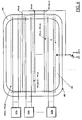
- the word line driver circuit section 113 is made up of a plurality of word line driver circuit blocks 113a - 113p . Each word line driver circuit block 113a - 113p is associated with a respective group of word lines of the array 101 . Only two word line driver circuit blocks 113a , 113p are shown in the drawing for simplicity: the word driver circuit block 113a is associated with the group of word lines WL1 to WLh , the word line driver circuit block 113p is associated with the group of word lines WLk to WLm . Each word line driver circuit block 113a - 113p receives from the row address decoder circuit section 111 a respective group WLSa - WLSp of word line selection control signal lines. The logic state on the word line selection control signal lines of each group WLSa - WLSp determines the selection or the deselection of the word lines of the corresponding word line group.
- each word line driver circuit block 113a - 113p is formed in a respective complementary doped semiconductor well structure 115a - 115p distinct from the doped semiconductor well structures in which the other word line driver circuit blocks are formed.
- Each doped semiconductor well structure 115a - 115p comprises a doped semiconductor well 117a - 117p of a second conductivity type, particularly of the N type in the shown example, formed in the semiconductor substrate 107.
- a respective doped semiconductor well 119a-119p of a first conductivity type, particularly of the P type in the shown example is formed.
- the first-conductivity-type semiconductor well 119a - 119p accommodates second-conductivity-type-channel MOSFETs (N-channel MOSFETs, in the shown example) of the respective word line driver circuit block, and the second-conductivity-type semiconductor well 117a - 117p accommodates first-conductivity-type-channel MOSFETs (P-channel MOSFETs, in the shown example) of the respective word line driver circuit block.
- the first-conductivity-type semiconductor well 119a - 119p that is formed in a given second-conductivity-type semiconductor well 117a - 117p needs not be physically continuous: more than one first-conductivity-type semiconductor wells 119a - 119p might be formed within a respective second-conductivity-type semiconductor well 117a - 117p .
- the second-conductivity-type semiconductor well 117a - 117p of a given doped semiconductor well structure may be physically made up of several wells.
- bias control circuits for biasing the doped semiconductor well structures 115a - 115p and for supplying the word line driver circuit blocks 113a - 113p with suitable supply voltages.
- Each bias control circuit 121a-121p controls a respective word line driver circuit block 113a - 113p and the doped semiconductor well structure 115a - 115p in which the respective word line driver circuit block is formed.
- the bias control circuits 121a - 121p bias the first- and second-conductivity-type semiconductor wells 119a - 119p and 117a - 117p of each doped semiconductor well structure 115a - 115p to respective, prescribed electric potentials, which depend on the memory operation mode.
- Each bias control circuit 121a - 121p receives a plurality of different electric potentials through voltage supply lines schematically indicated by a line VSUP in FIG. 1 .
- the different electric potentials are generated internally to the memory by circuits schematized as a block 123 , including for example positive and negative charge pumps.
- the circuits in the block 123 generates the different electric potentials starting from two supply voltages VDD and GND supplied to the memory (in which case the memory can be referred to as a Single Power Supply or SPS device).
- the memory includes control circuits schematized by a block 125 for controlling the memory operating mode; operating mode control signals identified altogether by a line MODE are supplied to the bias control circuits 121a-121p.
- the bias control circuits 121a - 121p also receives from the row address decoder circuit section 111 word line group selection signals DECa - DECp .
- One of the word line group selection signals DECa - DECp is asserted when a word line belonging to the respective group of word lines WL1-WLh,..., WLk - WLm is selected.
- the memory also comprises circuits, schematized in FIG. 1 as a block 127 , for biasing the semiconductor wells 103 and 105 in which the array of memory cells MC is formed, according to the memory operating mode.
- FIG. 3 wherein a circuit diagram is shown of a word line driver circuit block 113a of the plurality of word line driver circuit blocks 113a - 113p according to an embodiment of the invention.
- the word line driver circuit block comprises a plurality of word line driver circuits 3011 , 3012 ,... equal in number to the number of word lines of the respective group of word lines WL1-WLh . Only two word line driver circuits 3011 and 3012 are shown for simplicity.
- Each word line driver circuit 3011, 3012,... of a word line driver circuit block drives a respective word line of the group of word lines associated with the word line driver circuit block.
- Each word line driver circuit comprises a P-channel MOSFET P1 and an N-channel MOSFET N1 connected in series to each other in a CMOS inverter configuration between a first supply voltage line SPa and a second supply voltage line DECSa , which are common to all the word line driver circuits of the word line driver circuit block 113a .
- the P-channel and N-channel MOSFETs P1 and N1 are controlled by a word line selection signal carried by a word line selection signal line WLSa1, WLSa2, ... belonging to the respective group of word line selection signal lines WLSa.
- An output of the CMOS inverter P1, N1 is connected to a respective word line WL1, WL2,... of the group of word line WL1 - WLh.
- a given word line is selected when the voltage of the respective word line selection signal line is such as to turn the P-channel MOSFET P1 on, thereby the word line potential is brought to that of the first supply voltage line SPa .
- the word line is deselected when the voltage of the respective word line selection signal line is such as to turn the N-channel MOSFET N1 on, thereby the word line potential is brought to that of the second supply voltage line DECSa.
- the P-channel MOSFETs P1 of all the word line driver circuits 3011 , 3012 of a same word line driver circuit block 113a - 113p are formed within the N-type semiconductor well 117a - 117p of the respective doped semiconductor well structure 115a - 115p .
- the N-channel MOSFETs N1 of all the word line driver circuits 3011 , 3012 of a same word line driver circuit block 113a - 113p are formed within the P-type semiconductor well 119a - 119p of the respective doped semiconductor well structure 115a - 115p.
- the first and second supply voltage lines SPa - SPp and DECSa - DECSp of each word line driver circuit block 113a-113p are controlled by the respective bias control circuit 121a - 121p .
- the bias control circuits 121a - 121p also control the biasing of the associated N-type and P-type semiconductor wells 117a - 117p and 119a - 119p to the prescribed electric potentials, as will be discussed in detail later on, through respective doped semiconductor well bias voltage lines DECNa - DECNp and DECPa - DECPp .
- FIG. 4 is a schematic diagram of a bias control circuit 121a of the plurality of bias control circuits 121a - 121p according to an embodiment of the present invention.
- the bias control circuit 121a receives from the internal voltage generator 123 six different potentials, namely: a reference potential VREF, for example equal to the ground voltage GND externally supplied to the memory; a first positive potential VPOS1, for example equal to 4.5 V; a second positive potential VPOS2 , for example equal 5 V; a third positive potential VPOS3 , for example equal to 8.5 V; a first negative potential VNEG1, for example equal to -8 V; and a second negative potential VNEG2 , for example equal to -9 V.
- a reference potential VREF for example equal to the ground voltage GND externally supplied to the memory
- a first positive potential VPOS1 for example equal to 4.5 V
- VPOS2 for example equal 5 V
- a third positive potential VPOS3 for example equal to 8.5 V
- a second negative potential VNEG2 for example equal to -9 V.
- the operating mode control signals MODE include a read mode signal RD asserted when the memory is operated in read mode, a program mode signal PG asserted when the memory is operated in program mode, and an erase mode signal ER asserted when the memory is operated in erase mode.
- the first voltage supply signal line SPa of the word line driver circuits of the word line driver circuit block 113a can be selectively switched to the reference potential VREF, the first positive potential VPOS1 and the third positive potential VPOS3.
- a first switch SW1 controlled by a signal 405 which is asserted when the program mode signal PG is asserted and the word line group selection signal DECa is asserted, connects the first voltage supply signal line SPa to the third positive potential VPOS3 when the memory is in program mode and the word line to be programmed belongs to the word line group associated with the bias control circuit 121a .
- the first switch SW1 connects the first voltage supply line SPa to an output of a second switch SW2 switchable between the reference potential VREF and the first positive potential VPOS1.
- the second switch SW2 is controlled by a signal 401 which is asserted when the memory is in read mode (read mode signal RD asserted) or when the memory is in erase mode (erase mode signal ER asserted) but the group of word lines associated with the bias control circuit 121a is not selected (signal DECa is deasserted); when signal 401 is asserted, the second switch SW2 is turned to the first positive potential VPOS1, otherwise the second switch SW2 is turned to the reference potential VREF.
- a signal 401 which is asserted when the memory is in read mode (read mode signal RD asserted) or when the memory is in erase mode (erase mode signal ER asserted) but the group of word lines associated with the bias control circuit 121a is not selected (signal DECa is deasserted); when signal 401 is asserted, the second switch SW2 is turned to the first positive potential VPOS1, otherwise the second switch SW2 is turned to the reference potential VREF.
- the second voltage supply signal line DECSa of the word line driver circuits of the word line driver circuit block 113a can be selectively switched between the reference potential VREF and the first negative potential VNEG1.
- a third switch SW3 controlled by a signal 403 allows to connect the second voltage supply signal line DECSa to the reference potential VREF unless the memory is in erase mode (erase mode signal ER asserted) and the group of word lines associated with the bias control circuit 121a is selected (signal DECa asserted), in which case the second voltage supply signal line DECSa is connected to the first negative potential VNEG1 .
- the P-well bias signal line DECPa can be selectively switched between the reference potential VREF and the second negative potential VNEG2, through a fourth switch SW4 controlled by the signal 403.
- the P-well bias signal line DECPa is connected to the reference potential VREF unless the memory is in erase mode (signal ER asserted) and the group of word lines associated with the bias control circuit 121a is selected (signal DECa asserted), in which case the P-well bias signal line DECPa is connected to the second negative potential VNEG2.
- the N-well bias signal line DECNa can be selectively switched to the reference potential VREF, the second positive potential VPOS2 and the third positive potential VPOS3.
- a fifth switch SW5, controlled by the signal 405 connects the N-well bias signal line DECNa to the third positive potential VPOS3 when the program mode signal PG is asserted, i.e. when the memory is in program mode, and the word line to be programmed belongs to the word line group associated with the bias control circuit 121a .
- the fifth switch SW5 connects the N-well bias signal line DECNa to an output of a sixth switch SW6 switchable between the reference potential VREF and the second positive potential VPOS2 .
- the sixth switch SW6 is controlled by the signal 401, so as to connect the N-well bias signal line DECNa to the second positive potential VPOS2 when the memory is in read mode (read mode signal RD asserted) or when the memory is in erase mode (erase mode signal ER asserted) but the group of word lines associated with the bias control circuit 121a is not selected (signal DECa is deasserted), and to the reference potential VREF when the memory is in erase mode and the word line to be erased belongs to the word line group associated with the bias control circuit 121a .
- bias control circuits 121a-121p are clearly possible.
- FIGS. 5A, 5B and 5c schematically show the exemplary electric potentials described above applied to the N-type and P-type wells of the word line selector and of the array of memory cells, as well as to the word lines, in the read, program and erase operating modes, respectively.
- all the N-type semiconductor wells 117a - 117p are biased to the second positive potential VPOS2 , e.g. 5 V; all the P-type semiconductor wells 119a - 119p are biased to the reference potential VREF (0 V).
- the P-type well 103 in which the memory cells MC are formed is biased to the reference potential VREF, and the N-type well 105 is biased to the second positive potential VPOS2 (5 V).
- the selected word line WLSEL is biased to the first positive potential VPOS1, e.g. 4.5 V; the remaining, non-selected word lines WLNSEL1, WLSEL2 are kept at the reference potential VREF , irrespective of the word line group to which they belong.
- At least the N-type semiconductor well 117a associated with the word line selected for programming is biased to the third positive potential VPOS3, e.g. 8.5 V, while all the other N-type semiconductor wells are biased to the same positive potential used in the read operating mode, i.e. the second positive potential VPOS2 (5 V); alternatively, all the N-type semiconductor wells 117a - 117p are biased to the third positive potential VPOS3. All the P-type semiconductor wells 119a - 119p are biased to the reference potential VREF.
- the P-type well 103 in which the memory cells MC are formed is biased to the reference potential VREF
- the N-type well 105 is biased to the second positive potential VPOS2.
- the P-type well 103 could be biased to a slightly negative potential, e.g. ranging from -1 V to -2 V.
- the word line WLSEL selected for programming is biased to the third positive potential VPOS3 (8.5 V), while all the other, non-selected word lines WLNSEL1, WLNSEL2 are biased to the reference potential VREF , irrespective of the word line group to which they belong.
- the P-type well 103 in which the memory cells MC are formed and the N-type well 105 are biased to the third positive potential VPOS3 (8.5 V) .
- the word line WLSEL selected for being erased belongs to the group of word lines WL1 - WLh
- the N-type semiconductor well 117a is biased to the reference potential VREF
- the P-type semiconductor well 119a is biased to the second negative potential VNEG2 (-9 V).
- the word line WLSEL to be erased is biased to the first negative potential VNEG1 (-8 V), while all the other, non-selected word lines WLNSEL1 of the same group WL1 - WLh are biased to the reference potential VREF. All the other N-type semiconductor wells (such as the N-type semiconductor well 117p in the drawing) are biased to the second positive potential (5 V), and the respective P-type semiconductor wells (such as the P-type well 119p in the drawing) are biased to the reference potential VREF. The non-selected word lines WLNSEL2 belonging to the other groups of word lines are biased to the first positive potential VPOS1 (4.5 V).
- the memory cells belonging to the other, non-selected word lines WLSEL1 of the same word line group as the selected word line WLSEL are submitted to a gate-to-bulk voltage equal to -8.5 V.
- the positive potential VPOS3 (8.5 V) is applied to the P-type well 103 progressively, for example ramping up the voltage applied to the P-type well 103 from an initial value of 3 or 4 V to the full 8.5 V. This avoids a peak in the Fowler-Nordheim current.
- the memory cells of the non-selected word lines of word line groups different from that containing the selected word line could be biased to a potential even higher than 4.5 V, e.g. up to the positive potential to which the P-type well 103 is biased (8.5 V); to this purpose, it suffices to bias the P-type and N-type wells in which the respective word line drivers are formed to 0 V and 8.5 V, respectively, and connecting the respective first voltage supply lines to the 8.5 V potential.
- a refresh procedure of the memory cells of the word lines belonging to the same group as the erased word line can be provided for, so as to avoid that these memory cells loose the data stored therein.
- the electric potentials applied to word lines belonging to different word line groups can be completely uncorrelated.
- the erase mode it is thus possible to bias the word lines not to be erased and belonging to different word line groups to an erase inhibition potential, intermediate between the reference potential and the potential of the P-type well 103 in which the memory cells are formed, or even equal to the potential of the P-type well 103 .
- more than one word line could be simultaneously selected for erasing: this depends on how fine an erase granularity is desired for the memory.
- the word lines to be simultaneously erased may belong to a same word line group or even to different word line groups; clearly, in the latter case more memory cells will be disturbed during the erase operation.
- each word line group should contain the minimum possible number of word lines.
- every word line driver circuit could be formed within a respective doped semiconductor well structure, physically separated from the doped semiconductor well structures of the other word line driver circuits. In this way, all the word lines except the one selected for erasure could be biased to the erase inhibition potential. This however would have a non-negligible impact on the overall chip area occupied by the word line selector.
- the number of word lines of a given group should not be too high, not to excessively lengthen the time required for refreshing the memory cells of the word line group. The number of word lines in each group can thus be determined as a trade off between the chip area overhead and the time required to refresh the memory cells of a given word line group.
- the present invention allows implementing a refresh procedure according to which all the memory cells of a given word line group are refreshed each time a word line of the word line group is erased. This is clearly advantageous compared to refresh procedures in which memory cells are refreshed only on a periodical basis.
- Another advantage of the present invention is the increase in the memory endurance even when no data refresh schemes are implemented. Compared to a memory equipped with a conventional word line selector, the number of erase disturbs to which the memory cells of any word line of the array are subject is reduced of a factor equal to the number of word line groups.
- word lines belonging to a same word line group need not be physically adjacent.
- space optimization and signal line routing considerations could lead to a layout arrangement such that word line driver circuits formed in a same complementary doped semiconductor well structure drive alternate word lines of the array.
- the memory may comprise two or more arrays 101 , of equal or different size, each one formed in a respective P-type well 103 .
- Each array forms a memory sector, and has associated therewith a respective word line selector.
- FIG. 6 schematically shows a memory cell array embodiment allowing to avoid this problem.
- At least one dummy word line WLd1 - WLd(p-1), not belonging to any of the word line groups, is inserted in the memory cell array between adjacent word line groups (WL1 - WLh ) , (WL(h+1) - WLj),..., (WLk - WLm ).
- the dummy word lines WLd - WL(p-1) can for example be biased to the same electric potentials as the P-type well 103 , which means that, according to the example provided above, both the potential of the P-type well 103 and that of the dummy word lines WLd1 - WLd(p-1) can be selectively switched between 0 V and 8.5 V, depending on the memory operating mode.
- a pair of dummy word lines are inserted between each pair of adjacent word line groups.
- the present invention also set forth a new scheme of memory sectorization.
- the different word line groups can be viewed as different "logical" memory sectors. Memory cells belonging to a same logical memory sector can be erased independently from the other logical memory sectors: all the word lines of a logical memory sector are to this purpose biased to the erase potential (by selecting all the word lines of the word line group), while the word lines of the other logical memory sectors are biased to the erase inhibition potential.
- Conventional memory sectorization schemes calls for forming different memory cell arrays in physically distinct and isolated P-type wells 103, with a bit line structure made up of main bit lines common to the whole memory and local bit lines local to each memory sector, and switches for selectively connecting the local bit lines to the main bit lines.
- the sectorization scheme according to the present invention allows reducing the semiconductor chip area, because a single memory cell array can be formed in a unique semiconductor well. Area is also saved since there is no necessity of introducing main bit lines and local bit lines and corresponding switches.
- FIG. 7 schematically shows another embodiment of memory in which the word line selector according to the present invention can advantageously be used.
- a plurality of P-type doped semiconductor stripes 703a - 703t is provided.
- the P-type stripes 703a - 703t extend within the N-type well 105 parallelly to the columns of memory cells and thus transversally to the array word lines WL1 - WLm.
- each bit line group includes the bit lines whose memory cells are formed in a same P-type stripe 703a - 703t .
- a P-type stripe bias circuit 705 is provided; the P-type stripe bias circuit 705 , on the basis of a P-type stripe address carried by P-type address signal lines STADD derived from the address signal line bus ADD, allows selectively biasing the P-type stripes 703a-703t through P-type stripe bias lines 705a - 705t .
- the provision of the plurality of P-type stripes 703a - 703t allows submitting to erasure selected portions of a word line of memory cells, instead of a whole word line.
- the P-type stripe in which the memory cells of the selected portion of word line are formed is biased as in FIG. 5C to a positive potential of, e.g. , 8.5 V, while the remaining P-type stripes are kept to ground. In this way, an even finer erase granularity is achieved.
- This array structure in conjunction with the word line selector according to the present invention, allows further limiting the number of memory cells subjected to disturbs during an erase operation: only the memory cells of the same word line group WL1 - WLh ,..., WLk - WLm as the selected word line and formed in the same P-type stripe as the memory cells of the selected word line portion are subjected to disturbs.
- dummy word lines are preferably provided between adjacent word line groups.
Landscapes
- Engineering & Computer Science (AREA)
- Microelectronics & Electronic Packaging (AREA)
- Read Only Memory (AREA)
- Non-Volatile Memory (AREA)
Abstract
Description
Claims (12)
- A word line selector for selecting word lines (WL1-WLm) of an array (101) of semiconductor memory cells (MC) formed in a doped semiconductor region (103) of a semiconductor substrate (107), comprising a plurality of word line drivers (3011,3012) responsive to word line selection signals (WLSa1,WLSa2), each word line driver being associated with a respective word line for driving the word line to prescribed word line electric potentials according to the word line selection signals, said word line electric potentials depending on an operation to be conducted on the array of memory cells,
characterized in that a plurality of distinct doped semiconductor well structures (115a - 115p) is provided in the semiconductor substrate, each doped semiconductor well structure accommodating a respective group (113a - 113p) of at least one word line driver associated with a respective group (WL1-WLh,WLk-WLm) of at least one word line. - The word line selector according to claim 1, further comprising a word line address decoder (111) for decoding word line addresses (RADD) identifying the word lines and accordingly controlling the word line selection signals.
- The word line selector according to claim 2, further comprising doped semiconductor well structure biasing means (121a-121p) for selectively biasing (DECNa,DECPa-DECNp,DECPp) each doped semiconductor well structure to respective prescribed doped semiconductor well bias potentials, dependent on the operation to be conducted on the array of memory cells.
- The word line selector according to claim 3, in which at least one word line (WLSEL) in at least one word line group is selected during a memory cell erase operation.
- The word line selector according to claim 4, in which in the erase operation:the word line driver associated with the selected word line biases the selected word line to an erase word line potential (VNEG1) ;the doped semiconductor well structure biasing means biases the doped semiconductor well structure accomodating the word line driver group associated with the group of word lines including the selected word line to a semiconductor well bias potential compatible with the erase word line potential;the word line drivers associated with groups of word lines not including the selected word line bias the respective word lines (WLNSEL2) to an erase inhibition word line potential (VPOS1) ;the semiconductor well structure biasing means biases the doped semiconductor well structures accomodating the word line driver groups associated with the groups of word lines not including the selected word line to a semiconductor well bias potential compatible with the erase inhibition word line potential.
- The word line selector according to claim 5, in which in the erase operation of memory cells belonging to a selected word line the word line drivers associated with the non-selected word lines (WLNSEL1) belonging to the same group of word lines as the selected word line bias the respective word lines to an intermediate word line potential (VREF) intermediate between the erase potential and the erase inhibition potential, thereby the memory cells belonging to the non-selected word lines are not erased.
- The word line selector according to claim 5, in which in the erase operation of memory cells belonging to a selected word line the word line drivers associated with the non-selected word lines (WLNSEL1) belonging to the same group of word lines as the selected word line bias the respective word lines to the erase potential, thereby also the memory cells belonging to the non-selected word lines are erased.
- The word line selector according to any one of the preceding claims, in which each doped semiconductor well structure comprises at least one first doped semiconductor well (117a-117p) of a first conductivity type formed in the semiconductor substrate, and at least one second doped semiconductor well (119a-119p) of a second conductivity type formed in the at least one first semiconductor well, the first and second semiconductor wells respectively accommodating first (P1) and second (N1) types of transistors of the word line drivers.
- A semiconductor memory comprising at least one array (101) of memory cells (MC) having a plurality of memory cell word lines (WL1 - WLm), and word line selection means (108) associated with the array for selecting the memory cell word lines, characterized in that the word line selection means include a word line selector according to any one of claims 1 to 8.
- The semiconductor memory according to claim 9, in which the array of memory cells includes dummy word lines (WLd1-WLd(p-1)) of memory cells, at least one dummy word line being inserted between adjacent word line groups.
- The semiconductor memory according to claim 9 or 10, in which the array of memory cells includes a plurality of logical memory sectors, each logical memory sector being formed by word lines of a same word line group.
- The semiconductor memory according to any one of claims 9 to 11, in which a plurality of electrically independent doped semiconductor regions (703a-703t) are provided, each one accommodating a respective group of memory cells of the array, the doped semiconductor regions defining in each word line individually erasable word line portions.
Priority Applications (3)
| Application Number | Priority Date | Filing Date | Title |
|---|---|---|---|
| EP02425084A EP1339069B1 (en) | 2002-02-20 | 2002-02-20 | Word line selector for a semiconductor memory |
| DE60200715T DE60200715D1 (en) | 2002-02-20 | 2002-02-20 | Selecteur à ligne des mots pour une memoire semiconductrice |
| US10/372,626 US6865114B2 (en) | 2002-02-20 | 2003-02-20 | Word line selector for a semiconductor memory |
Applications Claiming Priority (1)
| Application Number | Priority Date | Filing Date | Title |
|---|---|---|---|
| EP02425084A EP1339069B1 (en) | 2002-02-20 | 2002-02-20 | Word line selector for a semiconductor memory |
Publications (2)
| Publication Number | Publication Date |
|---|---|
| EP1339069A1 true EP1339069A1 (en) | 2003-08-27 |
| EP1339069B1 EP1339069B1 (en) | 2004-07-07 |
Family
ID=27635926
Family Applications (1)
| Application Number | Title | Priority Date | Filing Date |
|---|---|---|---|
| EP02425084A Expired - Lifetime EP1339069B1 (en) | 2002-02-20 | 2002-02-20 | Word line selector for a semiconductor memory |
Country Status (3)
| Country | Link |
|---|---|
| US (1) | US6865114B2 (en) |
| EP (1) | EP1339069B1 (en) |
| DE (1) | DE60200715D1 (en) |
Cited By (1)
| Publication number | Priority date | Publication date | Assignee | Title |
|---|---|---|---|---|
| US6865114B2 (en) | 2002-02-20 | 2005-03-08 | Stmicroelectronics, S.R.L. | Word line selector for a semiconductor memory |
Families Citing this family (19)
| Publication number | Priority date | Publication date | Assignee | Title |
|---|---|---|---|---|
| US7423304B2 (en) * | 2003-12-05 | 2008-09-09 | Sandisck 3D Llc | Optimization of critical dimensions and pitch of patterned features in and above a substrate |
| ITMI20050868A1 (en) * | 2005-05-13 | 2006-11-14 | St Microelectronics Srl | ROW DECODING CIRCUIT |
| US7499307B2 (en) * | 2005-06-24 | 2009-03-03 | Mosys, Inc. | Scalable embedded DRAM array |
| US7274618B2 (en) * | 2005-06-24 | 2007-09-25 | Monolithic System Technology, Inc. | Word line driver for DRAM embedded in a logic process |
| US7397708B2 (en) * | 2005-08-03 | 2008-07-08 | Infineon Technologies Ag | Technique to suppress leakage current |
| US7403418B2 (en) * | 2005-09-30 | 2008-07-22 | Silicon Storage Technology, Inc. | Word line voltage boosting circuit and a memory array incorporating same |
| KR100749737B1 (en) * | 2006-01-25 | 2007-08-16 | 삼성전자주식회사 | NOR flash memory and its erasing method |
| JP2007207380A (en) * | 2006-02-03 | 2007-08-16 | Renesas Technology Corp | Nonvolatile semiconductor memory device |
| US8892806B2 (en) * | 2007-03-07 | 2014-11-18 | Intel Mobile Communications GmbH | Integrated circuit, memory device, method of operating an integrated circuit, and method of designing an integrated circuit |
| KR100897603B1 (en) * | 2007-06-20 | 2009-05-14 | 삼성전자주식회사 | Semiconductor memory device |
| KR100882205B1 (en) * | 2007-06-27 | 2009-02-06 | 삼성전자주식회사 | Nonvolatile memory device that reduces layout area of global wordline decoder and its operation method |
| KR101489885B1 (en) * | 2007-11-21 | 2015-02-06 | 삼성전자주식회사 | Charge Trap Nonvolatile Memory Device With Enhanced Reliability And Method Of Operating The Same |
| US20140307504A1 (en) * | 2013-04-12 | 2014-10-16 | Winbond Electronics Corp. | Data storage device, and fabrication and control methods thereof |
| US9558114B2 (en) * | 2013-06-03 | 2017-01-31 | Infineon Technologies Ag | System and method to store data in an adjustably partitionable memory array |
| FR3033076B1 (en) | 2015-02-23 | 2017-12-22 | St Microelectronics Rousset | NON-VOLATILE MEMORY HAVING VARIABLE POLARITY LINE DECODER |
| ITUB20151112A1 (en) * | 2015-05-27 | 2016-11-27 | St Microelectronics Srl | NON-VOLATILE MEMORY DEVICE AND CORRESPONDING STRESS-REDUCING OPERATION METHOD |
| US10331838B2 (en) * | 2016-12-12 | 2019-06-25 | Taiwan Semiconductor Manufacturing Co., Ltd. | Semiconductor device with fill cells |
| US10734048B2 (en) | 2018-06-05 | 2020-08-04 | Sandisk Technologies Llc | Sensing memory cells using array control lines |
| US11404123B1 (en) * | 2021-04-05 | 2022-08-02 | Sandisk Technologies Llc | Non-volatile memory with multiple wells for word line switch transistors |
Citations (4)
| Publication number | Priority date | Publication date | Assignee | Title |
|---|---|---|---|---|
| EP0606650A2 (en) * | 1993-01-13 | 1994-07-20 | Kabushiki Kaisha Toshiba | Nonvolatile semiconductor memory device |
| US5822252A (en) * | 1996-03-29 | 1998-10-13 | Aplus Integrated Circuits, Inc. | Flash memory wordline decoder with overerase repair |
| US5847994A (en) * | 1997-09-08 | 1998-12-08 | Mitsubishi Denki Kabushiki Kaisha | Non-volatile semiconductor memory device having a back ground operation mode |
| US5931563A (en) * | 1996-12-10 | 1999-08-03 | Nec Corporation | Method and device for erasing non-volatile semiconductor memory with smaller erase variation |
Family Cites Families (3)
| Publication number | Priority date | Publication date | Assignee | Title |
|---|---|---|---|---|
| JPH10144879A (en) * | 1996-11-06 | 1998-05-29 | Toshiba Corp | Word line driver circuit and semiconductor memory device |
| JP3762114B2 (en) * | 1998-09-08 | 2006-04-05 | 株式会社東芝 | Nonvolatile semiconductor memory device |
| EP1339069B1 (en) | 2002-02-20 | 2004-07-07 | STMicroelectronics S.r.l. | Word line selector for a semiconductor memory |
-
2002
- 2002-02-20 EP EP02425084A patent/EP1339069B1/en not_active Expired - Lifetime
- 2002-02-20 DE DE60200715T patent/DE60200715D1/en not_active Expired - Lifetime
-
2003
- 2003-02-20 US US10/372,626 patent/US6865114B2/en not_active Expired - Lifetime
Patent Citations (4)
| Publication number | Priority date | Publication date | Assignee | Title |
|---|---|---|---|---|
| EP0606650A2 (en) * | 1993-01-13 | 1994-07-20 | Kabushiki Kaisha Toshiba | Nonvolatile semiconductor memory device |
| US5822252A (en) * | 1996-03-29 | 1998-10-13 | Aplus Integrated Circuits, Inc. | Flash memory wordline decoder with overerase repair |
| US5931563A (en) * | 1996-12-10 | 1999-08-03 | Nec Corporation | Method and device for erasing non-volatile semiconductor memory with smaller erase variation |
| US5847994A (en) * | 1997-09-08 | 1998-12-08 | Mitsubishi Denki Kabushiki Kaisha | Non-volatile semiconductor memory device having a back ground operation mode |
Non-Patent Citations (1)
| Title |
|---|
| AKIRA UMEZAWA ET AL: "A 5-V-ONLY OPERATION 0.6-UM FLASH EEPROM WITH ROW DECODER SCHEME IN TRIPLE-WELL STRUCTURE", IEEE JOURNAL OF SOLID-STATE CIRCUITS, IEEE INC. NEW YORK, US, vol. 27, no. 11, 1 November 1992 (1992-11-01), pages 1540 - 1545, XP000320440, ISSN: 0018-9200 * |
Cited By (1)
| Publication number | Priority date | Publication date | Assignee | Title |
|---|---|---|---|---|
| US6865114B2 (en) | 2002-02-20 | 2005-03-08 | Stmicroelectronics, S.R.L. | Word line selector for a semiconductor memory |
Also Published As
| Publication number | Publication date |
|---|---|
| US20030198101A1 (en) | 2003-10-23 |
| DE60200715D1 (en) | 2004-08-12 |
| US6865114B2 (en) | 2005-03-08 |
| EP1339069B1 (en) | 2004-07-07 |
Similar Documents
| Publication | Publication Date | Title |
|---|---|---|
| EP1339069B1 (en) | Word line selector for a semiconductor memory | |
| US6917544B2 (en) | Multiple use memory chip | |
| US6614070B1 (en) | Semiconductor non-volatile memory device having a NAND cell structure | |
| US10460807B2 (en) | Integrated erase voltage path for multiple cell substrates in nonvolatile memory devices | |
| US6163048A (en) | Semiconductor non-volatile memory device having a NAND cell structure | |
| US7298647B2 (en) | Operating techniques for reducing program and read disturbs of a non-volatile memory | |
| US6392933B1 (en) | EEPROM erasing method | |
| KR100331563B1 (en) | NAND-type flash memory device and method for operating the same | |
| US6570787B1 (en) | Programming with floating source for low power, low leakage and high density flash memory devices | |
| JP3659205B2 (en) | Nonvolatile semiconductor memory device and driving method thereof | |
| CN114616625B (en) | Four-gate split-gate flash memory array with byte erase operation | |
| US9443594B2 (en) | Logic embedded nonvolatile memory device | |
| US8462559B2 (en) | Memory erase methods and devices | |
| KR19980017439A (en) | Flash memory device and driving method thereof | |
| JP3640177B2 (en) | Nonvolatile semiconductor memory device | |
| JP3640180B2 (en) | Nonvolatile semiconductor memory device | |
| US7304890B2 (en) | Double byte select high voltage line for EEPROM memory block | |
| KR100639827B1 (en) | 1 transistor cell for EEPROM applications | |
| KR100370890B1 (en) | Nonvolatile semiconductor memory device | |
| US6888754B2 (en) | Nonvolatile semiconductor memory array with byte-program, byte-erase, and byte-read capabilities | |
| US12380932B2 (en) | Row decoder and row address scheme in a memory system | |
| EP1256116B1 (en) | Flash memory architecture employing three layer metal interconnect | |
| JP2006196700A (en) | Nonvolatile semiconductor memory device | |
| JPH0660679A (en) | Nonvolatile semiconductor memory device | |
| US6819593B2 (en) | Architecture to suppress bit-line leakage |
Legal Events
| Date | Code | Title | Description |
|---|---|---|---|
| PUAI | Public reference made under article 153(3) epc to a published international application that has entered the european phase |
Free format text: ORIGINAL CODE: 0009012 |
|
| AK | Designated contracting states |
Designated state(s): AT BE CH CY DE DK ES FI FR GB GR IE IT LI LU MC NL PT SE TR |
|
| AX | Request for extension of the european patent |
Extension state: AL LT LV MK RO SI |
|
| GRAP | Despatch of communication of intention to grant a patent |
Free format text: ORIGINAL CODE: EPIDOSNIGR1 |
|
| 17P | Request for examination filed |
Effective date: 20030822 |
|
| GRAS | Grant fee paid |
Free format text: ORIGINAL CODE: EPIDOSNIGR3 |
|
| AKX | Designation fees paid |
Designated state(s): DE FR GB IT |
|
| GRAA | (expected) grant |
Free format text: ORIGINAL CODE: 0009210 |
|
| AK | Designated contracting states |
Kind code of ref document: B1 Designated state(s): DE FR GB IT |
|
| REG | Reference to a national code |
Ref country code: GB Ref legal event code: FG4D |
|
| REG | Reference to a national code |
Ref country code: IE Ref legal event code: FG4D |
|
| REF | Corresponds to: |
Ref document number: 60200715 Country of ref document: DE Date of ref document: 20040812 Kind code of ref document: P |
|
| PG25 | Lapsed in a contracting state [announced via postgrant information from national office to epo] |
Ref country code: DE Free format text: LAPSE BECAUSE OF FAILURE TO SUBMIT A TRANSLATION OF THE DESCRIPTION OR TO PAY THE FEE WITHIN THE PRESCRIBED TIME-LIMIT Effective date: 20041008 |
|
| PLBE | No opposition filed within time limit |
Free format text: ORIGINAL CODE: 0009261 |
|
| STAA | Information on the status of an ep patent application or granted ep patent |
Free format text: STATUS: NO OPPOSITION FILED WITHIN TIME LIMIT |
|
| ET | Fr: translation filed | ||
| 26N | No opposition filed |
Effective date: 20050408 |
|
| PGFP | Annual fee paid to national office [announced via postgrant information from national office to epo] |
Ref country code: IT Payment date: 20080212 Year of fee payment: 7 |
|
| PGFP | Annual fee paid to national office [announced via postgrant information from national office to epo] |
Ref country code: GB Payment date: 20090128 Year of fee payment: 8 |
|
| PGFP | Annual fee paid to national office [announced via postgrant information from national office to epo] |
Ref country code: FR Payment date: 20090226 Year of fee payment: 8 |
|
| GBPC | Gb: european patent ceased through non-payment of renewal fee |
Effective date: 20100220 |
|
| REG | Reference to a national code |
Ref country code: FR Ref legal event code: ST Effective date: 20101029 |
|
| PG25 | Lapsed in a contracting state [announced via postgrant information from national office to epo] |
Ref country code: FR Free format text: LAPSE BECAUSE OF NON-PAYMENT OF DUE FEES Effective date: 20100301 |
|
| PG25 | Lapsed in a contracting state [announced via postgrant information from national office to epo] |
Ref country code: GB Free format text: LAPSE BECAUSE OF NON-PAYMENT OF DUE FEES Effective date: 20100220 Ref country code: IT Free format text: LAPSE BECAUSE OF NON-PAYMENT OF DUE FEES Effective date: 20090220 |