EP1337135A2 - High frequency unit - Google Patents
High frequency unit Download PDFInfo
- Publication number
- EP1337135A2 EP1337135A2 EP03250777A EP03250777A EP1337135A2 EP 1337135 A2 EP1337135 A2 EP 1337135A2 EP 03250777 A EP03250777 A EP 03250777A EP 03250777 A EP03250777 A EP 03250777A EP 1337135 A2 EP1337135 A2 EP 1337135A2
- Authority
- EP
- European Patent Office
- Prior art keywords
- component
- high frequency
- frequency unit
- adhesive agent
- circuit substrate
- Prior art date
- Legal status (The legal status is an assumption and is not a legal conclusion. Google has not performed a legal analysis and makes no representation as to the accuracy of the status listed.)
- Withdrawn
Links
Images



Classifications
-
- H—ELECTRICITY
- H05—ELECTRIC TECHNIQUES NOT OTHERWISE PROVIDED FOR
- H05K—PRINTED CIRCUITS; CASINGS OR CONSTRUCTIONAL DETAILS OF ELECTRIC APPARATUS; MANUFACTURE OF ASSEMBLAGES OF ELECTRICAL COMPONENTS
- H05K1/00—Printed circuits
- H05K1/02—Details
-
- H—ELECTRICITY
- H05—ELECTRIC TECHNIQUES NOT OTHERWISE PROVIDED FOR
- H05K—PRINTED CIRCUITS; CASINGS OR CONSTRUCTIONAL DETAILS OF ELECTRIC APPARATUS; MANUFACTURE OF ASSEMBLAGES OF ELECTRICAL COMPONENTS
- H05K3/00—Apparatus or processes for manufacturing printed circuits
- H05K3/30—Assembling printed circuits with electric components, e.g. with resistors
- H05K3/303—Assembling printed circuits with electric components, e.g. with resistors with surface mounted components
- H05K3/305—Affixing by adhesive
-
- H—ELECTRICITY
- H10—SEMICONDUCTOR DEVICES; ELECTRIC SOLID-STATE DEVICES NOT OTHERWISE PROVIDED FOR
- H10W—GENERIC PACKAGES, INTERCONNECTIONS, CONNECTORS OR OTHER CONSTRUCTIONAL DETAILS OF DEVICES COVERED BY CLASS H10
- H10W76/00—Containers; Fillings or auxiliary members therefor; Seals
- H10W76/40—Fillings or auxiliary members in containers, e.g. centering rings
- H10W76/42—Fillings
- H10W76/47—Solid or gel fillings
-
- H—ELECTRICITY
- H05—ELECTRIC TECHNIQUES NOT OTHERWISE PROVIDED FOR
- H05K—PRINTED CIRCUITS; CASINGS OR CONSTRUCTIONAL DETAILS OF ELECTRIC APPARATUS; MANUFACTURE OF ASSEMBLAGES OF ELECTRICAL COMPONENTS
- H05K1/00—Printed circuits
- H05K1/18—Printed circuits structurally associated with non-printed electric components
- H05K1/181—Printed circuits structurally associated with non-printed electric components associated with surface mounted components
-
- H—ELECTRICITY
- H05—ELECTRIC TECHNIQUES NOT OTHERWISE PROVIDED FOR
- H05K—PRINTED CIRCUITS; CASINGS OR CONSTRUCTIONAL DETAILS OF ELECTRIC APPARATUS; MANUFACTURE OF ASSEMBLAGES OF ELECTRICAL COMPONENTS
- H05K2201/00—Indexing scheme relating to printed circuits covered by H05K1/00
- H05K2201/10—Details of components or other objects attached to or integrated in a printed circuit board
- H05K2201/10613—Details of electrical connections of non-printed components, e.g. special leads
- H05K2201/10621—Components characterised by their electrical contacts
- H05K2201/10734—Ball grid array [BGA]; Bump grid array
-
- H—ELECTRICITY
- H05—ELECTRIC TECHNIQUES NOT OTHERWISE PROVIDED FOR
- H05K—PRINTED CIRCUITS; CASINGS OR CONSTRUCTIONAL DETAILS OF ELECTRIC APPARATUS; MANUFACTURE OF ASSEMBLAGES OF ELECTRICAL COMPONENTS
- H05K2201/00—Indexing scheme relating to printed circuits covered by H05K1/00
- H05K2201/20—Details of printed circuits not provided for in H05K2201/01 - H05K2201/10
- H05K2201/2018—Presence of a frame in a printed circuit or printed circuit assembly
-
- H—ELECTRICITY
- H05—ELECTRIC TECHNIQUES NOT OTHERWISE PROVIDED FOR
- H05K—PRINTED CIRCUITS; CASINGS OR CONSTRUCTIONAL DETAILS OF ELECTRIC APPARATUS; MANUFACTURE OF ASSEMBLAGES OF ELECTRICAL COMPONENTS
- H05K2201/00—Indexing scheme relating to printed circuits covered by H05K1/00
- H05K2201/20—Details of printed circuits not provided for in H05K2201/01 - H05K2201/10
- H05K2201/2036—Permanent spacer or stand-off in a printed circuit or printed circuit assembly
-
- H—ELECTRICITY
- H05—ELECTRIC TECHNIQUES NOT OTHERWISE PROVIDED FOR
- H05K—PRINTED CIRCUITS; CASINGS OR CONSTRUCTIONAL DETAILS OF ELECTRIC APPARATUS; MANUFACTURE OF ASSEMBLAGES OF ELECTRICAL COMPONENTS
- H05K2203/00—Indexing scheme relating to apparatus or processes for manufacturing printed circuits covered by H05K3/00
- H05K2203/11—Treatments characterised by their effect, e.g. heating, cooling, roughening
- H05K2203/1147—Sealing or impregnating, e.g. of pores
-
- H—ELECTRICITY
- H05—ELECTRIC TECHNIQUES NOT OTHERWISE PROVIDED FOR
- H05K—PRINTED CIRCUITS; CASINGS OR CONSTRUCTIONAL DETAILS OF ELECTRIC APPARATUS; MANUFACTURE OF ASSEMBLAGES OF ELECTRICAL COMPONENTS
- H05K3/00—Apparatus or processes for manufacturing printed circuits
- H05K3/30—Assembling printed circuits with electric components, e.g. with resistors
- H05K3/301—Assembling printed circuits with electric components, e.g. with resistors by means of a mounting structure
-
- H—ELECTRICITY
- H10—SEMICONDUCTOR DEVICES; ELECTRIC SOLID-STATE DEVICES NOT OTHERWISE PROVIDED FOR
- H10W—GENERIC PACKAGES, INTERCONNECTIONS, CONNECTORS OR OTHER CONSTRUCTIONAL DETAILS OF DEVICES COVERED BY CLASS H10
- H10W90/00—Package configurations
- H10W90/701—Package configurations characterised by the relative positions of pads or connectors relative to package parts
- H10W90/721—Package configurations characterised by the relative positions of pads or connectors relative to package parts of bump connectors
- H10W90/724—Package configurations characterised by the relative positions of pads or connectors relative to package parts of bump connectors between a chip and a stacked insulating package substrate, interposer or RDL
-
- Y—GENERAL TAGGING OF NEW TECHNOLOGICAL DEVELOPMENTS; GENERAL TAGGING OF CROSS-SECTIONAL TECHNOLOGIES SPANNING OVER SEVERAL SECTIONS OF THE IPC; TECHNICAL SUBJECTS COVERED BY FORMER USPC CROSS-REFERENCE ART COLLECTIONS [XRACs] AND DIGESTS
- Y02—TECHNOLOGIES OR APPLICATIONS FOR MITIGATION OR ADAPTATION AGAINST CLIMATE CHANGE
- Y02P—CLIMATE CHANGE MITIGATION TECHNOLOGIES IN THE PRODUCTION OR PROCESSING OF GOODS
- Y02P70/00—Climate change mitigation technologies in the production process for final industrial or consumer products
- Y02P70/50—Manufacturing or production processes characterised by the final manufactured product
Definitions
- the present invention relates to high frequency units suitable for use in an automobile electronic apparatus and the like.
- Fig. 4 is a plan view of a major part of the known high frequency unit
- Fig. 5 is a sectional view of the major part of the known high frequency unit
- Fig. 6 is a plan view of the major part of the known high frequency unit illustrating a state in which an adhesive agent has not yet been provided.
- a circuit substrate 51 formed of a laminated substrate and so forth has conductive patterns 52 formed in and on the surface of the laminated substrate, and the conductive patterns 52 have a large number of lands 52a disposed at desired places thereof.
- An IC component 54 having an outer package 53 composed of an insulating material is placed on the circuit substrate 51, and electrodes (not shown) disposed on the under surface of the IC component 54 are connected by soldering to the conductive patterns 52 via corresponding metal balls 55.
- the lands 52a are disposed around the IC component 54, whereby the density of the conductive patterns 52 is improved so as to achieve a reduced size.
- Electrical components 56 such as a chip-type capacitor and resistor are bonded and wired by using solder 57 to the corresponding lands 52a disposed close to and away from the IC component 54.
- thermosetting adhesive agent 58 composed of an epoxy resin or the like is applied to the circumference of the IC component 54 so as to bond the IC component 54 to the circuit substrate 51, whereby the IC component 54 is prevented from becoming unstuck.
- the uncured liquid adhesive agent 58 flows out close to the IC component 54, resulting in partially or entirely covering the solder 57 lying close to the IC component 54.
- the circuit substrate 51 is placed on a mother board 59 and is then incorporated into the mother board 59 by reflow-soldering.
- solder 57 of the high frequency unit melts and expands.
- the expanded solder 57 which is partially covered by the adhesive agent 58, protrudes out from the adhesive agent 58 and extends to the adjacent land 52a, thereby causing a problem of short circuiting with the adjacent land 52a or the protruded solder 57 is separated from the corresponding lands 52a and becomes a solder ball, thereby causing a problem of accretion to the upper surface of the circuit substrate 51.
- This solder ball is likely to accrete to the spacing between the adjacent conductive patterns 52 and thus to cause a problem of short circuiting therebetween, or is likely to move due to vibration of an electronic apparatus incorporating the high frequency unit and thus to cause a problem of short circuiting between the adjacent conductive lands 52.
- the adhesive agent 58 contains pinholes
- the expanded solder 57 which is entirely covered by the adhesive agent 58, flows out through the pinholes and becomes a solder ball, thereby causing a problem of accretion to the upper surface of the circuit substrate 51.
- the solder 57 melts and expands when the high frequency unit is mounted on the mother board 59, the solder 57 causes a problem of short circuiting with the adjacent land 52a, or produces a solder ball and thus causes a problem of short circuiting between the adjacent conductive patterns 52, thereby resulting in low reliability and defective products.
- a high frequency unit comprises a circuit substrate including conductive patterns; an IC component placed on the circuit substrate; electrical components bonded by soldering to the conductive patterns disposed in the vicinity of the IC component; and outflow preventive means, for preventing an adhesive agent from flowing out, disposed on the circuit substrate so as to surround the circumference of the IC component, wherein the adhesive agent is filled in the spacing between the IC component and the outflow preventive means so as to bond the IC component to the circuit substrate.
- the outflow preventive means prevents the adhesive agent from flowing out towards the solder. Accordingly, its reliability is improved and the solder is prevented from causing a problem of short circuiting with corresponding adjacent land. In addition, since no solder ball is produced, short circuiting between the adjacent conductive patterns is prevented.
- the adhesive agent is composed of a thermosetting resin or a thermoplastic resin, whereby the IC component is reliably bonded to the circuit substrate.
- the outflow preventive means may be a tube-like outflow preventive member formed by molding an insulating material, whereby the outflow preventive member can be made at low cost and also have a height in accordance with that of the IC component, and as a result, the adhesive agent is reliably prevented from flowing out.
- Space holders may be disposed on at least one of the outflow preventive member and the IC component so as to maintain the spacing between the IC component and the outflow preventive member, whereby the spacing between the outflow preventive member and IC component is reliably maintained, and as a result, the IC component is reliably bonded to the circuit substrate.
- the outflow preventive member may be engaged with and held to the IC component by having the space holders interposed therebetween, whereby the outflow preventive member is temporally fixed to the IC component, resulting in an easy operation of filling the adhesive agent and accordingly in good workability.
- Fig. 1 is a plan view of a major part of a high frequency unit according to a first embodiment of the present invention
- Fig. 2 is a sectional view of the major part of the high frequency unit according to the first embodiment of the present invention
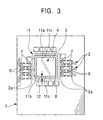
- Fig. 3 is a plan view of a major part of a high frequency unit according to a second embodiment of the present invention.
- a circuit substrate 1 formed of a laminated substrate and so forth has conductive patterns 2 formed in and on the surface of the laminated substrate, and the conductive patterns 2 have a large number of lands 2a disposed at desired places thereof.
- An IC component 4 including an outer package 3 composed of an insulating material is placed on the circuit substrate 1, and electrodes (not shown) disposed on the under surface of the IC component 4 are connected by soldering to the conductive patterns 2 via corresponding metal balls 5.
- the lands 2a are disposed around the IC component 4 so as to improve the density of the conductive patterns 2 and thus to achieve a reduced size.
- Electrical components 6 such as a chip-type capacitor and resistor are bonded and wired by using solder 7 to the corresponding lands 2a disposed close to and away from the IC component 4.
- a square-tube-shaped outflow preventive member 11 formed by molding an insulating material and serving as outflow preventive means has a wall 11a and a hollow 11b provided inside the wall 11a.
- the outflow preventive member 11 is fixed on the circuit substrate 1 by appropriate means in a state in which the IC component 4 is placed in the hollow 11b so as to provide a clearance 12 between the wall 11a and the IC component 4.
- thermosetting adhesive agent 8 composed of an epoxy resin or the like is filled in the clearance 12 provided between the circumference of the IC component 4 and the wall 11a so as to bond the IC component 4 to the circuit substrate 1, whereby the IC component 4 is prevented from becoming unstuck.
- the circuit substrate 1 is placed on a mother board 9 and is then incorporated into the mother board 9 by reflow-soldering.
- the solder 7 of the high frequency unit melts and expands; however, the solder 7 is not covered by the adhesive agent 8, whereby the expanded solder does not cause a problem of protruding out from the adhesive agent.
- the solder 7 does not cause a problem of short circuiting with the adjacent land 2a, and no short circuiting between the adjacent conductive patterns 2 occurs since no solder ball is produced.
- this outflow preventive means may be formed such that a solder resist layer or a silk layer is laminated on the circuit substrate so as to surround the circumference of the IC component.
- the adhesive agent is composed of a thermosetting resin in this embodiment; alternatively it may be composed of a thermoplastic resin.
- the outflow preventive member 11 has a plurality of space holders 11c, which protrude into the hollow 11b, formed on the wall 11a, and the space holders 11c abut against the IC component 4 so that the spacing between the wall 11a and the IC component 4 is kept so as to maintain the clearance 12, and also the space holders 11c are engaged with and held to the IC component 4 by sandwiching and holding the IC component from the four sides thereof) so that the outflow preventive member 11 is temporally fixed to the IC component 4.
- the space holders are disposed on the outflow preventive member in this embodiment, the space holders may be disposed on the IC component or on both the IC component and the outflow preventive member.
Landscapes
- Engineering & Computer Science (AREA)
- Microelectronics & Electronic Packaging (AREA)
- Manufacturing & Machinery (AREA)
- Electric Connection Of Electric Components To Printed Circuits (AREA)
- Structures Or Materials For Encapsulating Or Coating Semiconductor Devices Or Solid State Devices (AREA)
- Non-Metallic Protective Coatings For Printed Circuits (AREA)
Abstract
Description
Claims (5)
- A high frequency unit comprising: a circuit substrate including conductive patterns; an IC component placed on the circuit substrate; electrical components bonded by soldering to the conductive patterns disposed in the vicinity of the IC component; and outflow preventive means, for preventing an adhesive agent from flowing out, disposed on the circuit substrate so as to surround the circumference of the IC component, wherein the adhesive agent is filled in the spacing between the IC component and the outflow preventive means so as to bond the IC component to the circuit substrate.
- The high frequency unit according to Claim 1, wherein the adhesive agent comprises a thermosetting resin or a thermoplastic resin.
- The high frequency unit according to Claim 1 or 2, wherein the outflow preventive means is a tube-like outflow preventive member formed by molding an insulating material.
- The high frequency unit according to Claim 1, 2 or 3, wherein space holders are disposed on at least one of the outflow preventive member and the IC component so as to maintain the spacing between the IC component and the outflow preventive member.
- The high frequency unit according to Claim 4, wherein the outflow preventive member is engaged with and held to the IC component by disposing the space holders.
Applications Claiming Priority (2)
| Application Number | Priority Date | Filing Date | Title |
|---|---|---|---|
| JP2002037081 | 2002-02-14 | ||
| JP2002037081A JP2003243575A (en) | 2002-02-14 | 2002-02-14 | High frequency unit |
Publications (2)
| Publication Number | Publication Date |
|---|---|
| EP1337135A2 true EP1337135A2 (en) | 2003-08-20 |
| EP1337135A3 EP1337135A3 (en) | 2005-05-11 |
Family
ID=27621433
Family Applications (1)
| Application Number | Title | Priority Date | Filing Date |
|---|---|---|---|
| EP03250777A Withdrawn EP1337135A3 (en) | 2002-02-14 | 2003-02-07 | High frequency unit |
Country Status (3)
| Country | Link |
|---|---|
| EP (1) | EP1337135A3 (en) |
| JP (1) | JP2003243575A (en) |
| KR (1) | KR20030068458A (en) |
Cited By (1)
| Publication number | Priority date | Publication date | Assignee | Title |
|---|---|---|---|---|
| EP1722615A3 (en) * | 2005-05-10 | 2008-03-26 | Pace Micro Technology PLC | A printed circuit board having protection means and a method of use thereof |
Family Cites Families (5)
| Publication number | Priority date | Publication date | Assignee | Title |
|---|---|---|---|---|
| JPS6158248A (en) * | 1984-08-29 | 1986-03-25 | Toshiba Corp | Thin type semiconductor device |
| JPS61199642A (en) * | 1985-03-01 | 1986-09-04 | Fujitsu Ltd | Armoring method for hybrid integrated circuit |
| US5120678A (en) * | 1990-11-05 | 1992-06-09 | Motorola Inc. | Electrical component package comprising polymer-reinforced solder bump interconnection |
| JP2746234B2 (en) * | 1995-11-28 | 1998-05-06 | 日本電気株式会社 | Hybrid integrated circuit device and method of manufacturing the same |
| JP3241669B2 (en) * | 1998-11-09 | 2001-12-25 | 埼玉日本電気株式会社 | IC package reinforcement structure |
-
2002
- 2002-02-14 JP JP2002037081A patent/JP2003243575A/en not_active Withdrawn
-
2003
- 2003-02-07 EP EP03250777A patent/EP1337135A3/en not_active Withdrawn
- 2003-02-13 KR KR10-2003-0009006A patent/KR20030068458A/en not_active Ceased
Cited By (1)
| Publication number | Priority date | Publication date | Assignee | Title |
|---|---|---|---|---|
| EP1722615A3 (en) * | 2005-05-10 | 2008-03-26 | Pace Micro Technology PLC | A printed circuit board having protection means and a method of use thereof |
Also Published As
| Publication number | Publication date |
|---|---|
| JP2003243575A (en) | 2003-08-29 |
| KR20030068458A (en) | 2003-08-21 |
| EP1337135A3 (en) | 2005-05-11 |
Similar Documents
| Publication | Publication Date | Title |
|---|---|---|
| KR102380304B1 (en) | A printed circuit board comprising embeded electronic component within and a method for manufacturing | |
| US6272020B1 (en) | Structure for mounting a semiconductor device and a capacitor device on a substrate | |
| US4819041A (en) | Surface mounted integrated circuit chip package and method for making same | |
| JP4484176B2 (en) | Connection structure of ball grid array type package | |
| KR101123669B1 (en) | Circuit module | |
| US20060273461A1 (en) | Electronic device and method of manufacturing the same | |
| KR960042902A (en) | Printed circuit board with solder ball mounting groove and ball grid array package using the same | |
| US7400048B2 (en) | Void-free circuit board and semiconductor package having the same | |
| US20060281297A1 (en) | Multilayer electronic part and structure for mounting multilayer electronic part | |
| US7564121B2 (en) | Semiconductor device having shield structure | |
| JP5229401B2 (en) | Resin substrate with built-in electronic components and electronic circuit module | |
| US6101098A (en) | Structure and method for mounting an electric part | |
| JPH01256161A (en) | Printed wiring board device | |
| KR102117469B1 (en) | Electronic component module and manufacturing method threrof | |
| KR20150057788A (en) | Semi-conductor Package and Method for Manufacturing The same | |
| KR20150116605A (en) | Electric component module and manufacturing method threrof | |
| US20010040296A1 (en) | Printed-circuit board and method of mounting electric components thereon | |
| US5990421A (en) | Built in board resistors | |
| JP2016018928A (en) | Electronic component built-in module | |
| CN108695291A (en) | Electronic apparatus module and the method for manufacturing the electronic apparatus module | |
| JP2003046216A (en) | Mounting structure of surface mount electronic components, circuit boards and surface mount electronic components | |
| JP2002084070A (en) | Multilayer wiring board with built-in electronic components | |
| KR20150059086A (en) | Chip Embedded Board And Method Of Manufacturing The Same | |
| JP2003243575A (en) | High frequency unit | |
| JP2891254B2 (en) | Electronic components for surface mounting |
Legal Events
| Date | Code | Title | Description |
|---|---|---|---|
| PUAI | Public reference made under article 153(3) epc to a published international application that has entered the european phase |
Free format text: ORIGINAL CODE: 0009012 |
|
| AK | Designated contracting states |
Designated state(s): AT BE BG CH CY CZ DE DK EE ES FI FR GB GR HU IE IT LI LU MC NL PT SE SI SK TR |
|
| AX | Request for extension of the european patent |
Extension state: AL LT LV MK RO |
|
| PUAL | Search report despatched |
Free format text: ORIGINAL CODE: 0009013 |
|
| AK | Designated contracting states |
Kind code of ref document: A3 Designated state(s): AT BE BG CH CY CZ DE DK EE ES FI FR GB GR HU IE IT LI LU MC NL PT SE SI SK TR |
|
| AX | Request for extension of the european patent |
Extension state: AL LT LV MK RO |
|
| AKX | Designation fees paid |
Designated state(s): DE FI FR GB SE |
|
| STAA | Information on the status of an ep patent application or granted ep patent |
Free format text: STATUS: THE APPLICATION IS DEEMED TO BE WITHDRAWN |
|
| 18D | Application deemed to be withdrawn |
Effective date: 20051112 |