EP1335492A2 - Isolated gate drive circuit having a switched input capacitor - Google Patents
Isolated gate drive circuit having a switched input capacitor Download PDFInfo
- Publication number
- EP1335492A2 EP1335492A2 EP03075189A EP03075189A EP1335492A2 EP 1335492 A2 EP1335492 A2 EP 1335492A2 EP 03075189 A EP03075189 A EP 03075189A EP 03075189 A EP03075189 A EP 03075189A EP 1335492 A2 EP1335492 A2 EP 1335492A2
- Authority
- EP
- European Patent Office
- Prior art keywords
- capacitor
- drive circuit
- gate drive
- circuit
- input capacitor
- Prior art date
- Legal status (The legal status is an assumption and is not a legal conclusion. Google has not performed a legal analysis and makes no representation as to the accuracy of the status listed.)
- Withdrawn
Links
- 239000003990 capacitor Substances 0.000 title claims abstract description 63
- 238000002955 isolation Methods 0.000 claims abstract description 4
- 230000003213 activating effect Effects 0.000 claims 1
- 230000000295 complement effect Effects 0.000 description 3
- 238000010586 diagram Methods 0.000 description 3
- 238000012986 modification Methods 0.000 description 2
- 230000004048 modification Effects 0.000 description 2
- 239000004065 semiconductor Substances 0.000 description 2
- 230000015556 catabolic process Effects 0.000 description 1
- 238000009877 rendering Methods 0.000 description 1
Images

Classifications
-
- H—ELECTRICITY
- H03—ELECTRONIC CIRCUITRY
- H03K—PULSE TECHNIQUE
- H03K17/00—Electronic switching or gating, i.e. not by contact-making and –breaking
- H03K17/51—Electronic switching or gating, i.e. not by contact-making and –breaking characterised by the components used
- H03K17/56—Electronic switching or gating, i.e. not by contact-making and –breaking characterised by the components used by the use, as active elements, of semiconductor devices
- H03K17/687—Electronic switching or gating, i.e. not by contact-making and –breaking characterised by the components used by the use, as active elements, of semiconductor devices the devices being field-effect transistors
- H03K17/6871—Electronic switching or gating, i.e. not by contact-making and –breaking characterised by the components used by the use, as active elements, of semiconductor devices the devices being field-effect transistors the output circuit comprising more than one controlled field-effect transistor
- H03K17/6872—Electronic switching or gating, i.e. not by contact-making and –breaking characterised by the components used by the use, as active elements, of semiconductor devices the devices being field-effect transistors the output circuit comprising more than one controlled field-effect transistor using complementary field-effect transistors
-
- H—ELECTRICITY
- H03—ELECTRONIC CIRCUITRY
- H03K—PULSE TECHNIQUE
- H03K17/00—Electronic switching or gating, i.e. not by contact-making and –breaking
- H03K17/06—Modifications for ensuring a fully conducting state
- H03K17/063—Modifications for ensuring a fully conducting state in field-effect transistor switches
-
- H—ELECTRICITY
- H03—ELECTRONIC CIRCUITRY
- H03K—PULSE TECHNIQUE
- H03K17/00—Electronic switching or gating, i.e. not by contact-making and –breaking
- H03K17/51—Electronic switching or gating, i.e. not by contact-making and –breaking characterised by the components used
- H03K17/56—Electronic switching or gating, i.e. not by contact-making and –breaking characterised by the components used by the use, as active elements, of semiconductor devices
- H03K17/687—Electronic switching or gating, i.e. not by contact-making and –breaking characterised by the components used by the use, as active elements, of semiconductor devices the devices being field-effect transistors
- H03K17/6871—Electronic switching or gating, i.e. not by contact-making and –breaking characterised by the components used by the use, as active elements, of semiconductor devices the devices being field-effect transistors the output circuit comprising more than one controlled field-effect transistor
- H03K17/6874—Electronic switching or gating, i.e. not by contact-making and –breaking characterised by the components used by the use, as active elements, of semiconductor devices the devices being field-effect transistors the output circuit comprising more than one controlled field-effect transistor in a symmetrical configuration
-
- H—ELECTRICITY
- H03—ELECTRONIC CIRCUITRY
- H03K—PULSE TECHNIQUE
- H03K2217/00—Indexing scheme related to electronic switching or gating, i.e. not by contact-making or -breaking covered by H03K17/00
- H03K2217/0081—Power supply means, e.g. to the switch driver
Definitions
- This invention relates to a gate drive circuit for a MOS power transistor, and more particularly to a low cost gate drive circuit having an isolated output stage.
- MOSFETs MOS transistor switches
- IGBTs MOS transistor switches
- one terminal of the power supply is designated as the circuit common or ground
- transistors that couple the load to the circuit ground are referred to as low-side switches
- transistors that couple the load to the other terminal of the power supply are referred to as high-side switches.
- the emitter or source of a low-side transistor is referenced to circuit ground
- its gate drive circuit may also be referenced to ground, and a simple and inexpensive circuit design may be used.
- the emitter or source of a high-side transistor floats with respect to ground, and its gate drive circuit must therefore be isolated from ground. Drive circuit isolation may be accomplished in several different ways, but all are expensive, and the gate drive circuit frequently costs more than the power transistor it controls. Accordingly, what is needed is a simple and inexpensive isolated gate drive circuit.
- the present invention is directed to an improved low-cost gate drive circuit powered by a DC source voltage, the drive circuit having an isolated output stage with a parallel-connected by-pass capacitor and a switched input capacitor circuit that maintains a charge on the by-pass capacitor for driving the gate of a controlled MOS transistor while isolating the by-pass capacitor from the source voltage.
- a bank of controlled switches alternately couples the input capacitor to the source voltage and the by-pass capacitor, while in another embodiment, unidirectional isolation is achieved by replacing one or more of the controlled switches with diodes.
- the reference numeral 10 generally designates a gate drive circuit coupled across the gate (G) and source (S) terminals of a power MOSFET 12 (or alternately, an IGBT).
- the gate drive circuit 10 is powered by a DC source such as battery 14, the negative terminal of which is designated as circuit common or ground, as indicated by the reference numeral 16.
- the circuit application of MOSFET 12 is not important to the present invention, but it may be assumed for purposes of this disclosure that MOSFET 12 is configured as a high-side switch in a bridge circuit including a low-side MOSFET 18 that is referenced to the circuit ground or another voltage.
- the voltage potential at source (S) is not fixed, but instead varies depending on the conduction states of the MOSFETs 12 and 18.
- the gate drive circuit 10 includes an input capacitor 20, a by-pass capacitor 22, an output stage 24, and a capacitor switching arrangement 25 that is illustrated in Figure 1 as a double-pole double-throw (DPDT) switch 26.
- the output stage 24, which includes a pair of complementary transistors 28, 30, is coupled across the by-pass capacitor 22, with the node 32 between transistors 28 and 30 coupled to the gate (G) of MOSFET 12 via gate resistor 34 (which may be omitted, depending on the application).
- MOSFET 12 is an N-channel device, and its source (S) is coupled to the node 36 of by-pass capacitor 22; the source (S) of a P-channel device would be coupled to the opposite side of by-pass capacitor 22.
- the transistors 28 and 30 are controlled by a bridge control circuit, through the agency of a level shifting circuit 40 referenced to circuit ground 16.
- by-pass capacitor 22 is coupled across the gate (G) and source (S) terminals to bias MOSFET 12 conductive.
- transistor 30 When transistor 30 is conductive, it creates a low impedance path between the gate (G) and source (S) terminals to bias MOSFET 12 non-conductive.
- the input capacitor 20 is connected across the switch arms 26a, 26b, the terminals of battery 14 are connected across switch terminals 26c, 26d, and the by-pass capacitor 22 is connected across switch terminals 26e, 26f.
- the switch arms 26a, 26b are ganged, as indicated, under the control of an external switch control circuit 42.
- the DPDT switch 26 merely illustrates the functionality of the capacitor switching arrangement 25; in practice, the switching arrangement 25 is implemented with semiconductor switches, one such implementation being shown in Figure 2.
- the capacitor switching arrangement 25 comprises a set of four semiconductor switches 50, 52, 54, 56, each consisting of a pair of MOS switching transistors 50a, 50b; 52a, 52b; 54a, 54b; 56a, 56b controlled by oscillator (OSC) 58 through the agency of respective level shifting (LS) circuits 60, 62, 64, 66.
- the switches 50 and 52 couple the input capacitor 20 to the terminals of battery 14, while the switches 54 and 56 couple the input capacitor 20 to by-pass capacitor 22.
- Oscillator 58 performs the function of switch control circuit 42 by biasing switches 50, 52 and 54, 56 alternately conductive and non-conductive.
- the state of switch 26 illustrated in Figure 1 corresponds to an oscillator state in which switches 50 and 52 are conductive, and switches 54 and 56 are non-conductive, and vice versa for the opposite state of switch 26.
- the output stage transistors 28 and 30 are depicted as having individual level shifting circuits 68, 70, and as in Figure 1, each of the level shifting circuits 60, 62, 64, 66, 68, 70 are referenced to circuit ground 16.
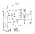
- Figure 3 depicts another embodiment of the gate drive circuit 10 that uni-directionally isolates the source (S) and gate (G) of MOSFET 12 from battery 14.
- This arrangement is suitable for applications where the drain (D) of MOSFET 12 is maintained at any potential up to the breakdown voltage of MOSFET 12, including voltages well in excess of battery 14, and simplifies the capacitor switching arrangement 25.
- the switches 50 and 54 of Figure 2 are replaced with diodes 80 and 84, respectively.
- the FET 82 carries out the function of switch 52
- MOSFET 86 carries out the function of switch 56.
- the oscillator 58 drives FET 82 via resistor 88, and drives MOSFET 86 via resistor 90 and a level shifting circuit comprising FET 92, pull-up resistor 94 and resistor 112.
- the battery 14 charges input capacitor 20 via diode 80 when FET 82 is biased conductive, and input capacitor 20 transfers its charge to by-pass capacitor 22 via diode 84 when MOSFET 86 is biased conductive.
- the output stage 24 is illustrated as comprising a first stage complementary transistor pair 96, 98 and a second stage complementary transistor pair 100, 102, both stages being connected in parallel with by-pass capacitor 22.
- a level shifting circuit comprising the FET 104 and resistors 106, 108 is coupled to the first stage transistors 96, 98, and is controlled by bridge control circuit 38 via resistor 110.
- the bridge control circuit 38 biases MOSFET 12 to a conductive state by biasing FET 104 off, thereby rendering output stage transistors 98 and 100 conductive to connect by-pass capacitor 22 across the gate (G) to source (S) circuit of MOSFET 12.
- the MOSFET 12 is biased to a non-conductive state by biasing FET 104 on, which renders transistors 96 and 102 conductive.
- a particularly advantageous aspect of the gate drive circuit 10 lies in its performance advantages, compared to other isolated gate driver topologies.
- the operating frequency and duty cycle of the output stage 24 may be very high (or very low) and are essentially independent of the capacitor switching arrangement 25.
- the charge transfer from input capacitor 20 to by-pass capacitor 22 occurs with high efficiency, typically in excess of 90%.
- gate drive circuit 10 is easily constructed as a single integrated circuit, with the exception of capacitors 20 and 22, which are implemented as external devices.
- the overall cost of a gate driver so constructed would be relatively low compared with other isolated gate driver topologies, and the circuit would exhibit the performance advantages described in the preceding paragraph.
- this invention provides a low-cost gate drive circuit having an isolated output stage with a parallel-connected by-pass capacitor and a switched input capacitor circuit that maintains a charge on the by-pass capacitor for driving the gate of a controlled device while uni-directionally or bidirectionally isolating the by-pass capacitor from the source voltage.
Landscapes
- Power Conversion In General (AREA)
- Electronic Switches (AREA)
- Amplifiers (AREA)
Abstract
Description
- This invention relates to a gate drive circuit for a MOS power transistor, and more particularly to a low cost gate drive circuit having an isolated output stage.
- Various circuits, including many power supply and motor control circuits, utilize one or more MOS transistor switches (MOSFETs or IGBTs) to selectively couple a load to a power supply. In general, one terminal of the power supply is designated as the circuit common or ground, and transistors that couple the load to the circuit ground are referred to as low-side switches, whereas transistors that couple the load to the other terminal of the power supply are referred to as high-side switches. Since the emitter or source of a low-side transistor is referenced to circuit ground, its gate drive circuit may also be referenced to ground, and a simple and inexpensive circuit design may be used. However, the emitter or source of a high-side transistor floats with respect to ground, and its gate drive circuit must therefore be isolated from ground. Drive circuit isolation may be accomplished in several different ways, but all are expensive, and the gate drive circuit frequently costs more than the power transistor it controls. Accordingly, what is needed is a simple and inexpensive isolated gate drive circuit.
- The present invention is directed to an improved low-cost gate drive circuit powered by a DC source voltage, the drive circuit having an isolated output stage with a parallel-connected by-pass capacitor and a switched input capacitor circuit that maintains a charge on the by-pass capacitor for driving the gate of a controlled MOS transistor while isolating the by-pass capacitor from the source voltage. In a fully isolated embodiment of the improved gate drive circuit, a bank of controlled switches alternately couples the input capacitor to the source voltage and the by-pass capacitor, while in another embodiment, unidirectional isolation is achieved by replacing one or more of the controlled switches with diodes.
-
- Figure 1 is a simplified circuit diagram of a fully isolated gate drive circuit according to this invention.
- Figure 2 is a more detailed circuit diagram of the fully isolated gate drive circuit of Figure 1.
- Figure 3 is a circuit diagram of a uni-directionally isolated gate drive circuit according to this invention.
-
- Referring to Figure 1, the
reference numeral 10 generally designates a gate drive circuit coupled across the gate (G) and source (S) terminals of a power MOSFET 12 (or alternately, an IGBT). Thegate drive circuit 10 is powered by a DC source such asbattery 14, the negative terminal of which is designated as circuit common or ground, as indicated by thereference numeral 16. The circuit application ofMOSFET 12 is not important to the present invention, but it may be assumed for purposes of this disclosure thatMOSFET 12 is configured as a high-side switch in a bridge circuit including a low-side MOSFET 18 that is referenced to the circuit ground or another voltage. Thus, the voltage potential at source (S) is not fixed, but instead varies depending on the conduction states of theMOSFETs - The
gate drive circuit 10 includes aninput capacitor 20, a by-pass capacitor 22, anoutput stage 24, and acapacitor switching arrangement 25 that is illustrated in Figure 1 as a double-pole double-throw (DPDT)switch 26. Theoutput stage 24, which includes a pair ofcomplementary transistors pass capacitor 22, with thenode 32 betweentransistors MOSFET 12 via gate resistor 34 (which may be omitted, depending on the application). In the illustrated embodiment,MOSFET 12 is an N-channel device, and its source (S) is coupled to thenode 36 of by-pass capacitor 22; the source (S) of a P-channel device would be coupled to the opposite side of by-pass capacitor 22. Thetransistors level shifting circuit 40 referenced tocircuit ground 16. Whentransistor 28 is conductive, by-pass capacitor 22 is coupled across the gate (G) and source (S) terminals to biasMOSFET 12 conductive. Whentransistor 30 is conductive, it creates a low impedance path between the gate (G) and source (S) terminals to biasMOSFET 12 non-conductive. Theinput capacitor 20 is connected across theswitch arms battery 14 are connected acrossswitch terminals pass capacitor 22 is connected acrossswitch terminals switch arms switch control circuit 42. - With the
switch arms input capacitor 20 is connected acrossbattery 14, while being electrically isolated from by-pass capacitor 22; in this state, theinput capacitor 20 is charged substantially to the battery terminal voltage. When theswitch arms input capacitor 20 is coupled in parallel with by-pass capacitor 22, while being electrically isolated frombattery 14; in this state, the charge ofinput capacitor 20 is transferred to by-pass capacitor 22. In operation, the state ofswitch 26 is periodically reversed byswitch control circuit 42 to transfer charge frombattery 14 to by-pass capacitor 22 viainput capacitor 20, while theoutput stage transistors bridge control circuit 38 to biasMOSFET 12 on and off. Thus, thebridge control circuit 38 and theswitch control circuit 42 may operate asynchronously. - As indicated above, the
DPDT switch 26 merely illustrates the functionality of thecapacitor switching arrangement 25; in practice, theswitching arrangement 25 is implemented with semiconductor switches, one such implementation being shown in Figure 2. Referring to Figure 2, thecapacitor switching arrangement 25 comprises a set of foursemiconductor switches MOS switching transistors circuits switches 50 and 52 couple theinput capacitor 20 to the terminals ofbattery 14, while theswitches 54 and 56 couple theinput capacitor 20 to by-pass capacitor 22.Oscillator 58 performs the function ofswitch control circuit 42 bybiasing switches switch 26 illustrated in Figure 1 corresponds to an oscillator state in whichswitches 50 and 52 are conductive, andswitches 54 and 56 are non-conductive, and vice versa for the opposite state ofswitch 26. In Figure 2, theoutput stage transistors level shifting circuits level shifting circuits circuit ground 16. - Figure 3 depicts another embodiment of the
gate drive circuit 10 that uni-directionally isolates the source (S) and gate (G) ofMOSFET 12 frombattery 14. This arrangement is suitable for applications where the drain (D) ofMOSFET 12 is maintained at any potential up to the breakdown voltage ofMOSFET 12, including voltages well in excess ofbattery 14, and simplifies thecapacitor switching arrangement 25. Specifically, the switches 50 and 54 of Figure 2 are replaced withdiodes switch 52, andMOSFET 86 carries out the function ofswitch 56. Theoscillator 58 drives FET 82 viaresistor 88, and drivesMOSFET 86 viaresistor 90 and a level shiftingcircuit comprising FET 92, pull-up resistor 94 andresistor 112. In operation, thebattery 14 chargesinput capacitor 20 viadiode 80 when FET 82 is biased conductive, andinput capacitor 20 transfers its charge to by-pass capacitor 22 viadiode 84 whenMOSFET 86 is biased conductive. Theoutput stage 24 is illustrated as comprising a first stagecomplementary transistor pair complementary transistor pair pass capacitor 22. A level shifting circuit comprising theFET 104 andresistors first stage transistors bridge control circuit 38 viaresistor 110. In operation, thebridge control circuit 38biases MOSFET 12 to a conductive state by biasingFET 104 off, thereby renderingoutput stage transistors pass capacitor 22 across the gate (G) to source (S) circuit ofMOSFET 12. TheMOSFET 12 is biased to a non-conductive state by biasingFET 104 on, which renderstransistors - A particularly advantageous aspect of the
gate drive circuit 10 lies in its performance advantages, compared to other isolated gate driver topologies. For example, the operating frequency and duty cycle of theoutput stage 24 may be very high (or very low) and are essentially independent of thecapacitor switching arrangement 25. Further, the charge transfer frominput capacitor 20 to by-pass capacitor 22 occurs with high efficiency, typically in excess of 90%. - Another advantageous aspect of the
gate drive circuit 10 is that it is easily constructed as a single integrated circuit, with the exception ofcapacitors - In summary, this invention provides a low-cost gate drive circuit having an isolated output stage with a parallel-connected by-pass capacitor and a switched input capacitor circuit that maintains a charge on the by-pass capacitor for driving the gate of a controlled device while uni-directionally or bidirectionally isolating the by-pass capacitor from the source voltage. While illustrated in reference to the illustrated embodiments, it is expected that various modifications will occur to persons skilled in the art, as indicated above. Accordingly, it should be understood that gate drive circuits incorporating such modifications may fall within the scope of this invention, which is defined by the appended claims.
Claims (5)
- A gate drive circuit (10) for a MOS power transistor (12) comprising:an output circuit (24) including an output capacitor (22) and an output switch (28, 30; 96, 98, 100, 102) controlled to selectively couple said output capacitor (22) to a gate terminal (G) of said MOS power transistor (12) for controlling a conduction state of said MOS power transistor (12);an input circuit including an input capacitor (20) and a voltage source (14); anda set of switching elements (25) controlled to alternately connect said input capacitor (20) to said voltage source (14) and to said output capacitor (22) so that said output capacitor (22) is charged from said voltage source (14) via said input capacitor (20) while maintaining isolation between said voltage source (14) and said output circuit (24).
- The gate drive circuit of Claim 1, wherein said set of switching elements (25) comprises:a first set of transistor switches (50, 52) effective when activated to connect said input capacitor (20) to said voltage source (14); anda second set of transistor switches (54, 56) effective when activated to connect said input capacitor (20) to said output capacitor (22).
- The gate drive circuit of Claim 2, including an oscillator (58) for alternately activating said first and second sets of transistor switches(50, 52; 54, 56).
- The gate drive circuit of Claim 1, wherein said set of switching elements (25) includes:a switching transistor (82) and diode (80) effective when said switching transistor (82) is activated to connect said input capacitor (20) to said voltage source (14).
- The gate drive circuit of Claim 1, wherein said set of switching elements (25) includes:a switching transistor (86) and diode (84) effective when said switching transistor (86) is activated to connect said input capacitor (20) to said output capacitor (22).
Applications Claiming Priority (2)
| Application Number | Priority Date | Filing Date | Title |
|---|---|---|---|
| US68454 | 2002-02-08 | ||
| US10/068,454 US6531895B1 (en) | 2002-02-08 | 2002-02-08 | Isolated gate drive circuit having a switched input capacitor |
Publications (2)
| Publication Number | Publication Date |
|---|---|
| EP1335492A2 true EP1335492A2 (en) | 2003-08-13 |
| EP1335492A3 EP1335492A3 (en) | 2006-07-05 |
Family
ID=22082671
Family Applications (1)
| Application Number | Title | Priority Date | Filing Date |
|---|---|---|---|
| EP03075189A Withdrawn EP1335492A3 (en) | 2002-02-08 | 2003-01-21 | Isolated gate drive circuit having a switched input capacitor |
Country Status (2)
| Country | Link |
|---|---|
| US (1) | US6531895B1 (en) |
| EP (1) | EP1335492A3 (en) |
Families Citing this family (14)
| Publication number | Priority date | Publication date | Assignee | Title |
|---|---|---|---|---|
| JP3788926B2 (en) * | 2001-10-19 | 2006-06-21 | 三菱電機株式会社 | Semiconductor device and transistor driving method |
| US6882212B2 (en) * | 2003-05-16 | 2005-04-19 | Power Integrations, Inc. | Method and apparatus for extending the size of a transistor beyond one integrated circuit |
| US7061301B2 (en) * | 2003-12-19 | 2006-06-13 | Power Integrations, Inc. | Method and apparatus switching a semiconductor switch with a multi-state drive circuit |
| US6975146B1 (en) | 2004-01-02 | 2005-12-13 | Sauer-Danfoss Inc. | High side NFET gate driving circuit |
| DE102004049817A1 (en) * | 2004-10-13 | 2006-04-27 | Semikron Elektronik Gmbh & Co. Kg | Integrated circuit arrangement for controlling power semiconductor switches |
| JP2009178926A (en) * | 2008-01-30 | 2009-08-13 | Seiko Epson Corp | Capacitive load drive circuit and liquid ejection device |
| JP5083546B2 (en) * | 2008-01-30 | 2012-11-28 | セイコーエプソン株式会社 | Capacitive load drive circuit and liquid ejection device |
| CA2759210A1 (en) | 2009-05-11 | 2010-11-18 | Ss Sc Ip, Llc | Gate driver for enhancement-mode and depletion-mode wide bandgap semiconductor jfets |
| US9806607B2 (en) * | 2014-09-10 | 2017-10-31 | Texas Instruments Incorporated | Circuit for controlling a power supply voltage for a high-side gate driver |
| US9525411B2 (en) * | 2014-11-13 | 2016-12-20 | Analog Devices, Inc. | Power supply circuits for gate drivers |
| US10622452B2 (en) * | 2018-06-05 | 2020-04-14 | Maxim Integrated Products, Inc. | Transistors with dual gate conductors, and associated methods |
| US11404960B2 (en) * | 2020-06-02 | 2022-08-02 | University Of Tennessee Research Foundation | Charge pump gate drive circuit for reduction in turn-on switching loss for MOSFETs |
| CN115276380B (en) * | 2022-07-15 | 2025-11-25 | 深圳陆巡科技有限公司 | An isolated drive circuit with multiple MOSFETs connected in parallel |
| CN120559324B (en) * | 2025-07-31 | 2025-10-24 | 南京大学 | Dynamic on-resistance test device and test method for wide bandgap semiconductor devices |
Citations (4)
| Publication number | Priority date | Publication date | Assignee | Title |
|---|---|---|---|---|
| US5103148A (en) | 1990-11-06 | 1992-04-07 | Motorola, Inc. | Low voltage circuit to control high voltage transistor |
| EP0723337A2 (en) | 1995-01-23 | 1996-07-24 | Sony Corporation | Switching circuit and composite arrangement |
| EP0855799A2 (en) * | 1997-01-28 | 1998-07-29 | Stribel GmbH | Control device |
| US5910746A (en) | 1993-03-26 | 1999-06-08 | Sundstrand Corporation | Gate drive for a power switching device |
Family Cites Families (6)
| Publication number | Priority date | Publication date | Assignee | Title |
|---|---|---|---|---|
| US4803612A (en) * | 1988-06-08 | 1989-02-07 | National Semiconductor Corporation | Clock ripple reduction in a linear low dropout C/DMOS regulator |
| US5055721A (en) * | 1989-04-13 | 1991-10-08 | Mitsubishi Denki Kabushiki Kaisha | Drive circuit for igbt device |
| US5359244A (en) * | 1992-07-31 | 1994-10-25 | Sgs-Thomson Microelectronics, Inc. | Gate drive circuit for a MOS power transistor |
| JP3517154B2 (en) * | 1998-04-30 | 2004-04-05 | 株式会社東芝 | Dielectric isolation integrated circuit |
| US6246296B1 (en) * | 1998-07-06 | 2001-06-12 | Kollmorgen Corporation | Pulse width modulator (PWM) with high duty cycle using bootstrap capacitor |
| US6459324B1 (en) * | 2000-10-23 | 2002-10-01 | International Rectifier Corporation | Gate drive circuit with feedback-controlled active resistance |
-
2002
- 2002-02-08 US US10/068,454 patent/US6531895B1/en not_active Expired - Fee Related
-
2003
- 2003-01-21 EP EP03075189A patent/EP1335492A3/en not_active Withdrawn
Patent Citations (5)
| Publication number | Priority date | Publication date | Assignee | Title |
|---|---|---|---|---|
| US5103148A (en) | 1990-11-06 | 1992-04-07 | Motorola, Inc. | Low voltage circuit to control high voltage transistor |
| US5910746A (en) | 1993-03-26 | 1999-06-08 | Sundstrand Corporation | Gate drive for a power switching device |
| EP0723337A2 (en) | 1995-01-23 | 1996-07-24 | Sony Corporation | Switching circuit and composite arrangement |
| EP0855799A2 (en) * | 1997-01-28 | 1998-07-29 | Stribel GmbH | Control device |
| US5977743A (en) | 1997-01-28 | 1999-11-02 | Stribel Gmbh | Control device |
Also Published As
| Publication number | Publication date |
|---|---|
| US6531895B1 (en) | 2003-03-11 |
| EP1335492A3 (en) | 2006-07-05 |
Similar Documents
| Publication | Publication Date | Title |
|---|---|---|
| US4736121A (en) | Charge pump circuit for driving N-channel MOS transistors | |
| US7692474B2 (en) | Control circuit for a high-side semiconductor switch for switching a supply voltage | |
| KR100720747B1 (en) | Bootstrap capacitor refresh circuit | |
| JP5354625B2 (en) | Semiconductor device | |
| US6531895B1 (en) | Isolated gate drive circuit having a switched input capacitor | |
| US7116153B2 (en) | Circuit for driving a depletion-type JFET | |
| US6172493B1 (en) | Switch-mode power converter circuit | |
| US7224204B2 (en) | Method and circuit for driving a gate of a MOS transistor negative | |
| WO2009002541A1 (en) | Gate driving scheme for depletion mode devices in buck converters | |
| KR20060053969A (en) | High Voltage Integrated Circuit Driver with High Voltage PMOS Bootstrap Diode Emulator | |
| JP3912417B2 (en) | Driving circuit | |
| US7911192B2 (en) | High voltage power regulation using two power switches with low voltage transistors | |
| US7893752B2 (en) | Charge pump circuit with control circuitry | |
| US20070013432A1 (en) | Semiconductor device and method of controlling the same | |
| KR20040029082A (en) | Half-bridge circuit | |
| CN110268631B (en) | Gate driver circuit for high-side switch | |
| CN104348339A (en) | Switch circuit arrangements and method for powering a driver circuit | |
| US6396333B2 (en) | Circuit for synchronous rectification with minimal reverse recovery losses | |
| JP7612201B2 (en) | Solenoid Drive Circuit | |
| CN115412002A (en) | Laser scanning motor drive circuit and laser radar scanning system | |
| KR102498234B1 (en) | Slew Control for High-Side Switches | |
| US12381558B2 (en) | Level shifter for high voltage driver | |
| GB2356504A (en) | A high side FET switch with a charge pump driven by a relatively low voltage CMOS inverter | |
| WO2024195419A1 (en) | Drive circuit for semiconductor element | |
| CN119727319A (en) | Output drive circuit for power devices |
Legal Events
| Date | Code | Title | Description |
|---|---|---|---|
| PUAI | Public reference made under article 153(3) epc to a published international application that has entered the european phase |
Free format text: ORIGINAL CODE: 0009012 |
|
| AK | Designated contracting states |
Designated state(s): AT BE BG CH CY CZ DE DK EE ES FI FR GB GR HU IE IT LI LU MC NL PT SE SI SK TR |
|
| AX | Request for extension of the european patent |
Extension state: AL LT LV MK RO |
|
| PUAL | Search report despatched |
Free format text: ORIGINAL CODE: 0009013 |
|
| AK | Designated contracting states |
Kind code of ref document: A3 Designated state(s): AT BE BG CH CY CZ DE DK EE ES FI FR GB GR HU IE IT LI LU MC NL PT SE SI SK TR |
|
| AX | Request for extension of the european patent |
Extension state: AL LT LV MK RO |
|
| 17P | Request for examination filed |
Effective date: 20070105 |
|
| AKX | Designation fees paid |
Designated state(s): DE FR GB |
|
| 17Q | First examination report despatched |
Effective date: 20070302 |
|
| STAA | Information on the status of an ep patent application or granted ep patent |
Free format text: STATUS: THE APPLICATION IS DEEMED TO BE WITHDRAWN |
|
| 18D | Application deemed to be withdrawn |
Effective date: 20101001 |