EP1335386A2 - Shift register - Google Patents
Shift register Download PDFInfo
- Publication number
- EP1335386A2 EP1335386A2 EP03002528A EP03002528A EP1335386A2 EP 1335386 A2 EP1335386 A2 EP 1335386A2 EP 03002528 A EP03002528 A EP 03002528A EP 03002528 A EP03002528 A EP 03002528A EP 1335386 A2 EP1335386 A2 EP 1335386A2
- Authority
- EP
- European Patent Office
- Prior art keywords
- data
- input
- bidirectional
- output
- bidirectional register
- Prior art date
- Legal status (The legal status is an assumption and is not a legal conclusion. Google has not performed a legal analysis and makes no representation as to the accuracy of the status listed.)
- Granted
Links
Images


Classifications
-
- G—PHYSICS
- G11—INFORMATION STORAGE
- G11C—STATIC STORES
- G11C19/00—Digital stores in which the information is moved stepwise, e.g. shift registers
- G11C19/28—Digital stores in which the information is moved stepwise, e.g. shift registers using semiconductor elements
-
- G—PHYSICS
- G11—INFORMATION STORAGE
- G11C—STATIC STORES
- G11C19/00—Digital stores in which the information is moved stepwise, e.g. shift registers
Definitions
- the present invention relates to a shift register formed by cascading a plurality of bidirectional register units and, more particularly, to a shift register which can quickly perform processing such as inserting and deleting data with respect to a held data string.
- JP-A- 2001-126491 reference 1
- JP-A- 2001-126491 reference 1
- the shift register disclosed in reference 1 can quickly and easily insert data into a data string, it requires a long processing time to delete specific data from a held data string. This is because, in order to delete specific data, data recorded on consecutive shift register units on the subsequent-stage of the shift register on which the data to be deleted is recorded must be sequentially read out, and the read data must be repeatedly written in the preceding-stage shift register units.
- a shift register comprising a plurality of bidirectional register units which are cascaded through first input/output terminals for data shifting and perform data shifting operation, the bidirectional register units having second input/output terminals which separately and directly input/output data, direction switching means for switching shifting directions of the bidirectional register units, register unit selection means for selecting one of the bidirectional register units and inputting/outputting data through the second input/output terminal, and shift clock supply means for supplying shift clocks to the bidirectional register units ranging from a bidirectional register unit selected by the register unit selection means to a last-stage bidirectional register unit.
- Fig. 1 shows a shift register according to the first embodiment of the present invention.
- the shift register according to this embodiment is comprised of n (n is a natural number equal to or more than 2) cascaded bidirectional register units (RUs) 11 to In and a shift control section 10 for controlling the bidirectional register units 11 to 1n.
- n is a natural number equal to or more than 2
- cascaded bidirectional register units (RUs) 11 to In and a shift control section 10 for controlling the bidirectional register units 11 to 1n.
- Each of the bidirectional register units 11 to In includes an m-bit (m is a natural number) input/output terminal (direct input/output terminal) A capable of parallelly inputting/outputting data from/to a data bus 9 having a m-bit bus width, an m-bit input/output terminal (preceding-stage shifting input/output terminal) B for parallelly inputting/outputting data to/from the preceding-stage bidirectional register unit, and an m-bit input/output terminal (subsequent-stage shifting input/output terminal) C for parallelly inputting/outputting data to/from the subsequent-stage bidirectional register unit.
- m-bit m is a natural number
- Each of the bidirectional register units 11 to 1n also includes a CLK signal terminal for inputting a CLK signal (shift clock), a DIR signal terminal for inputting a DIR signal for designating a shifting direction, an SEL signal terminal for inputting an SEL signal for designating a bidirectional register unit which directly inputs/outputs data to/from the data bus 9, and an OE signal terminal for inputting an OE signal for causing the register unit to output held data to the data bus 9, together with the SEL signal.
- CLK signal terminal for inputting a CLK signal (shift clock)
- DIR signal terminal for inputting a DIR signal for designating a shifting direction
- an SEL signal terminal for inputting an SEL signal for designating a bidirectional register unit which directly inputs/outputs data to/from the data bus 9
- an OE signal terminal for inputting an OE signal for causing the register unit to output held data to the data bus 9, together with the SEL signal.
- the shifting direction of each of the bidirectional register units 11 to 1n can be changed by the DIR signal. Assume that the shifting direction from left to right is the forward direction, and the shifting direction from right to left is the reverse direction.
- each of the bidirectional register units 11 to 1n outputs held data from the input/output terminal C.
- the output data output from the input/output terminal C of the preceding-stage bidirectional register unit or data on the data bus 9 is selected as input data in accordance with the SEL signal.
- the input data is received in response to the CLK signal.
- each of the bidirectional register units 11 to 1n selects the input/output terminal A or input/output terminal B as a terminal for receiving the input data in accordance with the SEL signal.
- the received input data is held until the next CLK signal is input.
- the input/output terminal A has been selected in accordance with the SEL signal and the OE signal is input to the OE signal terminal, the held data is output to the data bus 9.
- the OE signal is externally supplied as a common signal to the bidirectional register units 11 to 1n.
- each of the bidirectional register units 11 to 1n When the DIR signal is set in the reverse direction, each of the bidirectional register units 11 to 1n outputs held data from the input/output terminal B. Each bidirectional register unit receives the output data from the input/output terminal B of the subsequent-stage bidirectional register unit as input data in response to the CLK signal, and holds the data until the next CLK signal is input.
- the input/output terminal A has been selected in accordance with the SEL signal and the OE signal is input to the OE signal terminal, the held data is output to the data bus 9.
- the shift control section 10 has k-bit (k is a natural number) RU number designation terminals, a DIR signal input terminal, a CLK signal input terminal, and n sets of SEL signal output terminals, DIR signal output terminals, and CLK signal output terminals which exhibit one-to-one correspondence with the bidirectional register units 11 to 1n.
- the DIR input terminals and DIR output terminals constitute shifting direction switching means.
- the shift control section 10 includes the bidirectional register unit selection means for selectively performing data input/output operation with respect to arbitrary bidirectional register units through the direct input/output terminals, the shift clock supply means for selectively supplying shift clocks to the cascaded bidirectional register units 11 to 1n ranging from the bidirectional register unit selected by the bidirectional register unit selection means to the last bidirectional register unit, and the input/output direction switching means for switching input/output directions of the respective bidirectional register units 11 to 1n.
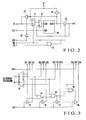
- Fig. 2 shows a 1-bit arrangement of each bidirectional register unit. Such circuits are arranged in parallel by the bus width of the data bus to constitute each of the bidirectional register units 11 to 1n.
- the 1-bit circuit shown in Fig. 2 is comprised of a D-type flip-flop 20, selectors 21 and 22, enabled buffers 23, 24, and 25, a NOT circuit 26, and an AND circuit 27.
- the D-type flip-flop 20 has a data input terminal DIN, data output terminal DOUT, and a CLK signal input terminal CLK.
- the data input terminal DIN is connected to the output terminal of the selector 22 which is used to switch input operations in the forward and reverse directions.
- the data output terminal DOUT is connected to the input of each of the enabled buffers 23, 24, and 25.
- the CLK signal input terminal CLK is connected to the CLK signal terminal of the bidirectional register unit.
- a latch or the like may be used in place of the D-type flip-flop 20.
- a reset or preset signal is generally connected to the D-type flip-flop, a description thereof will be omitted for the sake of simplicity.
- Each of the selectors 21 and 22 has two input terminals "0" and “1", a selection signal input terminal, and an output terminal.
- the input terminal "0” is connected to an input/output terminal Bi (1 ⁇ i ⁇ m) of the bidirectional register unit
- the input terminal "1” is connected to an input/output terminal Ai (1 ⁇ i ⁇ m) of the bidirectional register unit
- the selection signal input terminal is connected to the SEL signal terminal of the bidirectional register unit.
- the input terminal "0" is connected to an input/output terminal Ci (1 ⁇ i ⁇ m) of the bidirectional register unit
- the input terminal "1" is connected to the output terminal of the bidirectional interface 21
- the selection signal input terminal is connected to the DIR signal terminal of the bidirectional register unit
- the output terminal is connected to the data input terminal DIN of the D-type flip-flop 20.
- Each of the enabled buffers 23, 24, and 25 has an input terminal, enable signal input terminal, and output terminal.
- the input terminal is connected to the data output terminal DOUT of the D-type flip-flop 20 as described above, the output terminal is connected to the input/output terminal Bi (1 ⁇ i ⁇ m) of the bidirectional register unit, and the enable signal input terminal is connected to the output terminal of the NOT circuit 26.
- the input terminal of the NOT circuit 26 is connected to the DIR signal terminal of the bidirectional register unit.
- the input terminal is connected to the data output terminal DOUT of the D-type flip-flop 20 as described above, the output terminal is connected to the input/output terminal Ai (1 ⁇ i ⁇ m) of the bidirectional register unit, and the enable signal input terminal is connected to the output terminal of the AND circuit 27.
- the AND circuit 27 has two input terminals. One of these input terminals is connected to the SEL signal terminal of the bidirectional register unit, and the other input terminal is connected to the OE signal terminal.
- the input terminal is connected to the data output terminal DOUT of the D-type flip-flop 20 as described above, the output terminal is connected to the input/output terminal Ci (1 ⁇ i ⁇ m) of the bidirectional register unit, and the enable signal input terminal is connected to the DIR signal terminal of the bidirectional register unit.
- each 1-bit circuit having the above arrangement will be described next.
- the bidirectional register unit performs operation in the forward direction.
- the input/output terminal Bi and input/output terminal Ci respectively serve as a data input port and data output port owing to the functions of the selector 22, enabled buffers 23 and 25, and NOT circuit 26.
- the selector 21 selects the input/output terminal Bi to which a signal from the preceding-stage bidirectional register unit is input.
- the selector 21 selects the input/output terminal Ai to which a signal from the data bus is input. In response to the CLK signal, the selected input data is received.
- the input/output terminal Ci and input/output terminal Bi of the bidirectional register unit serve as a data input port and data output port, respectively, thereby performing reverse shifting operation. That is, the input data from the input/output terminal Ci is received in response to the CLK signal.
- the AND circuit 27 is set at "H” level regardless of the direction of the DIR signal, and the enabled buffer 24 is rendered conductive, thereby outputting data from the D-type flip-flop 20 onto the data bus.
- Fig. 3 shows the detailed arrangement of the shift control section 10.
- the circuit shown in Fig. 3 is comprised of a line decoder 30, n enabled buffers 31 to 3n, and (n - 1) OR circuits 42 to 4n.
- the line decoder (register unit selection means) 30 has RU number designation signal input terminals 1 to k connected to k-bit (k is a natural number) RU number designation terminals of the shift control section 10 in one-to-one correspondence, and n output terminals 1 to n for outputting input signal decoding results.
- Each of the enabled buffers (shift clock supply means) 31 to 3n has an input terminal, enable signal input terminal, and output terminal.
- Each of the OR circuits 42 to 4n has two input terminals and an output terminal.
- the n output terminals 1 to n of the line decoder 30 are connected to the n SEL signal outputs of the shift control section in one-to-once correspondence.
- the output terminal 1 is connected to the enable signal input terminal of the first-stage enabled buffer 31 and one input terminal of the second-stage OR circuit 42.
- the output terminal 2 of the line decoder 30 is connected to the other input terminal of the OR circuit 42.
- the output terminal of the OR circuit 42 is connected to the enable signal input terminal of the second-stage enabled buffer 32 and one input terminal of the third-stage OR circuit 43.
- the output terminals of the OR circuits 43 to 4n are connected to the enable signal input terminals of the enabled buffers 33 to 3n on the same stages, and the output terminal of each of the OR circuits 43 to 4(n-1) is connected to one input terminal of the subsequent-stage OR circuit.
- Each of the output terminals 3 to n of the line decoder 30 is connected to the other input terminal of a corresponding one of the OR circuits 43 to 4n.
- the DIR signal input terminal of the shift control section is connected to the n DIR signal output terminals of the shift control section.
- the DIR signal is transferred to all the DIR signal output terminals without any special processing.
- the embodiment may additionally have a circuit for performing control to change the polarities of only DIR signals following a DIR signal corresponding to the number designated by the SEL signal as in the case of the CLK signal.
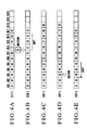
- Step 1 indicates a data string stored in the bidirectional registers RU1 to RU14 at a given time point.
- step 2 when data B4 is generated, the data B4 should be inserted between the data B3 and the data C1.
- the data B4 is output onto the data bus first.
- RU number designation data indicating the eighth-stage bidirectional register unit RU8 in which the data C1 is stored is input to the RU number designation terminals of the shift control section 10.
- the DIR signal set in the forward direction is input to the DIR signal input terminal.
- the CLK signal as a shift clock is applied to the CLK signal input terminal of the shift control section 10.
- Step 3 (Fig. 4C) indicates the result of the above inserting operation.
- data can be easily and quickly inserted at an arbitrary position to construct a data string with a desired arrangement.
- Step 5 indicates the result of the above deleting operation. According to this embodiment, deletion of data at an arbitrary position and filling operation can be easily and quickly done to construct a data string with a desired arrangement.
- RU number designation data indicating the bidirectional register unit in which the data to be read out is stored may be input to the RU number designation terminals of the shift control section 10, together with the OE signal. With this operation, the data held in the designated bidirectional register unit is output to the data bus 9. This makes it possible to externally read out the data.
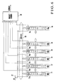
- Fig. 5 shows a shift register according to the second embodiment of the present invention.
- the position of the data B3 must be detected to insert the data B4, and the position of the data A3 must be detected to delete the data A3.
- the first method is available, which searches for data one by one from the start.
- the second method using dichotomy is also available, which is executed as follows. If the arrangement of data exhibits regularity, an intermediate value is found, and it is checked whether the target value is located before or after the intermediate value. In the remaining half group, the location of the target value is determined from an intermediate value in the same manner, thereby narrowing the search. In either of the methods, a considerably large number of steps are required on average until the target value is detected.
- FIG. 5 shows elements added to the shift register described with reference to Fig. 1. An illustration of a shift control section 10 is omitted.
- bidirectional register units 51 to 5n as RU1 to RUn are identical to the bidirectional register units 11 to 1n in Fig. 1.
- Input terminals A of the comparators 61 to 6n are connected to a data bus 60, and input terminals B are connected to the output terminals of the flip-flops (or latches) of the bidirectional register units 51 to 5n on the same stages.
- Coincidence detection outputs from the respective comparators 61 to 6n are input to the priority encoder 50, and numbers 1 to n of outputs which are set at "H" level as a result of coincidence detection are encoded into binary data or the like.
- the resultant data is output as address information. If a plurality of data exhibit coincidence, the priority encoder 50 outputs, for example, the smallest or largest number. If no data exhibits coincidence, incoincidence detection data is set at "H" level. That is, in this embodiment, a number corresponding to a bidirectional register unit in which data is stored is output by the n comparators 61 to 6n and priority encoder 50 in accordance with the designation of the stored data content. Note that this embodiment also has a function of excluding (masking) data from comparison targets in comparing operation of each comparator.
- the comparator at the position corresponding to the data B3 is set at "H" level by only setting the data B3 on the data bus 60, and the address information of the location can be quickly recognized.
- the line decoder 30 selects one of the bidirectional register units, which is used to insert or delete data, in accordance with the obtained address information.
- Fig. 6 shows a shift register according to the third embodiment of the present invention.
- This embodiment differs from the first embodiment in that one bit of each of bidirectional register units 71 to 7n is assigned as an end detection bit, latches 71a to 7na storing the end detection bits are connected to a pull-up signal line 81 through input/output terminals A, and the output terminals of the latches 71a to 7na are connected to input terminals 1 to n of a priority encoder 70.
- the latches 71a to 7na and priority encoder 70 constitute an address output means.
- All the end detection bits are reset to "L" level in the initial state.
- the "H"-level end detection bit is set in a corresponding one of the latches 71a to 7na. Since this bit information is transferred to the next stage by shifting operation, the end detection bits in all bidirectional register units in which data are set are set at "H" level, while those in the remaining bidirectional register units are set at "L” level. Since the end detection bit is also output to the priority encoder 70, the smallest number of the "H"-level input is encoded into binary data or the like by the priority encoder 70. This data is output as address information.
- the 1-bit bidirectional registers assigned to the respective bidirectional register units 71 to 7n constitute a bidirectional register for inputting/outputting end detection information
- the priority encoder 70 outputs a number corresponding to the bidirectional register unit in which the end detection information is stored.
- each bidirectional register unit is constituted by a plurality of bidirectional registers, and shift clocks are synchronously applied to these bidirectional registers.
- input/output operations through the input/output terminals of the respective bidirectional registers are synchronously done. Therefore, data can be easily and quickly inserted and deleted on a byte or word basis not only when serial data is used as a data string but also when byte data or word data is used.
- the present invention further includes the means for, when a stored data content is designated, outputting a number corresponding to the bidirectional register unit in which the data is stored, a bidirectional register unit in or from which data should be inserted or deleted can be easily and quickly detected.
- each bidirectional register unit further has the bidirectional register which inputs/outputs end detection information
- the present invention further includes the means for outputting a number corresponding to a bidirectional register unit in which end detection information is stored, the end of a stored data string can be easily and quickly detected.
- a means such as a memory on which information indicating up to which bidirectional register unit data has been stored is recoded, the arrangement of the shift register is simplified, and a reduction in cost can be achieved.
Landscapes
- Shift Register Type Memory (AREA)
- Logic Circuits (AREA)
Abstract
Description
Claims (8)
- A shift register characterized by comprising:a plurality of bidirectional register units (11 - 1n) which are cascaded through first input/output terminals (B, C) for data shifting and perform data shifting operation, said bidirectional register units having second input/output terminals (A) which separately and directly input/output data;direction switching means (DIR) for switching shifting directions of said bidirectional register units;register unit selection means (30) for selecting one of said bidirectional register units and inputting/outputting data through the second input/output terminal; andshift clock supply means (31 - 3n) for supplying shift clocks to said bidirectional register units ranging from a bidirectional register unit selected by said register unit selection means to a last-stage bidirectional register unit.
- A register according to claim 1, wherein the first and second input/output terminals of said bidirectional register unit parallelly input/output data constituted by a plurality of bits.
- A register according to claim 1 or 2, wherein
each of said bidirectional register units comprises a plurality of latch circuits arranged in parallel in correspondence with data constituted by a plurality of bits, and
shift clocks from said shift clock supply means are synchronously applied to the plurality of latch circuits, and input/output operations of the latch circuits are synchronously performed through direct input/output terminals. - A register according to claim 1, 2, or 3 further comprising address output means (61 - 6n, 50) for designating a data content stored in one of said bidirectional register units to output an address indicating a bidirectional register unit corresponding to the designated data content.
- A register according to claim 4, wherein said address output means comprises:a plurality of comparators (61 - 6n) which are respectively provided for said bidirectional register units and compare comparative data with data stored in said bidirectional register units; andan encoder (50) which receives comparison outputs from said respective comparators and outputs an address of a bidirectional register unit having stored data identical to the comparative data.
- A register according to claim 5, wherein said register unit selection means selects said bidirectional register unit in accordance with the address output from said encoder, and performs one of deletion and shifting operation of data stored in said selected register unit.
- A register according to any one of claims 1 to 6, furthe comprising address output means (71a - 7na, 70) for outputting an address of said bidirectional register unit in which data is inserted last in accordance with outputting of end detection information stored in said bidirectional register unit at the time of data insertion through a direct input/output terminal.
- A register according to any one of claims 1 to 7, wherein said address output means comprises:a plurality of latch circuits (71a - 7na) which are respectively provided for said bidirectional register units and in which end detection information is stored in accordance with data inserting operation; andan encoder (70) which receives latch outputs from the respective latch circuits and outputs an address of said bidirectional register unit in which data is inserted last.
Applications Claiming Priority (2)
| Application Number | Priority Date | Filing Date | Title |
|---|---|---|---|
| JP2002029070A JP3765273B2 (en) | 2002-02-06 | 2002-02-06 | Shift register |
| JP2002029070 | 2002-02-06 |
Publications (3)
| Publication Number | Publication Date |
|---|---|
| EP1335386A2 true EP1335386A2 (en) | 2003-08-13 |
| EP1335386A3 EP1335386A3 (en) | 2005-03-09 |
| EP1335386B1 EP1335386B1 (en) | 2007-04-11 |
Family
ID=27606486
Family Applications (1)
| Application Number | Title | Priority Date | Filing Date |
|---|---|---|---|
| EP03002528A Expired - Lifetime EP1335386B1 (en) | 2002-02-06 | 2003-02-05 | Shift register |
Country Status (4)
| Country | Link |
|---|---|
| US (1) | US6904116B2 (en) |
| EP (1) | EP1335386B1 (en) |
| JP (1) | JP3765273B2 (en) |
| DE (1) | DE60313059T2 (en) |
Families Citing this family (10)
| Publication number | Priority date | Publication date | Assignee | Title |
|---|---|---|---|---|
| JP2003037572A (en) | 2001-07-23 | 2003-02-07 | Nec Corp | Scheduling method |
| EP2727114B1 (en) | 2011-06-28 | 2020-04-22 | Hewlett-Packard Enterprise Development LP | Shiftable memory |
| EP2771885B1 (en) | 2011-10-27 | 2021-12-01 | Valtrus Innovations Limited | Shiftable memory supporting atomic operation |
| DE112011105670B4 (en) * | 2011-10-27 | 2020-10-08 | Hewlett Packard Enterprise Development Lp | Movable memory using ring registers |
| KR101660611B1 (en) | 2012-01-30 | 2016-09-27 | 휴렛 팩커드 엔터프라이즈 디벨롭먼트 엘피 | Word shift static random access memory(ws-sram) |
| WO2013130109A1 (en) | 2012-03-02 | 2013-09-06 | Hewlett-Packard Development Company L.P. | Shiftable memory defragmentation |
| US20150318054A1 (en) * | 2012-12-11 | 2015-11-05 | Hewlett-Packard Development Company, L.P. | Data Operation in Shift Register Ring |
| US10049707B2 (en) | 2016-06-03 | 2018-08-14 | Micron Technology, Inc. | Shifting data |
| CN110867153B (en) * | 2018-08-28 | 2023-03-14 | 瑞鼎科技股份有限公司 | Source electrode driving circuit and shift register thereof |
| CN120014965B (en) * | 2025-03-14 | 2026-04-17 | 松励微电子(上海)有限公司 | A method, circuit, and device for interrupted transmission of LEDs with dual input and dual output. |
Family Cites Families (18)
| Publication number | Priority date | Publication date | Assignee | Title |
|---|---|---|---|---|
| US4387341A (en) * | 1981-05-13 | 1983-06-07 | Rca Corporation | Multi-purpose retimer driver |
| JPS63160408A (en) | 1986-12-24 | 1988-07-04 | Oki Electric Ind Co Ltd | Two-way delay flip-flop circuit |
| JP2545478B2 (en) | 1990-01-29 | 1996-10-16 | 富士通株式会社 | Start bit detection circuit |
| US5632748A (en) * | 1993-06-14 | 1997-05-27 | Linvatec Corporation | Endosteal anchoring device for urging a ligament against a bone surface |
| US5522843A (en) * | 1994-02-23 | 1996-06-04 | Orthopaedic Biosystems Limited, Inc. | Apparatus for attaching soft tissue to bone |
| US5603716A (en) * | 1995-02-16 | 1997-02-18 | Arthrex Inc. | Method of ligament reconstruction using double socket graft placement and fixation |
| US5643320A (en) * | 1995-03-13 | 1997-07-01 | Depuy Inc. | Soft tissue anchor and method |
| US5662658A (en) * | 1996-01-19 | 1997-09-02 | Mitek Surgical Products, Inc. | Bone anchor inserter, method for loading same, method for holding and delivering a bone anchor, and method for inserting a bone anchor in a bone |
| US6319270B1 (en) * | 1996-08-05 | 2001-11-20 | Arthrex, Inc. | Headed bioabsorbable tissue anchor |
| US5733307A (en) * | 1996-09-17 | 1998-03-31 | Amei Technologies, Inc. | Bone anchor having a suture trough |
| SE9701874D0 (en) | 1997-05-21 | 1997-05-21 | Ferenc Belik | Address adjustable RAM memory (or shift memory) |
| US5968045A (en) * | 1997-10-14 | 1999-10-19 | Frazier; John K. | Intra-articular tendon sling fixation screw |
| US5871504A (en) * | 1997-10-21 | 1999-02-16 | Eaton; Katulle Koco | Anchor assembly and method for securing ligaments to bone |
| US5964783A (en) * | 1997-11-07 | 1999-10-12 | Arthrex, Inc. | Suture anchor with insert-molded suture |
| US6102934A (en) * | 1998-06-02 | 2000-08-15 | Li; Lehmann K. | Anchor tool and method and apparatus for emplacing anchor in a borehole |
| US6355066B1 (en) * | 1998-08-19 | 2002-03-12 | Andrew C. Kim | Anterior cruciate ligament reconstruction hamstring tendon fixation system |
| JP3744285B2 (en) | 1999-10-29 | 2006-02-08 | 日本電気株式会社 | Shift register and control method thereof |
| US6641597B2 (en) * | 2001-05-25 | 2003-11-04 | Arthrex, Inc. | Interference fit knotless suture anchor fixation |
-
2002
- 2002-02-06 JP JP2002029070A patent/JP3765273B2/en not_active Expired - Fee Related
-
2003
- 2003-02-05 US US10/358,198 patent/US6904116B2/en not_active Expired - Fee Related
- 2003-02-05 DE DE60313059T patent/DE60313059T2/en not_active Expired - Lifetime
- 2003-02-05 EP EP03002528A patent/EP1335386B1/en not_active Expired - Lifetime
Also Published As
| Publication number | Publication date |
|---|---|
| EP1335386A3 (en) | 2005-03-09 |
| US6904116B2 (en) | 2005-06-07 |
| DE60313059T2 (en) | 2007-08-16 |
| EP1335386B1 (en) | 2007-04-11 |
| DE60313059D1 (en) | 2007-05-24 |
| JP2003228990A (en) | 2003-08-15 |
| US20030147488A1 (en) | 2003-08-07 |
| JP3765273B2 (en) | 2006-04-12 |
Similar Documents
| Publication | Publication Date | Title |
|---|---|---|
| US6401148B1 (en) | FIFO memory system and method with improved determination of amount of data stored using a binary read address synchronized to a write clock | |
| JP3285354B2 (en) | Maximum value search circuit | |
| EP0047440A1 (en) | Shift circuit | |
| KR100238931B1 (en) | Fail Analysis Device of Semiconductor Memory Test Device | |
| EP1335386B1 (en) | Shift register | |
| US4524345A (en) | Serial comparison flag detector | |
| US4945518A (en) | Line memory for speed conversion | |
| CN101458967B (en) | Bidirectional shift register | |
| EP1096506B1 (en) | Shift register allowing direct data insertion | |
| US20190385683A1 (en) | Semiconductor device | |
| US6898722B2 (en) | Parallel data transfer method and system of DDR divided data with associated transfer clock signal over three signal lines | |
| EP1612662A2 (en) | Address generator and arithmetic circuit | |
| US6836525B1 (en) | Method for establishing a gray code and related counter circuit | |
| JPH0666050B2 (en) | Sort processing method | |
| RU2658147C1 (en) | Data decompression device | |
| EP0843253B1 (en) | A method for reducing the number of bits needed for the representation of constant values in a data processing device | |
| WO2000010089A1 (en) | Content addressable memory addressable by redundant form input data | |
| US6397272B1 (en) | Interruption processing circuit for receiving and storing data associated with an event | |
| US3678476A (en) | Read-only random access serial memory systems | |
| KR100205351B1 (en) | Address sorter of semiconductor memory | |
| KR20000013941A (en) | High-speed empty flag generator | |
| US20030056080A1 (en) | Register read circuit using the remainders of modulo of a register number by the number of register sub-banks | |
| JP6842098B1 (en) | Debugging device and debugging method | |
| RU2222822C2 (en) | Device for programmed control over electric motor drives, electron keys and signaling | |
| JP2005267415A (en) | Sequence control circuit |
Legal Events
| Date | Code | Title | Description |
|---|---|---|---|
| PUAI | Public reference made under article 153(3) epc to a published international application that has entered the european phase |
Free format text: ORIGINAL CODE: 0009012 |
|
| AK | Designated contracting states |
Designated state(s): AT BE BG CH CY CZ DE DK EE ES FI FR GB GR HU IE IT LI LU MC NL PT SE SI SK TR |
|
| AX | Request for extension of the european patent |
Extension state: AL LT LV MK RO |
|
| PUAL | Search report despatched |
Free format text: ORIGINAL CODE: 0009013 |
|
| AK | Designated contracting states |
Kind code of ref document: A3 Designated state(s): AT BE BG CH CY CZ DE DK EE ES FI FR GB GR HU IE IT LI LU MC NL PT SE SI SK TR |
|
| AX | Request for extension of the european patent |
Extension state: AL LT LV MK RO |
|
| 17P | Request for examination filed |
Effective date: 20050207 |
|
| 17Q | First examination report despatched |
Effective date: 20050418 |
|
| AKX | Designation fees paid |
Designated state(s): DE FI GB SE |
|
| GRAP | Despatch of communication of intention to grant a patent |
Free format text: ORIGINAL CODE: EPIDOSNIGR1 |
|
| GRAS | Grant fee paid |
Free format text: ORIGINAL CODE: EPIDOSNIGR3 |
|
| GRAA | (expected) grant |
Free format text: ORIGINAL CODE: 0009210 |
|
| AK | Designated contracting states |
Kind code of ref document: B1 Designated state(s): DE FI GB SE |
|
| REG | Reference to a national code |
Ref country code: GB Ref legal event code: FG4D |
|
| REF | Corresponds to: |
Ref document number: 60313059 Country of ref document: DE Date of ref document: 20070524 Kind code of ref document: P |
|
| REG | Reference to a national code |
Ref country code: SE Ref legal event code: TRGR |
|
| PLBE | No opposition filed within time limit |
Free format text: ORIGINAL CODE: 0009261 |
|
| STAA | Information on the status of an ep patent application or granted ep patent |
Free format text: STATUS: NO OPPOSITION FILED WITHIN TIME LIMIT |
|
| 26N | No opposition filed |
Effective date: 20080114 |
|
| PGFP | Annual fee paid to national office [announced via postgrant information from national office to epo] |
Ref country code: DE Payment date: 20160202 Year of fee payment: 14 |
|
| PGFP | Annual fee paid to national office [announced via postgrant information from national office to epo] |
Ref country code: SE Payment date: 20160211 Year of fee payment: 14 Ref country code: FI Payment date: 20160209 Year of fee payment: 14 Ref country code: GB Payment date: 20160203 Year of fee payment: 14 |
|
| REG | Reference to a national code |
Ref country code: DE Ref legal event code: R119 Ref document number: 60313059 Country of ref document: DE |
|
| REG | Reference to a national code |
Ref country code: SE Ref legal event code: EUG |
|
| GBPC | Gb: european patent ceased through non-payment of renewal fee |
Effective date: 20170205 |
|
| PG25 | Lapsed in a contracting state [announced via postgrant information from national office to epo] |
Ref country code: FI Free format text: LAPSE BECAUSE OF NON-PAYMENT OF DUE FEES Effective date: 20170205 |
|
| PG25 | Lapsed in a contracting state [announced via postgrant information from national office to epo] |
Ref country code: SE Free format text: LAPSE BECAUSE OF NON-PAYMENT OF DUE FEES Effective date: 20170206 |
|
| PG25 | Lapsed in a contracting state [announced via postgrant information from national office to epo] |
Ref country code: DE Free format text: LAPSE BECAUSE OF NON-PAYMENT OF DUE FEES Effective date: 20170901 |
|
| PG25 | Lapsed in a contracting state [announced via postgrant information from national office to epo] |
Ref country code: GB Free format text: LAPSE BECAUSE OF NON-PAYMENT OF DUE FEES Effective date: 20170205 |