EP1335294A2 - Fast turn-off slow turn-on arbitrator for reducing tri-state driver power dissipation on a shared bus - Google Patents
Fast turn-off slow turn-on arbitrator for reducing tri-state driver power dissipation on a shared bus Download PDFInfo
- Publication number
- EP1335294A2 EP1335294A2 EP03250548A EP03250548A EP1335294A2 EP 1335294 A2 EP1335294 A2 EP 1335294A2 EP 03250548 A EP03250548 A EP 03250548A EP 03250548 A EP03250548 A EP 03250548A EP 1335294 A2 EP1335294 A2 EP 1335294A2
- Authority
- EP
- European Patent Office
- Prior art keywords
- bus
- access request
- request signal
- bus access
- time
- Prior art date
- Legal status (The legal status is an assumption and is not a legal conclusion. Google has not performed a legal analysis and makes no representation as to the accuracy of the status listed.)
- Withdrawn
Links
Images

Classifications
-
- G—PHYSICS
- G06—COMPUTING OR CALCULATING; COUNTING
- G06F—ELECTRIC DIGITAL DATA PROCESSING
- G06F13/00—Interconnection of, or transfer of information or other signals between, memories, input/output devices or central processing units
- G06F13/38—Information transfer, e.g. on bus
- G06F13/40—Bus structure
- G06F13/4063—Device-to-bus coupling
- G06F13/4068—Electrical coupling
- G06F13/4072—Drivers or receivers
-
- G—PHYSICS
- G06—COMPUTING OR CALCULATING; COUNTING
- G06F—ELECTRIC DIGITAL DATA PROCESSING
- G06F13/00—Interconnection of, or transfer of information or other signals between, memories, input/output devices or central processing units
- G06F13/14—Handling requests for interconnection or transfer
- G06F13/36—Handling requests for interconnection or transfer for access to common bus or bus system
- G06F13/362—Handling requests for interconnection or transfer for access to common bus or bus system with centralised access control
- G06F13/364—Handling requests for interconnection or transfer for access to common bus or bus system with centralised access control using independent requests or grants, e.g. using separated request and grant lines
-
- Y—GENERAL TAGGING OF NEW TECHNOLOGICAL DEVELOPMENTS; GENERAL TAGGING OF CROSS-SECTIONAL TECHNOLOGIES SPANNING OVER SEVERAL SECTIONS OF THE IPC; TECHNICAL SUBJECTS COVERED BY FORMER USPC CROSS-REFERENCE ART COLLECTIONS [XRACs] AND DIGESTS
- Y02—TECHNOLOGIES OR APPLICATIONS FOR MITIGATION OR ADAPTATION AGAINST CLIMATE CHANGE
- Y02D—CLIMATE CHANGE MITIGATION TECHNOLOGIES IN INFORMATION AND COMMUNICATION TECHNOLOGIES [ICT], I.E. INFORMATION AND COMMUNICATION TECHNOLOGIES AIMING AT THE REDUCTION OF THEIR OWN ENERGY USE
- Y02D10/00—Energy efficient computing, e.g. low power processors, power management or thermal management
Definitions
- the present invention is directed generally to data processors and other circuits that operate on a shared address or data bus driven by buffers having tri-state outputs.
- ASIC application specific integrated circuit
- RAM random access memory
- UP microprocessor
- SOC system-on-a-chip
- Minimizing power consumption reduces the cost of operating an electronic component and also reduces the heat dissipation requirements of the device in which the electronic component is disposed.
- Buffer circuits i.e., line drivers
- tristate outputs allow multiple hardware resources (e.g., any generalized processing system) to share a common bus (address or data) in a time-multiplexed fashion.
- one hardware resource has exclusive access to the bus, while other resources await their turn to gain access to the bus.
- Requests for the bus from hardware resources are sent to an arbitrator, which resolves these requests, and grants exclusive access to one resource.
- the hardware resources send bus access requests to a bus arbitrator circuit.
- the arbitrator resolves these requests and grants exclusive access to one resource by means of enable signals. These enable signals establish a connection between the bus and the requesting resource by means of tri-state buffer circuits.
- Dynamic power dissipation in the tristate buffers consists of two components:
- FIGURE 2 illustrates bus arbitrator 210 and tristate line drivers 230A and 230B associated with shared data bus 240 according to an exemplary embodiment of the prior art.
- FIGURE 3 is a timing diagram illustrating the operation of bus arbitrator 210 and tristate line driver 230A and 230B in FIGURE 2.
- bus arbitrator 210 provides enable signals EN1 and EN2 to tristate line drivers 230A and 230B, respectively.
- Tristate line drivers 230A and 230B are connected to Data Bit Line 1 of exemplary shared data bus 240.
- Arbitrator 210 implements a simple static priority-based arbitration mechanism.
- AS FIGURE 3 illustrates, the REQ1 line is turned ON and the REQ2 line is turned OFF simultaneously.
- arbitrator 210 activates the EN1 enable signal, which takes line driver 230A out of a high-impedance state and allows line driver 230A to write Data Bit 1 (DB1) from a first hardware source to Date Bit Line 1 of shared bus 240.
- REQ2 is turned OFF, arbitrator 210 de-activates the EN2 enable signal, which puts line driver 230B into a high-impedance state and prevents line driver 230B from writing Data Bit 1 (DB1) from a second hardware source to Date Bit Line 1 of shared bus 240.
- the EN1 enable signal does not turn ON after or simultaneously with the EN2 enable signal turning OFF.
- the EN1 enable signal and the EN2 enable signal are both ON during the period T1 in FIGURE 3.
- Line driver 230A is being driven by a data bit, DB1, equal to Logic 1 from a first hardware source.
- Line driver 230B is being driven by a data bit, DB1, equal to Logic 0 from a second hardware source.
- line driver 230A tries to drive Data Bit Line 1 of shared bus 240 high at the same time that line driver 230B pulls Data Bit Line 1 of shared bus 240 low by sinking current.
- This present invention provides an improved bus arbitrator that completely eliminates bus contentions.
- the enable signal to every tristate line driver (buffer) is generated so that the turn-off (i.e., logic level state to high impedance state) time of the line driver is significantly lower than the turn-on (high impedance state to logic state) time with respect to the hardware resource requesting access to the shared bus.
- a primary object of the present invention to provide, for use in a shared bus system comprising a plurality of bus devices capable of requesting access to a shared bus, a bus arbitrator operable to slowly activate and rapidly de-activate tristate line drivers coupled to the shared bus.
- the bus arbitrator comprises: 1) an input interface capable of receiving a first bus access request signal from a first of the plurality of bus devices; 2) a delay circuit capable of receiving the first bus access request signal from the input interface and generating therefrom a time-delayed first bus access request signal; and 3) a comparator circuit capable of receiving the first bus access request signal from the input interface and the time-delayed first bus access request signal from the delay circuit and generating a line driver enable signal only if both of the first bus access request signal and the time-delayed first bus access request signal are enabled.
- the comparator circuit disables the line driver enable signal if either of the first bus access request signal and the time-delayed first bus access request signal is disabled.
- a time delay of the delay circuit is greater than a maximum de-activation delay period associated with the tri-state line drivers.
- the comparator circuit comprises an AND gate having a first input for receiving the first bus access request and a second input for receiving the time-delayed first bus access request signal.
- the delay circuit is an asynchronous delay circuit.
- the delay circuit comprises an even number of inverters connected in series, wherein a first of the even number of inverters receives the first bus access request signal from the input interface and a last of the even number of inverters generates the time-delayed first bus access request signal.
- the delay circuit is a synchronous delay circuit.
- the delay circuit comprises a flip-flop having an input capable of receiving the first bus access request signal from the input interface and an output coupled to the comparator circuit that generates the time-delayed first bus access request signal.
- FIGURES 1 through 6, discussed below, and the various embodiments used to describe the principles of the present invention in this patent document are by way of illustration only and should not be construed in any way to limit the scope of the invention.
- Those skilled in the art will understand that the principles of the present invention may be implemented in any suitably arranged data processor or other circuit that uses a shared bus that is driven by tri-state buffers.
- FIGURE 1 illustrates exemplary shared bus system 100, which implements fast turn-off, slow turn-on bus arbitrator 110 according to the principles of the present invention.
- Shared bus system 100 comprises bus keeper 105, bus arbitrator 110, and N processing systems 120, including exemplary processing systems 120A, 120B, and 120C, which are labeled Processing System 1, Processing System 2, and Processing System N, respectively.
- Shared bus system 100 further comprises N tristate line drivers 130, including exemplary line drivers 130A, 130B, and 130C, which are switched between logic states and high-impedance states by the enable signals EN1, EN2, and ENn, respectively.
- the N tristate line drivers 130 are capable of driving shared (address or data) bus 140.
- Bus keeper 105 is used to hold the lines of shared data bus 140 at particular logic levels if all line drivers are in high-impedance states.
- N processing systems 120 are generic representations of any type of hardware resource (data processor, memory controller, input/output (I/O) interface, ASIC system, peripheral, or the like) that is capable of requesting access to shared bus 140.
- Each processing system 120 sends an access request (REQ) signal to arbitrator 110, which responds by activating an enable signal for a tristate line driver associated with the requesting processing system 120 and deactivating any other enable signal.
- REQ access request
- arbitrator 110 responds by activating the EN1 signal for tristate line driver 130A and deactivating any other enable signal (i.e., EN2).
- Line driver 130A then writes the data from processing system 120A onto shared bus 140.
- arbitrator 110 provides a fast turn-off, slow turn-on mechanism for preventing bus contentions on shared bus 140.
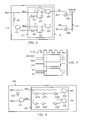
- FIGURE 4 illustrates improved bus arbitrator 110 for use with exemplary shared address or data bus 140 according to an exemplary embodiment of the present invention.
- FIGURE 5 is a timing diagram illustrating the operation of exemplary bus arbitrator 110 in FIGURE 4 according to one embodiment of the present invention.
- Bus arbitrator 110 comprises inverter 405, AND gate 410, and fast turn-off, slow turn-on controller 420.
- Controller 420 comprises inverters 421 and 31, D-gate flip-flops (FF) 422 and 432, and AND gates 423 and 433. Controller 420 is clocked by the CLOCK signal, which causes D-gate flip-flops 422 and 423 to change state on the falling edges of the CLOCK signal.
- controller 420 introduces a one-half clock cycle delay into the bus due to its sequential behavior. This is acceptable in situations in which the hardware resources are synchronous to the system clock and have sufficient timing slack to accommodate this delay. However, in cases where such delay is not acceptable, a combinational delay may be used as illustrated in FIGURE 6, to achieve fast turn-off and slow turn-on times.
- FIGURE 6 illustrates selected portions of improved bus arbitrator 610 according to an alternate embodiment of the present invention.
- Arbitrator 610 is similar to arbitrator 110 in FIGURE 4 except that the synchronous delay elements (i.e., D-gate flip-flops) in fast turn-off, slow turn-on controller 420 have been replaced in fast turn-off, slow turn-on controller 620 by an even number (2N) inverters 622 that introduce the delay.
- synchronous delay elements i.e., D-gate flip-flops
Landscapes
- Engineering & Computer Science (AREA)
- Theoretical Computer Science (AREA)
- General Engineering & Computer Science (AREA)
- Physics & Mathematics (AREA)
- General Physics & Mathematics (AREA)
- Computer Hardware Design (AREA)
- Bus Control (AREA)
Abstract
Description
Claims (13)
- For use in a shared bus system comprising a plurality of bus devices capable of requesting access to a shared bus, a bus arbitrator operable to slowly activate and rapidly de-activate tristate line drivers coupled to said shared bus, said bus arbitrator comprising:an input interface capable of receiving a first bus access request signal from a first of said plurality of bus devices;a delay circuit capable of receiving said first bus access request signal from said input interface and generating therefrom a time-delayed first bus access request signal; anda comparator circuit capable of receiving said first bus access request signal from said input interface and said time-delayed first bus access request signal from said delay circuit and generating a line driver enable signal only if both of said first bus access request signal and said time-delayed first bus access request signal are enabled.
- A shared bus system comprising:N bus devices capable of requesting access to a shared bus;M tristate line drivers, each of said M tristate line drivers having an input for receiving a logic bit from one of said N bus devices and an output for outputting said received logic bit to said shared bus, wherein said each tristate line driver outputs said received logic bit when a line driver enable signal associated with said each tristate line driver is enabled and an output of said each tristate line driver is put into a high-impedance state when said line driver enable signal is disabled; anda bus arbitrator operable to slowly activate and rapidly de-activate said M tristate line drivers, said bus arbitrator comprising:an input interface capable of receiving a first bus access request signal from a first of said N bus devices;a delay circuit capable of receiving said first bus access request signal from said input interface and generating therefrom a time-delayed first bus access request signal; anda comparator circuit capable of receiving said first bus access request signal from said input interface and said time-delayed first bus access request signal from said delay circuit and generating a line driver enable signal only if both of said first bus access request signal and said time-delayed first bus access request signal are enabled.
- The arbitrator or shared bus system as set forth in any preceding Claim wherein comparator circuit disables said line driver enable signal if either of said first bus access request signal and said time-delayed first bus access request signal is disabled.
- The arbitrator or shared bus system as set forth in any preceding Claim wherein a time delay of said delay circuit is greater than a maximum de-activation delay period associated with said tri-state line drivers.
- The arbitrator or shared bus system as set forth in any preceding Claim wherein said comparator circuit comprises an AND gate having a first input for receiving said first bus access request and a second input for receiving said time-delayed first bus access request signal.
- The arbitrator or shared bus system as set forth in any preceding Claim wherein said delay circuit is an asynchronous delay circuit.
- The arbitrator or shared bus system as set forth in any preceding Claim wherein said delay circuit comprises an even number of inverters connected in series, wherein a first of said even number of inverters receives said first bus access request signal from said input interface and a last of said even number of inverters generates said time-delayed first bus access request signal.
- The arbitrator or shared bus system as set forth in any preceding Claim wherein said delay circuit is a synchronous delay circuit.
- The arbitrator or shared bus system as set forth in any preceding Claims wherein said delay circuit comprises a flip-flop having an input capable of receiving said first bus access request signal from said input interface and an output coupled to said comparator circuit that generates said time-delayed first bus access request signal.
- For use in a shared bus system comprising N bus devices capable of requesting access to a shared bus, a method for slowly activating and rapidly de-activating a plurality of tristate line drivers coupled between the shared bus and the N bus devices, the method comprising the steps of:receiving a first bus access request signal from a first of the plurality of bus devices;generating from the first bus access request signal a time-delayed first bus access request signal; andcomparing in a comparator circuit the first bus access request signal and the time-delayed first bus access request signal and generating a line driver enable signal only if both of the first bus access request signal and the time-delayed first bus access request signal are enabled.
- The method as set forth in Claim 10 further comprising the step of disabling the line driver enable signal if either of the first bus access request signal and the time-delayed first bus access request signal is disabled.
- The method as set forth in Claim 10 or 11 wherein a time delay associated with the time-delayed first bus access request signal is greater than a maximum de-activation delay period associated with the plurality of tri-state line drivers.
- The method as set forth in Claim 10, 11 or 12 wherein the comparator circuit comprises an AND gate having a first input for receiving the first bus access request and a second input for receiving the time-delayed first bus access request signal.
Applications Claiming Priority (2)
| Application Number | Priority Date | Filing Date | Title |
|---|---|---|---|
| US60454 | 1993-05-10 | ||
| US10/060,454 US7203779B2 (en) | 2002-01-30 | 2002-01-30 | Fast turn-off slow turn-on arbitrator for reducing tri-state driver power dissipation on a shared bus |
Publications (2)
| Publication Number | Publication Date |
|---|---|
| EP1335294A2 true EP1335294A2 (en) | 2003-08-13 |
| EP1335294A3 EP1335294A3 (en) | 2007-05-09 |
Family
ID=27609987
Family Applications (1)
| Application Number | Title | Priority Date | Filing Date |
|---|---|---|---|
| EP03250548A Withdrawn EP1335294A3 (en) | 2002-01-30 | 2003-01-29 | Fast turn-off slow turn-on arbitrator for reducing tri-state driver power dissipation on a shared bus |
Country Status (2)
| Country | Link |
|---|---|
| US (1) | US7203779B2 (en) |
| EP (1) | EP1335294A3 (en) |
Cited By (1)
| Publication number | Priority date | Publication date | Assignee | Title |
|---|---|---|---|---|
| CN1304973C (en) * | 2003-11-14 | 2007-03-14 | 威盛电子股份有限公司 | Apparatus and method for obtaining a bus control |
Families Citing this family (6)
| Publication number | Priority date | Publication date | Assignee | Title |
|---|---|---|---|---|
| US8127309B1 (en) * | 2006-11-10 | 2012-02-28 | Marvell International Ltd. | Secure digital input/output interface system |
| US7962670B2 (en) * | 2007-06-06 | 2011-06-14 | Lantiq Deutschland Gmbh | Pin multiplexing |
| EP2302519B1 (en) * | 2009-09-09 | 2013-01-16 | ST-Ericsson SA | Dynamic frequency memory control |
| US10079049B2 (en) | 2016-06-08 | 2018-09-18 | Micron Technology, Inc. | Stack access control for memory device |
| US10282264B1 (en) | 2017-11-09 | 2019-05-07 | Micron Technology, Inc. | Apparatus and methods for repairing memory devices including a plurality of memory die and an interface |
| US12255644B2 (en) * | 2022-11-28 | 2025-03-18 | Texas Instruments Incorporated | Audio interface physical layer |
Family Cites Families (10)
| Publication number | Priority date | Publication date | Assignee | Title |
|---|---|---|---|---|
| US3886543A (en) * | 1973-11-29 | 1975-05-27 | Teletype Corp | Debounce logic for keyboard |
| JPS61195449A (en) * | 1985-02-26 | 1986-08-29 | Toshiba Corp | Bus control method |
| US5029076A (en) * | 1986-01-29 | 1991-07-02 | Digital Equipment Corporation | Apparatus and method for providing a settling time cycle for a system bus in a data processing system |
| ES2002950A6 (en) * | 1986-01-29 | 1988-10-01 | Digital Equipment Corp | Apparatus and method for providing a settling time cycle for a system bus in a data processing system. |
| JPH06101227B2 (en) * | 1986-11-29 | 1994-12-12 | 三菱電機株式会社 | Semiconductor memory device |
| US5044167A (en) * | 1990-07-10 | 1991-09-03 | Sundstrand Corporation | Vapor cycle cooling system having a compressor rotor supported with hydrodynamic compressor bearings |
| US5319768A (en) * | 1991-05-01 | 1994-06-07 | Sgs-Thomson Microelectronics, Inc. | Control circuit for resetting a snoop valid bit in a dual port cache tag memory |
| US5306963A (en) * | 1992-06-19 | 1994-04-26 | Intel Corporation | Address transition detection noise filter in pulse summation circuit for nonvolatile semiconductor memory |
| CA2254310C (en) * | 1997-11-17 | 2001-06-05 | Mitel Corporation | Method of selecting between multiple clock drive sources for a backplane clock signal |
| US6566907B1 (en) * | 2001-11-08 | 2003-05-20 | Xilinx, Inc. | Unclocked digital sequencer circuit with flexibly ordered output signal edges |
-
2002
- 2002-01-30 US US10/060,454 patent/US7203779B2/en not_active Expired - Lifetime
-
2003
- 2003-01-29 EP EP03250548A patent/EP1335294A3/en not_active Withdrawn
Cited By (1)
| Publication number | Priority date | Publication date | Assignee | Title |
|---|---|---|---|---|
| CN1304973C (en) * | 2003-11-14 | 2007-03-14 | 威盛电子股份有限公司 | Apparatus and method for obtaining a bus control |
Also Published As
| Publication number | Publication date |
|---|---|
| EP1335294A3 (en) | 2007-05-09 |
| US7203779B2 (en) | 2007-04-10 |
| US20030145145A1 (en) | 2003-07-31 |
Similar Documents
| Publication | Publication Date | Title |
|---|---|---|
| US7266632B2 (en) | Programmable logic device including programmable interface core and central processing unit | |
| US5420808A (en) | Circuitry and method for reducing power consumption within an electronic circuit | |
| CN113066516B (en) | Method for multiplexing power signals between voltage-limited circuits | |
| US6163848A (en) | System and method for re-starting a peripheral bus clock signal and requesting mastership of a peripheral bus | |
| KR20170116042A (en) | Independent Power Cole Labs Methodology | |
| US6714051B2 (en) | Logic circuitry-implemented bus buffer | |
| JP2004506975A (en) | Efficient clock start and stop mechanism for clock-forwarded system I/O - Patents.com | |
| US7203779B2 (en) | Fast turn-off slow turn-on arbitrator for reducing tri-state driver power dissipation on a shared bus | |
| JP2003518631A (en) | Low power scan flip-flop | |
| KR20250029732A (en) | Arbiter for non-persistent signals | |
| JP2579237B2 (en) | State element circuit having a flow-through latch circuit, VLSI circuit having the state element circuit, and method of operating a latch as a functional alternative to a master-slave flip-flop | |
| Nedovic et al. | Dynamic flip-flop with improved power | |
| US5767701A (en) | Synchronous contention prevention logic for bi-directional signals | |
| Dasgupta et al. | 8.4 radeon RX 5700 series: The AMD 7nm energy-efficient high-performance GPUs | |
| US20070011366A1 (en) | Bus system and data transfer method | |
| US6269102B1 (en) | Bus control device | |
| US6121814A (en) | Tri-state bus controller | |
| US7436220B2 (en) | Partially gated mux-latch keeper | |
| US6484267B1 (en) | Clock gated bus keeper | |
| US5802317A (en) | Electronic circuit having phased logic busses for reducing electromagnetic interference | |
| US5872937A (en) | System for optimizing bus arbitration latency and method therefor | |
| CN114978124A (en) | Clock oscillator control circuit | |
| US12580568B2 (en) | Scalable arbiter for non-persistent signals | |
| US7698514B2 (en) | Data processing system and method for interconnect arbitration | |
| JP3721074B2 (en) | Method for transferring data between a sending device and a receiving device via a bus |
Legal Events
| Date | Code | Title | Description |
|---|---|---|---|
| PUAI | Public reference made under article 153(3) epc to a published international application that has entered the european phase |
Free format text: ORIGINAL CODE: 0009012 |
|
| AK | Designated contracting states |
Designated state(s): AT BE BG CH CY CZ DE DK EE ES FI FR GB GR HU IE IT LI LU MC NL PT SE SI SK TR |
|
| AX | Request for extension of the european patent |
Extension state: AL LT LV MK RO |
|
| PUAL | Search report despatched |
Free format text: ORIGINAL CODE: 0009013 |
|
| AK | Designated contracting states |
Kind code of ref document: A3 Designated state(s): AT BE BG CH CY CZ DE DK EE ES FI FR GB GR HU IE IT LI LU MC NL PT SE SI SK TR |
|
| AX | Request for extension of the european patent |
Extension state: AL LT LV MK RO |
|
| 17P | Request for examination filed |
Effective date: 20071030 |
|
| STAA | Information on the status of an ep patent application or granted ep patent |
Free format text: STATUS: THE APPLICATION HAS BEEN WITHDRAWN |
|
| 17Q | First examination report despatched |
Effective date: 20071214 |
|
| 18W | Application withdrawn |
Effective date: 20071205 |
|
| AKX | Designation fees paid |
Designated state(s): DE FR GB IT |