EP1335239B1 - Conversion between optical and radio frequency signals - Google Patents
Conversion between optical and radio frequency signals Download PDFInfo
- Publication number
- EP1335239B1 EP1335239B1 EP02290319A EP02290319A EP1335239B1 EP 1335239 B1 EP1335239 B1 EP 1335239B1 EP 02290319 A EP02290319 A EP 02290319A EP 02290319 A EP02290319 A EP 02290319A EP 1335239 B1 EP1335239 B1 EP 1335239B1
- Authority
- EP
- European Patent Office
- Prior art keywords
- radio signal
- optical
- guide
- radio
- interaction
- Prior art date
- Legal status (The legal status is an assumption and is not a legal conclusion. Google has not performed a legal analysis and makes no representation as to the accuracy of the status listed.)
- Expired - Lifetime
Links
- 230000003287 optical effect Effects 0.000 title claims abstract description 94
- 238000006243 chemical reaction Methods 0.000 title 1
- 230000003993 interaction Effects 0.000 claims abstract description 31
- 239000000463 material Substances 0.000 claims abstract description 28
- 230000008878 coupling Effects 0.000 claims abstract description 13
- 238000010168 coupling process Methods 0.000 claims abstract description 13
- 238000005859 coupling reaction Methods 0.000 claims abstract description 13
- 230000001902 propagating effect Effects 0.000 claims abstract description 5
- DMLAVOWQYNRWNQ-UHFFFAOYSA-N azobenzene Chemical compound C1=CC=CC=C1N=NC1=CC=CC=C1 DMLAVOWQYNRWNQ-UHFFFAOYSA-N 0.000 claims description 4
- 239000011159 matrix material Substances 0.000 claims description 4
- 230000000644 propagated effect Effects 0.000 claims description 4
- 239000002861 polymer material Substances 0.000 claims description 3
- 230000007704 transition Effects 0.000 abstract description 5
- 239000013307 optical fiber Substances 0.000 description 7
- 230000005855 radiation Effects 0.000 description 7
- 238000010521 absorption reaction Methods 0.000 description 5
- 229920000642 polymer Polymers 0.000 description 4
- 238000004891 communication Methods 0.000 description 3
- 238000001514 detection method Methods 0.000 description 3
- 230000005684 electric field Effects 0.000 description 3
- 238000000034 method Methods 0.000 description 3
- VYPSYNLAJGMNEJ-UHFFFAOYSA-N Silicium dioxide Chemical compound O=[Si]=O VYPSYNLAJGMNEJ-UHFFFAOYSA-N 0.000 description 2
- 230000005540 biological transmission Effects 0.000 description 2
- 238000010276 construction Methods 0.000 description 2
- 239000006185 dispersion Substances 0.000 description 2
- 238000005516 engineering process Methods 0.000 description 2
- 238000004519 manufacturing process Methods 0.000 description 2
- 229910052751 metal Inorganic materials 0.000 description 2
- 239000002184 metal Substances 0.000 description 2
- 239000004065 semiconductor Substances 0.000 description 2
- 230000003595 spectral effect Effects 0.000 description 2
- 239000000126 substance Substances 0.000 description 2
- FOQABOMYTOFLPZ-ISLYRVAYSA-N Disperse Red 1 Chemical compound C1=CC(N(CCO)CC)=CC=C1\N=N\C1=CC=C([N+]([O-])=O)C=C1 FOQABOMYTOFLPZ-ISLYRVAYSA-N 0.000 description 1
- RTAQQCXQSZGOHL-UHFFFAOYSA-N Titanium Chemical compound [Ti] RTAQQCXQSZGOHL-UHFFFAOYSA-N 0.000 description 1
- 239000004566 building material Substances 0.000 description 1
- 239000000969 carrier Substances 0.000 description 1
- 238000004132 cross linking Methods 0.000 description 1
- 238000000354 decomposition reaction Methods 0.000 description 1
- 238000010586 diagram Methods 0.000 description 1
- 230000005672 electromagnetic field Effects 0.000 description 1
- 238000000605 extraction Methods 0.000 description 1
- 229920002313 fluoropolymer Polymers 0.000 description 1
- PCHJSUWPFVWCPO-UHFFFAOYSA-N gold Chemical compound [Au] PCHJSUWPFVWCPO-UHFFFAOYSA-N 0.000 description 1
- 239000010931 gold Substances 0.000 description 1
- 229910052737 gold Inorganic materials 0.000 description 1
- 230000006698 induction Effects 0.000 description 1
- 238000003780 insertion Methods 0.000 description 1
- 230000037431 insertion Effects 0.000 description 1
- GQYHUHYESMUTHG-UHFFFAOYSA-N lithium niobate Chemical compound [Li+].[O-][Nb](=O)=O GQYHUHYESMUTHG-UHFFFAOYSA-N 0.000 description 1
- 239000013308 plastic optical fiber Substances 0.000 description 1
- 230000010287 polarization Effects 0.000 description 1
- 229920003229 poly(methyl methacrylate) Polymers 0.000 description 1
- 239000004926 polymethyl methacrylate Substances 0.000 description 1
- 230000006798 recombination Effects 0.000 description 1
- 238000005215 recombination Methods 0.000 description 1
- 230000009467 reduction Effects 0.000 description 1
- 239000000377 silicon dioxide Substances 0.000 description 1
- 238000001228 spectrum Methods 0.000 description 1
- 239000010936 titanium Substances 0.000 description 1
- 229910052719 titanium Inorganic materials 0.000 description 1
Images


Classifications
-
- G—PHYSICS
- G02—OPTICS
- G02F—OPTICAL DEVICES OR ARRANGEMENTS FOR THE CONTROL OF LIGHT BY MODIFICATION OF THE OPTICAL PROPERTIES OF THE MEDIA OF THE ELEMENTS INVOLVED THEREIN; NON-LINEAR OPTICS; FREQUENCY-CHANGING OF LIGHT; OPTICAL LOGIC ELEMENTS; OPTICAL ANALOGUE/DIGITAL CONVERTERS
- G02F2/00—Demodulating light; Transferring the modulation of modulated light; Frequency-changing of light
-
- G—PHYSICS
- G02—OPTICS
- G02F—OPTICAL DEVICES OR ARRANGEMENTS FOR THE CONTROL OF LIGHT BY MODIFICATION OF THE OPTICAL PROPERTIES OF THE MEDIA OF THE ELEMENTS INVOLVED THEREIN; NON-LINEAR OPTICS; FREQUENCY-CHANGING OF LIGHT; OPTICAL LOGIC ELEMENTS; OPTICAL ANALOGUE/DIGITAL CONVERTERS
- G02F1/00—Devices or arrangements for the control of the intensity, colour, phase, polarisation or direction of light arriving from an independent light source, e.g. switching, gating or modulating; Non-linear optics
- G02F1/01—Devices or arrangements for the control of the intensity, colour, phase, polarisation or direction of light arriving from an independent light source, e.g. switching, gating or modulating; Non-linear optics for the control of the intensity, phase, polarisation or colour
- G02F1/061—Devices or arrangements for the control of the intensity, colour, phase, polarisation or direction of light arriving from an independent light source, e.g. switching, gating or modulating; Non-linear optics for the control of the intensity, phase, polarisation or colour based on electro-optical organic material
- G02F1/065—Devices or arrangements for the control of the intensity, colour, phase, polarisation or direction of light arriving from an independent light source, e.g. switching, gating or modulating; Non-linear optics for the control of the intensity, phase, polarisation or colour based on electro-optical organic material in an optical waveguide structure
-
- G—PHYSICS
- G02—OPTICS
- G02F—OPTICAL DEVICES OR ARRANGEMENTS FOR THE CONTROL OF LIGHT BY MODIFICATION OF THE OPTICAL PROPERTIES OF THE MEDIA OF THE ELEMENTS INVOLVED THEREIN; NON-LINEAR OPTICS; FREQUENCY-CHANGING OF LIGHT; OPTICAL LOGIC ELEMENTS; OPTICAL ANALOGUE/DIGITAL CONVERTERS
- G02F1/00—Devices or arrangements for the control of the intensity, colour, phase, polarisation or direction of light arriving from an independent light source, e.g. switching, gating or modulating; Non-linear optics
- G02F1/01—Devices or arrangements for the control of the intensity, colour, phase, polarisation or direction of light arriving from an independent light source, e.g. switching, gating or modulating; Non-linear optics for the control of the intensity, phase, polarisation or colour
- G02F1/015—Devices or arrangements for the control of the intensity, colour, phase, polarisation or direction of light arriving from an independent light source, e.g. switching, gating or modulating; Non-linear optics for the control of the intensity, phase, polarisation or colour based on semiconductor elements having potential barriers, e.g. having a PN or PIN junction
- G02F1/025—Devices or arrangements for the control of the intensity, colour, phase, polarisation or direction of light arriving from an independent light source, e.g. switching, gating or modulating; Non-linear optics for the control of the intensity, phase, polarisation or colour based on semiconductor elements having potential barriers, e.g. having a PN or PIN junction in an optical waveguide structure
-
- G—PHYSICS
- G02—OPTICS
- G02F—OPTICAL DEVICES OR ARRANGEMENTS FOR THE CONTROL OF LIGHT BY MODIFICATION OF THE OPTICAL PROPERTIES OF THE MEDIA OF THE ELEMENTS INVOLVED THEREIN; NON-LINEAR OPTICS; FREQUENCY-CHANGING OF LIGHT; OPTICAL LOGIC ELEMENTS; OPTICAL ANALOGUE/DIGITAL CONVERTERS
- G02F1/00—Devices or arrangements for the control of the intensity, colour, phase, polarisation or direction of light arriving from an independent light source, e.g. switching, gating or modulating; Non-linear optics
- G02F1/01—Devices or arrangements for the control of the intensity, colour, phase, polarisation or direction of light arriving from an independent light source, e.g. switching, gating or modulating; Non-linear optics for the control of the intensity, phase, polarisation or colour
- G02F1/03—Devices or arrangements for the control of the intensity, colour, phase, polarisation or direction of light arriving from an independent light source, e.g. switching, gating or modulating; Non-linear optics for the control of the intensity, phase, polarisation or colour based on ceramics or electro-optical crystals, e.g. exhibiting Pockels effect or Kerr effect
- G02F1/035—Devices or arrangements for the control of the intensity, colour, phase, polarisation or direction of light arriving from an independent light source, e.g. switching, gating or modulating; Non-linear optics for the control of the intensity, phase, polarisation or colour based on ceramics or electro-optical crystals, e.g. exhibiting Pockels effect or Kerr effect in an optical waveguide structure
- G02F1/0356—Devices or arrangements for the control of the intensity, colour, phase, polarisation or direction of light arriving from an independent light source, e.g. switching, gating or modulating; Non-linear optics for the control of the intensity, phase, polarisation or colour based on ceramics or electro-optical crystals, e.g. exhibiting Pockels effect or Kerr effect in an optical waveguide structure controlled by a high-frequency electromagnetic wave component in an electric waveguide structure
-
- G—PHYSICS
- G02—OPTICS
- G02F—OPTICAL DEVICES OR ARRANGEMENTS FOR THE CONTROL OF LIGHT BY MODIFICATION OF THE OPTICAL PROPERTIES OF THE MEDIA OF THE ELEMENTS INVOLVED THEREIN; NON-LINEAR OPTICS; FREQUENCY-CHANGING OF LIGHT; OPTICAL LOGIC ELEMENTS; OPTICAL ANALOGUE/DIGITAL CONVERTERS
- G02F1/00—Devices or arrangements for the control of the intensity, colour, phase, polarisation or direction of light arriving from an independent light source, e.g. switching, gating or modulating; Non-linear optics
- G02F1/29—Devices or arrangements for the control of the intensity, colour, phase, polarisation or direction of light arriving from an independent light source, e.g. switching, gating or modulating; Non-linear optics for the control of the position or the direction of light beams, i.e. deflection
- G02F1/33—Acousto-optical deflection devices
- G02F1/335—Acousto-optical deflection devices having an optical waveguide structure
-
- G—PHYSICS
- G02—OPTICS
- G02F—OPTICAL DEVICES OR ARRANGEMENTS FOR THE CONTROL OF LIGHT BY MODIFICATION OF THE OPTICAL PROPERTIES OF THE MEDIA OF THE ELEMENTS INVOLVED THEREIN; NON-LINEAR OPTICS; FREQUENCY-CHANGING OF LIGHT; OPTICAL LOGIC ELEMENTS; OPTICAL ANALOGUE/DIGITAL CONVERTERS
- G02F2/00—Demodulating light; Transferring the modulation of modulated light; Frequency-changing of light
- G02F2/02—Frequency-changing of light, e.g. by quantum counters
-
- H—ELECTRICITY
- H04—ELECTRIC COMMUNICATION TECHNIQUE
- H04B—TRANSMISSION
- H04B10/00—Transmission systems employing electromagnetic waves other than radio-waves, e.g. infrared, visible or ultraviolet light, or employing corpuscular radiation, e.g. quantum communication
- H04B10/25—Arrangements specific to fibre transmission
- H04B10/2575—Radio-over-fibre, e.g. radio frequency signal modulated onto an optical carrier
- H04B10/25752—Optical arrangements for wireless networks
Definitions
- This invention relates to radio frequency modulated optical radiation and, more particularly, to apparatus for generating modulated optical signals and to apparatus for detecting radio signals modulated on optical signals.
- Radio frequency modulated optical fibres systems such as those described in US Patent specification N° 5917636 enable a mobile network to be built covering wide areas. These systems are capable of accepting continuous increase in demand in terms of data rate and free spectrum range and of expansion of the equipment and infrastructure installed.
- the increase of frequency of these systems enables a reduction in the size of the antennae and devices used in the radio frequency part of the network and an increase in the bandwidth of the whole system.
- two spectral ranges of 62-63GHz and 65-66GHz which are still unallocated by ITU, have been identified within the framework of the NBS project (RACE 2067) as particularly suitable for such systems.
- the present invention is applicable to these frequency ranges and other frequencies, especially but not exclusively in the so-called millimetric radio frequency ranges, where the wavelength of the radio signal in free air is of the order of one to ten millimetres.
- Such radio signals may be subject to strong absorption by the atmosphere and by common building materials, so that it is of particular interest transmission for the radio signals to be modulated onto an optical signal that is guided in an optical fibre from a source to a so-called pico-cell, where the radio signal may be detected and, if desired, radiated over a relatively short distance.
- generation of the modulated optical signals is preferably obtained by combining two phase-correlated optical carriers which are generated in a dual-frequency laser transmitter with a frequency offset equal to the desired microwave frequency of the radio carrier signal.
- the two optical signals are then transmitted through optical fibre and the radio signal is recovered in a detector.
- FIG. 1 An example of a communication system of this kind, which may be used in a system in accordance with the present invention, is shown in Figure 1 and comprises, at the transmitter end, a master laser 1, connected by optical fibre 2 to a radio frequency modulator 3, which in turn is connected by optical fibre 4 to a beam splitter 5.
- the two optical signals from the beam splitter 5 are connected by optical fibres 6 to two slave lasers 7 tuned to frequencies spaced apart by an amount equal to the radio signal frequency, which act as filters to generate optical signals with a high degree of phase correlation and spectral purity.
- the outputs of the slave lasers 7 are connected to a recombination device 8 before transmission over the optical fibre output line 9.
- the system comprises a detector 10 that receives the optical signals in the optical fibre line 9 and demodulates the radio signals.
- the radio signal detector described in that article is a photodetector.
- the present invention provides apparatus for converting between optical and radio frequency signals as described in the accompanying claims.
- FIG. 2 to 6 of the drawings show apparatus for converting between optical and radio frequency signals in accordance with one embodiment of the present invention.
- the apparatus shown in Figures 2 to 6 of the drawings is an optical to radio frequency detector and this embodiment of the invention is described with reference to a detector; however, it will be appreciated that similar design principles can be applied to a modulator for modulating an optical signal with a radio frequency signal.
- the design principles are also applicable to a transceiver, that is to say a device that receives optical signals modulated by a first radio signals and detects the first radio signals, and modulates the optical signals with a second radio signal that is transmitted elsewhere.
- Figure 1 of the drawings shows a communication system as described above including a modulator 3 and a detector 10.
- the detector 10 of the system is of the kind illustrated in Figures 2 to 6 of the accompanying drawings.
- the modulator is also of the kind shown in Figures 2 to 6 of the drawings, but with a single optical input signal and a radio frequency input signal instead of the two optical input signals and radio frequency output signal of the detector.
- the detector is a passive detector comprising an optical ridge wave-guide.
- a construction of an optical ridge wave-guide is described in the article "The single-mode condition for semiconductor wave-guides with large cross-section" in the Journal of Light Wave Technology, Volume 16, pages 1851 to 1853, for example.
- the optical guide used is based on the principle of total reflection at the interface between two mediums of different refractive index.
- the optical ridge wave-guide comprises upper and lower buffer layers 11 and 12.
- An electro-optic core is positioned in intimate contact between the upper and lower buffer layers 11 and 12, the electro-optic core 10 comprising a layer 13 of thickness substantially less than the wavelength of the optical radiation and a ridge 14 of thickness comparable to the wavelength of the optical radiation and of width greater than the wavelength of the optical radiation.
- the wavelength of the optical radiation is 1.55 microns
- the thickness of the layer 13 is 0.2 microns
- the thickness of the ridge 14 is 1.5 microns
- the width of the ridge being 4 microns.
- the interaction material of the electro-optic guide 13, 14 presents a second-order non-linear optical polarisation characteristic to the propagation of the optical signal components and more particularly is a dipolar material presenting non-centre-symmetric interaction characteristics in a host matrix polymer material.
- a suitable interaction material of this kind comprises electrically orientated diazobenzene.
- the electrically orientated diazobenzene is an active chromophore "Disperse Red 1" grafted to polymethylmetacrylate as host matrix ("PMMA-DR1").
- PMMA-DR1 active chromophore
- the chemical formula of PMMA-DR1 is shown in Figure 4, the left hand side of the formula being the active dipolar DR1 and the right hand side being the host PMMA.
- a molecule of this type placed in an electric field orients in such a way as to align with the field.
- an orientated material can be obtained in which the polar molecules are statistically directed in similar directions to give second order non-linear optical polarisation properties, and in particular non-centre-symmetric properties.
- the electro-optic core 13, 14 is formed in PMMA-DR1.
- the component is heated to the vitreous transition point of the electro-optic core polymer, approximately 120°C.
- An intense electric field is applied to the metal layers used as electrodes. The electric field is maintained subsequently while the temperature is reduced towards ambient temperature.
- the buffer layers 11 and 12 are produced in fluorinated polymers "AVO14" and “AVO01” described in the article "Fabrication of low refractive index low loss fluorinated self-cross linking polymer waveguides for optical devices" in the Proceedings of the 7 th International Plastic Optical Fibres Conference 1998, pages 316 to 323. These materials are chosen for their refractive index, which is less than that of the electro-optic core. At the wavelength of the optical radiation in the present example, 1.55 microns, the refractive index of PMMA-DR1 is 1.5965, the refractive index of AVO01 is 1.4466 and that of AVO14 is 1.4009.
- the electro-optic core ridge 14 is connected with input and output optical fibres (not shown) by respective linear tapers (not shown), which adapt the shape and size of the optical fibre (typically diameter 10 microns) to the shape (rectangular cross-section) and size (approximately 4 microns) of the electro-optic core ridge 14 while reducing insertion and extraction losses.
- the device shown in the drawings also includes a radio signal guide in travelling wave coupling with the optical guide formed by the electro-optic core 10.
- Various radio signal wave-guides may be used, such as a strip-line in which a strip extends between two ground planes, or a coplanar wave-guide in which a strip extends in the same plane as two lateral grounded strips, or a grounded coplanar wave-guide in which a coplanar wave-guide extends parallel to a grounded plane.
- the radio signal guide is a microstrip guide comprising a strip of width approximately 15 microns, compared with a width of approximately 4 microns for the optical wave-guide electro-optic core ridge 14, juxtaposed with a ground plane metallic layer 16 on the opposite side of the electro-optic core ridge 14.
- the spacing and width of the strip 15 and ground plane layer 16 are chosen so that the impedance of the microstrip at the radio signal frequency (60GHz in this example) are compatible with standard wave-guides such as the WR15 wave-guide (50ohms).
- the standard dimensions of a WR15 wave-guide are as follows: Band Frequ. range Internal dims (mm) External dims (mm) Cut-off frequ. Losses (dB/m) width height width height V 50-75 GHz 0.3759 0.1879 0.579 0.391 39.9 GHz 0.188
- the strip 15 is closely juxtaposed with the top surface of the upper buffer 11 and the ground plane 16 is closely juxtaposed with the bottom surface of the lower buffer 12.
- the length over which the microstrip 15 is in close coupling with the optical guide is chosen to be at least approximately equal to the wavelength of the radio signal, that is to say, at least 5 millimetres at the radio signal frequency of 60GHz in this example; in the preferred embodiment of the invention, the optical/radio interaction length for this frequency is 1.3cm. In this way, a travelling wave coupling is obtained that is found to be particularly effective for the efficiency of the device.
- the dimensions of the elements of the device and the characteristics of the materials used are chosen so that the propagation velocities of the optical signal components in the optical guide and of the radio signal in the radio signal guide are substantially equal. Again, this characteristic is found to be important for the efficiency of detection (or modulation in the case of a modulator).
- E and H are respectively the electrical and induction fields.
- P NL represents the non-linear polarization and is defined by:
- ⁇ i,j,k represent the different frequencies and ⁇ the non linear suceptibility of the propagation medium.
- guided mode formalism is used, where the different fields are split on an orthogonal basis constituted by the local modes, as shown by the following equation:
- E rad and H rad are the radiating parts of the electromagnetic field. Then, using the orthogonal properties of this decomposition, the variation of the amplitude of each wavelength is deduced from (1) and (3):
- the ⁇ coefficients represent the overlap of the three fields. Finally account is taken of the absorption of the propagation medium by introducing a complex value for ⁇ k in the treatment of the system (4).
- the ground plane 16 is formed from a layer of gold deposited on a layer of titanium that is itself deposited on a layer of silica 17 serving as a support.
- the microstrip radio signal guide 15 extending parallel to and juxtaposed with the optical guide 14 is connected with external radio signal wave-guides (one of which is shown at 18 in Figures 5 and 6 of WR15 type (standard wave-guides for 50 to 75 GHz radio frequencies).
- the WR15 wave-guides extend perpendicularly to the length of the microstrip radio signal guide 15 and the optical guide 14 and parallel to the ground plane 16.
- Transition radio signal guide elements 20 and 21 are formed in the material of the ground plane 16 and present progressively varying cross sections to match the propagation characteristics of the microstrip with the WR15 wave-guides. More specifically, the guide elements 20 and 21 comprise "Vivaldi antenna" openings in the ground planes 16 of trumpet shape, of which the small end is of similar width to the microstrip 15 and the large end is of similar width to the corresponding width ('height') of the wave-guide WR15, such as 18.
- the Vivaldi antenna 21 is connected with the receiver circuit elements (for example, to a re-transmission circuit) while the Vivaldi antenna 20 is connected to a n element presenting a matching load to the microstrip 15, to ensure that it functions in balanced conditions.
- the microstrip element 15 traverses the small end of the Vivaldi antennas 20 and 21, spaced from them by the thickness of the stacked buffer layers 11 and 12 and the electro-optic layer 13, 14.
- the microstrip 15 includes extensions 22 and 23 that are parallel with, but staggered relative to, the part of the microstrip 15 in radio signal coupling relationship with the optical guide 14.
- the small ends of the Vivaldi antennas 20 and 21 are also spaced relative to the optical guide 14.
- the small ends of the Vivaldi antennas 20 and 21 are disposed directly beneath the optical guide 14 and the microstrip-line 15 is entirely in line with the optical guide 14 and in radio signal coupling relationship therewith.
- radio signal frequency resonators 24, 25 are formed in the shape of quadrant (or "fan") resonators as extensions of the ends of the microstrip 15 and resonators 26, 27 are formed as extensions of the openings at the small ends of the Vivaldi antennas 20 and 21.
- the resonators are designed with dimensions such that they present termination impedances matched to the impedances of the microstrip 15 and the Vivaldi antenna 20,21, respectively, at the operating radio frequency. They effectively minimise the termination reflection coefficient in the plane of propagation of the radio signal in the corresponding element.
- the Vivaldi antennas 20 and 21 are preferably 7.8 microns wide at the small end and 1.879mm wide at the wide end and 3mm long.
- the resonators 26 and 27 of the Vivaldi antennas are preferably of radius 0.56mm and the resonators 24 and 25 of the microstrip are preferably of radius 0.62mm.
- two optical signal components having frequencies that differ by an amount corresponding to the radio signal carrier frequency are applied to the optical input of the optical guide 14.
- the two optical components interact in the second-order non-linear optical polarisation material of the electro-optical core 14.
- the close coupling of the microstrip 15 and ground plane 16 with the optical guide 14 causes the radio frequency signals that result to be induced in the microstrip-line 15.
- the line 15, together with its extensions 22 and 23 in the case of the embodiment shown in Figure 2, and the Vivaldi antennas 20 and 21 extending within the WR15 wave-guides as shown in Figure 4 transmit the radio frequency signal to the WR15 wave-guide 18 and the radio signal is received in the wave-guide.
- a radio signal propagated in the WR15 wave-guide with a single optical component propagated in the optical guide modulates the optical component so that at the output of the optical wave-guide two optical components are propagated.
- the output power of the electrical signal in the case of the detector device shown in the drawings is proportional to the square of the radio frequency, so that substantially higher efficiencies are obtained than in other devices whose efficiency reduces with frequency.
- the output of the radio signal is also proportional to the square of the interaction link and to the square of the input power of the optical signal: consequently the device is more efficient the more intense the optical signals but, concerning the interaction links, absorption of the optical signals in the optical guide limits the length of the optimum interaction link.
Landscapes
- Physics & Mathematics (AREA)
- Nonlinear Science (AREA)
- Optics & Photonics (AREA)
- General Physics & Mathematics (AREA)
- Engineering & Computer Science (AREA)
- Electromagnetism (AREA)
- Crystallography & Structural Chemistry (AREA)
- Ceramic Engineering (AREA)
- Chemical & Material Sciences (AREA)
- Computer Networks & Wireless Communication (AREA)
- Signal Processing (AREA)
- Optical Communication System (AREA)
- Optical Modulation, Optical Deflection, Nonlinear Optics, Optical Demodulation, Optical Logic Elements (AREA)
- Optical Head (AREA)
- Transmitters (AREA)
Abstract
Description
- This invention relates to radio frequency modulated optical radiation and, more particularly, to apparatus for generating modulated optical signals and to apparatus for detecting radio signals modulated on optical signals.
- Radio frequency modulated optical fibres systems, such as those described in US Patent specification N° 5917636 enable a mobile network to be built covering wide areas. These systems are capable of accepting continuous increase in demand in terms of data rate and free spectrum range and of expansion of the equipment and infrastructure installed. The increase of frequency of these systems enables a reduction in the size of the antennae and devices used in the radio frequency part of the network and an increase in the bandwidth of the whole system. For data rates of 155MBit/s and higher, two spectral ranges of 62-63GHz and 65-66GHz, which are still unallocated by ITU, have been identified within the framework of the NBS project (RACE 2067) as particularly suitable for such systems.
- The present invention is applicable to these frequency ranges and other frequencies, especially but not exclusively in the so-called millimetric radio frequency ranges, where the wavelength of the radio signal in free air is of the order of one to ten millimetres. Such radio signals may be subject to strong absorption by the atmosphere and by common building materials, so that it is of particular interest transmission for the radio signals to be modulated onto an optical signal that is guided in an optical fibre from a source to a so-called pico-cell, where the radio signal may be detected and, if desired, radiated over a relatively short distance.
- In order to minimise problems resulting from chromatic dispersion in the optical fibres, generation of the modulated optical signals is preferably obtained by combining two phase-correlated optical carriers which are generated in a dual-frequency laser transmitter with a frequency offset equal to the desired microwave frequency of the radio carrier signal. The two optical signals are then transmitted through optical fibre and the radio signal is recovered in a detector. Systems of this kind are described for example in the article "Chromatic dispersion in fiber-optic microwave and millimetre wave links" in IEEE Transactions on Microwave Theory and Techniques, volume 44
number 10 pages 1716 to 1724, the article "Multifunctional fiber-optic microwave links based on remote heterodyne detection" in IEEE Transactions on Microwave Theory and Techniques, volume 46 pages 458 to 468, and the article "High bandwidth polymer modulators" in IEEE Transactions on LEOS 96, 18-19 Nov. 96, New York, pages 79-80. - An example of a communication system of this kind, which may be used in a system in accordance with the present invention, is shown in Figure 1 and comprises, at the transmitter end, a
master laser 1, connected byoptical fibre 2 to aradio frequency modulator 3, which in turn is connected byoptical fibre 4 to a beam splitter 5. The two optical signals from the beam splitter 5 are connected by optical fibres 6 to twoslave lasers 7 tuned to frequencies spaced apart by an amount equal to the radio signal frequency, which act as filters to generate optical signals with a high degree of phase correlation and spectral purity. The outputs of theslave lasers 7 are connected to a recombination device 8 before transmission over the optical fibre output line 9. At the receiver end, the system comprises adetector 10 that receives the optical signals in the optical fibre line 9 and demodulates the radio signals. - It is important for the
modulator 3 anddetector 10 to provide efficient generation and detection of the radio frequency modulated optical signals. Many proposals have been made based on the use of semiconductor materials in which the optical and radio waves interact. Thus, US patent specification 5 917 636 discloses the use of an electro-absorption layer comprising a multi-quantum well structure of InGaAsP, whose physical dimensions are very much smaller than the wavelength of the radio signals used. - The article "Ultrawide-band/high frequency photodetectors" in IEEE Transactions on Microwave Theory and Technique, Volume 47 pages 1265 to 1281 discloses the use of photodetector material for the interaction in conjunction with various wave-guide and travelling-wave structures for the radio frequency signal. Once again, the dimensions of the detector material are very much smaller than the radio frequency wavelength.
- The article "High frequency polymer modulators with integrated finline transitions and low Vπ" in IEEE Photonics Technology Letters,
Volume 11 pages 54 to 56 discloses the use of a non-linear optical polymer material in a radio frequency modulator for the optical signal, the material being disposed between two electrodes terminating a radio frequency microstrip wave-guide. The radio signal detector described in that article is a photodetector. - In the known systems, problems arise with the efficiency of the systems and the requirement to provide a stabilised voltage for photodiode and phototransistor devices, whose efficiency reduces further at higher frequencies, especially above 100GHz, for example.
- We have found that critical factors in the design of suitable radio frequency modulator and detector devices for use in such systems, especially passive devices, relate to the choice of electro absorption materials and also to the coupling between the various parts of the devices.
- The present invention provides apparatus for converting between optical and radio frequency signals as described in the accompanying claims.
-
- Figure 1 is a block schematic diagram of a communication system in accordance with one embodiment of the invention,
- Figure 2 is a simplified perspective view of components in a detector in accordance with a preferred embodiment of the invention,
- Figure 3 is a cross-section of the detector of Figure 2,
- Figure 4 is the chemical formula of a dipolar diazobenzene material in a host matrix used in the detector of Figure 2,
- Figure 5 is a perspective view of the detector of Figure 2,
- Figure 6 is a plan view of components in the detector of Figure 2, and
- Figure 7 is a simplified perspective view, similar to Figure 2 of components in a detector in accordance with another preferred embodiment of the invention.
-
- The accompanying drawings show apparatus for converting between optical and radio frequency signals in accordance with one embodiment of the present invention. The apparatus shown in Figures 2 to 6 of the drawings is an optical to radio frequency detector and this embodiment of the invention is described with reference to a detector; however, it will be appreciated that similar design principles can be applied to a modulator for modulating an optical signal with a radio frequency signal. The design principles are also applicable to a transceiver, that is to say a device that receives optical signals modulated by a first radio signals and detects the first radio signals, and modulates the optical signals with a second radio signal that is transmitted elsewhere.
- More specifically, Figure 1 of the drawings shows a communication system as described above including a
modulator 3 and adetector 10. In accordance with this embodiment of the present invention thedetector 10 of the system is of the kind illustrated in Figures 2 to 6 of the accompanying drawings. In the preferred embodiment of the invention, the modulator is also of the kind shown in Figures 2 to 6 of the drawings, but with a single optical input signal and a radio frequency input signal instead of the two optical input signals and radio frequency output signal of the detector. - As shown in Figure 2, the detector is a passive detector comprising an optical ridge wave-guide. A construction of an optical ridge wave-guide is described in the article "The single-mode condition for semiconductor wave-guides with large cross-section" in the Journal of Light Wave Technology,
Volume 16, pages 1851 to 1853, for example. - The optical guide used is based on the principle of total reflection at the interface between two mediums of different refractive index. As shown in Figure 3, the optical ridge wave-guide comprises upper and
lower buffer layers lower buffer layers optic core 10 comprising alayer 13 of thickness substantially less than the wavelength of the optical radiation and aridge 14 of thickness comparable to the wavelength of the optical radiation and of width greater than the wavelength of the optical radiation. In the present example, the wavelength of the optical radiation is 1.55 microns, the thickness of thelayer 13 is 0.2 microns and the thickness of theridge 14 is 1.5 microns, the width of the ridge being 4 microns. - In this embodiment of the invention, the interaction material of the electro-
optic guide Red 1" grafted to polymethylmetacrylate as host matrix ("PMMA-DR1"). The chemical formula of PMMA-DR1 is shown in Figure 4, the left hand side of the formula being the active dipolar DR1 and the right hand side being the host PMMA. A molecule of this type placed in an electric field orients in such a way as to align with the field. Starting from an amorphous material, an orientated material can be obtained in which the polar molecules are statistically directed in similar directions to give second order non-linear optical polarisation properties, and in particular non-centre-symmetric properties. - Other non-centre-symmetric materials that are transparent to infrared radiation exist. In addition to other orientated dipolar materials, lithium niobate and most of the III-V and II-VI materials in multiple layers may be produced with suitable second-order non-linear optical polarisation characteristics. However, in the preferred embodiment, the electro-
optic core - In the preferred method of manufacturing the device, after addition of metal layers (described below) the component is heated to the vitreous transition point of the electro-optic core polymer, approximately 120°C. An intense electric field is applied to the metal layers used as electrodes. The electric field is maintained subsequently while the temperature is reduced towards ambient temperature.
- In the preferred embodiment of the invention, the
buffer layers - The electro-
optic core ridge 14 is connected with input and output optical fibres (not shown) by respective linear tapers (not shown), which adapt the shape and size of the optical fibre (typicallydiameter 10 microns) to the shape (rectangular cross-section) and size (approximately 4 microns) of the electro-optic core ridge 14 while reducing insertion and extraction losses. - The device shown in the drawings also includes a radio signal guide in travelling wave coupling with the optical guide formed by the electro-
optic core 10. Various radio signal wave-guides may be used, such as a strip-line in which a strip extends between two ground planes, or a coplanar wave-guide in which a strip extends in the same plane as two lateral grounded strips, or a grounded coplanar wave-guide in which a coplanar wave-guide extends parallel to a grounded plane. However, in the preferred embodiment, the radio signal guide is a microstrip guide comprising a strip of width approximately 15 microns, compared with a width of approximately 4 microns for the optical wave-guide electro-optic core ridge 14, juxtaposed with a ground planemetallic layer 16 on the opposite side of the electro-optic core ridge 14. The spacing and width of thestrip 15 andground plane layer 16 are chosen so that the impedance of the microstrip at the radio signal frequency (60GHz in this example) are compatible with standard wave-guides such as the WR15 wave-guide (50ohms). The standard dimensions of a WR15 wave-guide are as follows:Band Frequ. range Internal dims (mm) External dims (mm) Cut-off frequ. Losses (dB/m) width height width height V 50-75 GHz 0.3759 0.1879 0.579 0.391 39.9 GHz 0.188 - As shown particularly in Figure 3 of the drawings, the
strip 15 is closely juxtaposed with the top surface of theupper buffer 11 and theground plane 16 is closely juxtaposed with the bottom surface of thelower buffer 12. The length over which themicrostrip 15 is in close coupling with the optical guide is chosen to be at least approximately equal to the wavelength of the radio signal, that is to say, at least 5 millimetres at the radio signal frequency of 60GHz in this example; in the preferred embodiment of the invention, the optical/radio interaction length for this frequency is 1.3cm. In this way, a travelling wave coupling is obtained that is found to be particularly effective for the efficiency of the device. - The dimensions of the elements of the device and the characteristics of the materials used are chosen so that the propagation velocities of the optical signal components in the optical guide and of the radio signal in the radio signal guide are substantially equal. Again, this characteristic is found to be important for the efficiency of detection (or modulation in the case of a modulator).
- The behavior of the three wave mixing interaction can be presented as follows. First of all, the non-linear expression of the Maxwell equations are used to describe the interaction between the three waves :
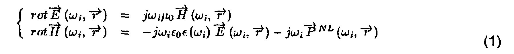
- E and H are respectively the electrical and induction fields. P NL represents the non-linear polarization and is defined by:
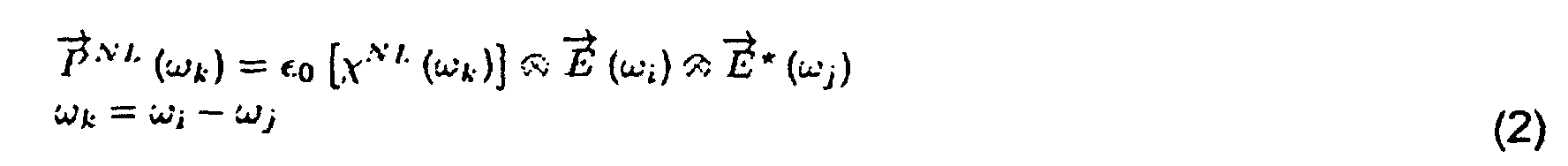
- ωi,j,k represent the different frequencies and χ the non linear suceptibility of the propagation medium. In order to solve equation (1), guided mode formalism is used, where the different fields are split on an orthogonal basis constituted by the local modes, as shown by the following equation:

- The fields with positive and negative superscript are respectively propagating and contra-propagating fields. E rad and H rad are the radiating parts of the electromagnetic field. Then, using the orthogonal properties of this decomposition, the variation of the amplitude of each wavelength is deduced from (1) and (3):

- The η coefficients represent the overlap of the three fields. Finally account is taken of the absorption of the propagation medium by introducing a complex value for Δk in the treatment of the system (4).
- In the preferred embodiment of the present invention, the
ground plane 16 is formed from a layer of gold deposited on a layer of titanium that is itself deposited on a layer ofsilica 17 serving as a support. - As shown in Figures 2, 5, 6 and 7 of the drawings, the microstrip
radio signal guide 15 extending parallel to and juxtaposed with theoptical guide 14 is connected with external radio signal wave-guides (one of which is shown at 18 in Figures 5 and 6 of WR15 type (standard wave-guides for 50 to 75 GHz radio frequencies). In the preferred embodiment of the invention the WR15 wave-guides extend perpendicularly to the length of the microstripradio signal guide 15 and theoptical guide 14 and parallel to theground plane 16. - Transition radio
signal guide elements ground plane 16 and present progressively varying cross sections to match the propagation characteristics of the microstrip with the WR15 wave-guides. More specifically, theguide elements microstrip 15 and the large end is of similar width to the corresponding width ('height') of the wave-guide WR15, such as 18. TheVivaldi antenna 21 is connected with the receiver circuit elements (for example, to a re-transmission circuit) while theVivaldi antenna 20 is connected to a n element presenting a matching load to themicrostrip 15, to ensure that it functions in balanced conditions. - The
microstrip element 15 traverses the small end of theVivaldi antennas optic layer microstrip 15 includesextensions microstrip 15 in radio signal coupling relationship with theoptical guide 14. The small ends of theVivaldi antennas optical guide 14. However, in an alternative embodiment of the invention shown in Figure 7, the small ends of theVivaldi antennas optical guide 14 and the microstrip-line 15 is entirely in line with theoptical guide 14 and in radio signal coupling relationship therewith. - In order to improve the frequency range of the device, radio
signal frequency resonators microstrip 15 andresonators Vivaldi antennas microstrip 15 and theVivaldi antenna - As shown in Figure 6, in the preferred embodiment of the invention, for a 60GHz radio carrier signal, the
Vivaldi antennas resonators resonators - In operation of the devices shown in Figure 2 and Figure 7, two optical signal components having frequencies that differ by an amount corresponding to the radio signal carrier frequency are applied to the optical input of the
optical guide 14. The two optical components interact in the second-order non-linear optical polarisation material of the electro-optical core 14. The close coupling of themicrostrip 15 andground plane 16 with theoptical guide 14 causes the radio frequency signals that result to be induced in the microstrip-line 15. Theline 15, together with itsextensions Vivaldi antennas guide 18 and the radio signal is received in the wave-guide. - In a modulator device such as 3 of similar construction, a radio signal propagated in the WR15 wave-guide with a single optical component propagated in the optical guide modulates the optical component so that at the output of the optical wave-guide two optical components are propagated.
- It is found that the output power of the electrical signal in the case of the detector device shown in the drawings is proportional to the square of the radio frequency, so that substantially higher efficiencies are obtained than in other devices whose efficiency reduces with frequency. The output of the radio signal is also proportional to the square of the interaction link and to the square of the input power of the optical signal: consequently the device is more efficient the more intense the optical signals but, concerning the interaction links, absorption of the optical signals in the optical guide limits the length of the optimum interaction link.
Claims (18)
- Apparatus for converting between optical and radio frequency signals comprising an optical guide (11 to 14) for propagating two optical signal components having frequencies that differ by an amount corresponding to a radio frequency and a first radio signal guide element (15, 16) for propagating a radio signal at said radio frequency, said first radio signal guide element being coupled with an interaction zone (14) of said optical guide comprising material in which interaction between said optical signal components and said radio signal occurs,
characterised in that the apparatus further comprises a second and third radio signal guide elements (20,21)(18) and a radio frequency signal resonator means (24 to 27), whereby said second radio signal guide element (20, 21) which is connected to said first radio signal guide element (15, 16) with said third radio signal guide element (18), said second radio signal guide element (20, 21) having a progressively varying cross-section adapting the propagation characteristics of said first (15, 16) and third (18) radio signal guide elements, and said radio frequency signal resonator means (24 to 27) are connected with said first and second radio signal guide elements. - Apparatus as claimed in claim 1, wherein said first radio signal guide element (15, 16) is in travelling-wave coupling with said interaction zone (14) of said optical guide.
- Apparatus as claimed in claim 2, wherein said interaction zone (14) and said travelling-wave coupling of said first radio signal guide element (15, 16) extend over a length of said optical guide at least as great as the wave-length of said radio signal in said first radio signal guide element (15, 16).
- Apparatus as claimed in any preceding claim, wherein the propagation velocities of said optical signal components in said interaction zone (14) and of said radio signal in said radio signal guide (15, 16) are substantially equal.
- Apparatus as claimed in any preceding claim, wherein said first radio signal guide element (15, 16) comprises an elongate member (15) of which at least part is juxtaposed with said interaction zone (14) and said resonator means comprises impedance-matching enlargements (24, 25) terminating each end of said elongate member (15).
- Apparatus as claimed in any preceding claim, wherein said resonator means comprises an impedance-matching enlargement (26, 27) terminating an end of said second radio signal guide element (20, 21).
- Apparatus as claimed in any preceding claim, wherein said second (20, 21) and third (18) radio signal guide elements extend transversely to said first radio signal guide element (15).
- Apparatus as claimed in any preceding claim, wherein said optical guide (11 to 14) comprises a ridge (14) formed in said interaction material at an interface with a material of different propagation characteristics (11), said interaction material having dimensions such that said optical signal components are channelled to propagate along said ridge (14).
- Apparatus as claimed in any preceding claim, wherein said first radio signal guide element (15, 16) comprises an electrically conductive strip (15) juxtaposed with and extending along said interaction zone (14) on one side thereof and a further electrically conductive element (16) juxtaposed with and extending along said interaction zone (14) on an opposite side thereof.
- Apparatus as claimed in claim 9, wherein said further electrically conductive element (16) also extends transversely to said interaction zone (14) and said second radio signal guide element (20, 21) comprises an opening of progressively varying width formed in said further electrically conductive element (16).
- Apparatus as claimed in claim 10, wherein said opening comprises a first part (20, 21) of progressively increasing width from a first end towards a second end, said first end being juxtaposed with said first radio signal guide element (15) in coupling relationship therewith, and said resonator means comprises an extension (26, 27) of said first part terminating said first end.
- Apparatus as claimed in claim 11, wherein said first part (20, 21) of said opening is generally trumpet-shaped.
- Apparatus as claimed in any preceding claim, wherein said third coupling means (18) comprises an elongate wave-guide having substantially parallel electrically conductive walls and said second radio signal guide element (20, 21) projects within said elongate wave-guide in coupling relationship therewith.
- Apparatus as claimed in any preceding claim, wherein said interaction material presents a second-order non-linear optical polarisation characteristic to the propagation of said optical signal.
- Apparatus as claimed in claim 14, wherein said interaction material comprises a dipolar material presenting non-centre-symmetric interaction characteristics to said optical signals.
- Apparatus as claimed in claim 14, wherein said interaction material includes a diazobenzene chromophore material having orientated electrical characteristics in a host matrix polymer material.
- An optical to radio frequency detector comprising apparatus as claimed in any preceding claim, means (1 to 10) for supplying said two optical signal components to said optical guide (11 to 14), and means coupled to said radio signal guide (15, 16) for receiving said radio signal.
- A modulator for modulating an optical signal comprising apparatus as claimed in any preceding claim, means (1, 2) for supplying said optical signal to said interaction zone (14), and means for supplying said radio signal to said radio signal guide (15, 16) so as to modulate said optical signal in said interaction zone (14) and generate said two optical signal components, which are propagated in said optical guide (11 to 14).
Priority Applications (11)
| Application Number | Priority Date | Filing Date | Title |
|---|---|---|---|
| AT02290319T ATE295971T1 (en) | 2002-02-08 | 2002-02-08 | CONVERSION BETWEEN OPTICAL AND HIGH FREQUENCY SIGNALS |
| EP02290319A EP1335239B1 (en) | 2002-02-08 | 2002-02-08 | Conversion between optical and radio frequency signals |
| DE60204210T DE60204210T2 (en) | 2002-02-08 | 2002-02-08 | Conversion between optical and high frequency signals |
| JP2003566607A JP4443932B2 (en) | 2002-02-08 | 2003-01-13 | Conversion between optical and radio frequency signals |
| CNB038033852A CN1322357C (en) | 2002-02-08 | 2003-01-13 | Conversion between optical and radio frequency signals |
| HK05109641.9A HK1075498B (en) | 2002-02-08 | 2003-01-13 | Conversion between optical and radio frequency signals |
| PCT/EP2003/000225 WO2003067314A1 (en) | 2002-02-08 | 2003-01-13 | Conversion between optical and radio frequency signals |
| KR1020047012296A KR100754759B1 (en) | 2002-02-08 | 2003-01-13 | Conversion between optical and radio frequency signals |
| AU2003244490A AU2003244490A1 (en) | 2002-02-08 | 2003-01-13 | Conversion between optical and radio frequency signals |
| US10/504,009 US7340178B2 (en) | 2002-02-08 | 2003-01-13 | Conversion between optical and radio frequency signals |
| TW092101475A TWI294223B (en) | 2002-02-08 | 2003-01-23 | Conversion between optical and radio frequency signals |
Applications Claiming Priority (1)
| Application Number | Priority Date | Filing Date | Title |
|---|---|---|---|
| EP02290319A EP1335239B1 (en) | 2002-02-08 | 2002-02-08 | Conversion between optical and radio frequency signals |
Publications (2)
| Publication Number | Publication Date |
|---|---|
| EP1335239A1 EP1335239A1 (en) | 2003-08-13 |
| EP1335239B1 true EP1335239B1 (en) | 2005-05-18 |
Family
ID=27589179
Family Applications (1)
| Application Number | Title | Priority Date | Filing Date |
|---|---|---|---|
| EP02290319A Expired - Lifetime EP1335239B1 (en) | 2002-02-08 | 2002-02-08 | Conversion between optical and radio frequency signals |
Country Status (10)
| Country | Link |
|---|---|
| US (1) | US7340178B2 (en) |
| EP (1) | EP1335239B1 (en) |
| JP (1) | JP4443932B2 (en) |
| KR (1) | KR100754759B1 (en) |
| CN (1) | CN1322357C (en) |
| AT (1) | ATE295971T1 (en) |
| AU (1) | AU2003244490A1 (en) |
| DE (1) | DE60204210T2 (en) |
| TW (1) | TWI294223B (en) |
| WO (1) | WO2003067314A1 (en) |
Families Citing this family (12)
| Publication number | Priority date | Publication date | Assignee | Title |
|---|---|---|---|---|
| EP1361683A1 (en) * | 2002-02-08 | 2003-11-12 | Motorola, Inc. | Optical to radio frequency detector |
| US7079722B2 (en) * | 2004-09-22 | 2006-07-18 | Maxentric Technologies Llc | Apparatus and method for transmitting electrical power through a transparent or substantially transparent medium |
| WO2007094944A2 (en) * | 2006-02-13 | 2007-08-23 | Battelle Memorial Institute | Millimeter and sub-millimeter wave detection |
| US7486247B2 (en) | 2006-02-13 | 2009-02-03 | Optimer Photonics, Inc. | Millimeter and sub-millimeter wave detection |
| US8901495B2 (en) * | 2010-03-30 | 2014-12-02 | Lawrence Livermore National Security, Llc. | Room-temperature quantum noise limited spectrometry and methods of the same |
| CN102157797A (en) * | 2011-03-08 | 2011-08-17 | 东南大学 | Broadband high-gain flat-plate Vivaldi antenna |
| US10468737B2 (en) * | 2017-12-30 | 2019-11-05 | Intel Corporation | Assembly and manufacturing friendly waveguide launchers |
| NL2021950B1 (en) * | 2018-11-07 | 2020-05-15 | Univ Delft Tech | Quantum wavelength converter between a microwave signal and an optical signal |
| CN111370987B (en) * | 2020-04-27 | 2025-08-26 | 中国电子科技集团公司第二十六研究所 | An acousto-optic Q-switch with a high damage threshold |
| EP3910414B1 (en) * | 2020-05-15 | 2023-08-02 | Miraex SA | Microwave-to-optical photon transducer |
| CN114865318B (en) * | 2022-05-17 | 2025-09-16 | 之江实验室 | Ultra-wideband high-gain terahertz antenna device easy to integrate with photodiode |
| WO2025232969A1 (en) * | 2024-05-08 | 2025-11-13 | Huawei Technologies Co., Ltd. | Antenna device |
Family Cites Families (8)
| Publication number | Priority date | Publication date | Assignee | Title |
|---|---|---|---|---|
| US5044725A (en) * | 1986-01-24 | 1991-09-03 | Hoechst Celanese Corp. | Polymeric thin film waveguide media |
| US5459800A (en) * | 1992-07-30 | 1995-10-17 | Matsushita Electric Industrial Co., Ltd. | Optical modulation device and method of driving the same |
| US5430568A (en) * | 1992-12-01 | 1995-07-04 | Scientific-Atlanta, Inc. | Optical communications system for transmitting information signals having different wavelengths over a same optical fiber |
| DE69415968T2 (en) * | 1993-03-31 | 1999-06-10 | British Telecomm | GENERATING OPTICAL SIGNALS WITH RF COMPONENTS |
| US5515463A (en) * | 1995-03-10 | 1996-05-07 | Hewlett-Packard Company | Multi-branch microwave line for electro-optical devices |
| US6558585B1 (en) * | 2000-11-02 | 2003-05-06 | Pacific Wave Industries, Inc. | Techniques for electrode poling of electro-optic polymers to eliminate poling induced optical loss and poling induced damage to electro-optic chromophores |
| US6987488B1 (en) * | 2001-02-16 | 2006-01-17 | The Texas A&M University System | Electromagnetic phase shifter using perturbation controlled by piezoelectric transducer and pha array antenna formed therefrom |
| US6711312B1 (en) * | 2002-12-20 | 2004-03-23 | General Electric Company | Integrated optoelectronic circuit and method of fabricating the same |
-
2002
- 2002-02-08 AT AT02290319T patent/ATE295971T1/en not_active IP Right Cessation
- 2002-02-08 DE DE60204210T patent/DE60204210T2/en not_active Expired - Fee Related
- 2002-02-08 EP EP02290319A patent/EP1335239B1/en not_active Expired - Lifetime
-
2003
- 2003-01-13 JP JP2003566607A patent/JP4443932B2/en not_active Expired - Fee Related
- 2003-01-13 CN CNB038033852A patent/CN1322357C/en not_active Expired - Fee Related
- 2003-01-13 AU AU2003244490A patent/AU2003244490A1/en not_active Abandoned
- 2003-01-13 US US10/504,009 patent/US7340178B2/en not_active Expired - Lifetime
- 2003-01-13 WO PCT/EP2003/000225 patent/WO2003067314A1/en not_active Ceased
- 2003-01-13 KR KR1020047012296A patent/KR100754759B1/en not_active Expired - Fee Related
- 2003-01-23 TW TW092101475A patent/TWI294223B/en not_active IP Right Cessation
Also Published As
| Publication number | Publication date |
|---|---|
| KR20060066569A (en) | 2006-06-16 |
| ATE295971T1 (en) | 2005-06-15 |
| TW200303657A (en) | 2003-09-01 |
| CN1322357C (en) | 2007-06-20 |
| TWI294223B (en) | 2008-03-01 |
| JP4443932B2 (en) | 2010-03-31 |
| DE60204210D1 (en) | 2005-06-23 |
| JP2005517208A (en) | 2005-06-09 |
| HK1075498A1 (en) | 2005-12-16 |
| WO2003067314A1 (en) | 2003-08-14 |
| US20050152631A1 (en) | 2005-07-14 |
| DE60204210T2 (en) | 2005-10-13 |
| AU2003244490A1 (en) | 2003-09-02 |
| EP1335239A1 (en) | 2003-08-13 |
| US7340178B2 (en) | 2008-03-04 |
| KR100754759B1 (en) | 2007-09-04 |
| CN1628259A (en) | 2005-06-15 |
Similar Documents
| Publication | Publication Date | Title |
|---|---|---|
| US5208697A (en) | Microwave frequency range electro-optic modulator with efficient input coupling and smooth wideband frequency response | |
| US5644664A (en) | Fiber optic digital transmission system | |
| US20220052760A1 (en) | Electronic device for converting a wireless signal into at least one modulated optical signal | |
| CN1152980A (en) | Generation of radio frequency modulated optical radiation | |
| EP1335239B1 (en) | Conversion between optical and radio frequency signals | |
| US7016554B2 (en) | Optical modulator | |
| Salamin et al. | 300 GHz plasmonic mixer | |
| US7877015B2 (en) | Optical to radio frequency detector | |
| Jäger | 1 Microwave Photonics | |
| Loi et al. | Low-loss 1.3-μm MQW electroabsorption modulators for high-linearity analog optical links | |
| Maury et al. | Remote upconversion in microwave fiber optic links employing an unbalanced Mach-Zehnder interferometer | |
| Mortazy et al. | Mode coupling between substrate integrated waveguide and coplanar waveguide for traveling-wave electrooptical modulator | |
| CN114389704A (en) | Microwave photonic filter based on MZI-MRR structure | |
| HK1075498B (en) | Conversion between optical and radio frequency signals | |
| Wijayanto et al. | Metamaterial antenna integrated to LiNbO3 optical modulator for millimeter-wave-photonic links | |
| Devaux et al. | Optical processing with electroabsorption modulators | |
| Burla et al. | Plasmonic modulators for microwave photonics applications | |
| Lu et al. | A Broadband Lithium Tantalate-on-Silicon Nitride Heterogeneous Modulator for Optical and Terahertz Communications and Radar Sensing | |
| CN118785023A (en) | Wired/wireless hybrid optical access system and method based on upper/lower sideband modulation | |
| JP3225113B2 (en) | Frequency mixer equipment | |
| Knoesen et al. | High-bandwidth polymer in-line fiber modulator | |
| Akaike | Trends of research on microwaves/optics in Japan | |
| JPH077322A (en) | Slot antenna system | |
| Mcelhanon et al. | Fiber Optic Digital Transmission System. | |
| Penard et al. | Intensity modulation of LiNbO3 electro-optic modulator by free-space radiation coupling |
Legal Events
| Date | Code | Title | Description |
|---|---|---|---|
| PUAI | Public reference made under article 153(3) epc to a published international application that has entered the european phase |
Free format text: ORIGINAL CODE: 0009012 |
|
| AK | Designated contracting states |
Designated state(s): AT BE CH CY DE DK ES FI FR GB GR IE IT LI LU MC NL PT SE TR |
|
| AX | Request for extension of the european patent |
Extension state: AL LT LV MK RO SI |
|
| 17P | Request for examination filed |
Effective date: 20040213 |
|
| GRAP | Despatch of communication of intention to grant a patent |
Free format text: ORIGINAL CODE: EPIDOSNIGR1 |
|
| RAP1 | Party data changed (applicant data changed or rights of an application transferred) |
Owner name: FREESCALE SEMICONDUCTOR, INC. |
|
| GRAS | Grant fee paid |
Free format text: ORIGINAL CODE: EPIDOSNIGR3 |
|
| GRAA | (expected) grant |
Free format text: ORIGINAL CODE: 0009210 |
|
| AKX | Designation fees paid |
Designated state(s): AT BE CH CY DE DK ES FI FR GB GR IE IT LI LU MC NL PT SE TR |
|
| AK | Designated contracting states |
Kind code of ref document: B1 Designated state(s): AT BE CH CY DE DK ES FI FR GB GR IE IT LI LU MC NL PT SE TR |
|
| PG25 | Lapsed in a contracting state [announced via postgrant information from national office to epo] |
Ref country code: NL Free format text: LAPSE BECAUSE OF FAILURE TO SUBMIT A TRANSLATION OF THE DESCRIPTION OR TO PAY THE FEE WITHIN THE PRESCRIBED TIME-LIMIT Effective date: 20050518 Ref country code: AT Free format text: LAPSE BECAUSE OF FAILURE TO SUBMIT A TRANSLATION OF THE DESCRIPTION OR TO PAY THE FEE WITHIN THE PRESCRIBED TIME-LIMIT Effective date: 20050518 Ref country code: LI Free format text: LAPSE BECAUSE OF FAILURE TO SUBMIT A TRANSLATION OF THE DESCRIPTION OR TO PAY THE FEE WITHIN THE PRESCRIBED TIME-LIMIT Effective date: 20050518 Ref country code: TR Free format text: LAPSE BECAUSE OF FAILURE TO SUBMIT A TRANSLATION OF THE DESCRIPTION OR TO PAY THE FEE WITHIN THE PRESCRIBED TIME-LIMIT Effective date: 20050518 Ref country code: FI Free format text: LAPSE BECAUSE OF FAILURE TO SUBMIT A TRANSLATION OF THE DESCRIPTION OR TO PAY THE FEE WITHIN THE PRESCRIBED TIME-LIMIT Effective date: 20050518 Ref country code: CH Free format text: LAPSE BECAUSE OF FAILURE TO SUBMIT A TRANSLATION OF THE DESCRIPTION OR TO PAY THE FEE WITHIN THE PRESCRIBED TIME-LIMIT Effective date: 20050518 Ref country code: BE Free format text: LAPSE BECAUSE OF FAILURE TO SUBMIT A TRANSLATION OF THE DESCRIPTION OR TO PAY THE FEE WITHIN THE PRESCRIBED TIME-LIMIT Effective date: 20050518 |
|
| REG | Reference to a national code |
Ref country code: GB Ref legal event code: FG4D |
|
| REG | Reference to a national code |
Ref country code: CH Ref legal event code: EP |
|
| REG | Reference to a national code |
Ref country code: IE Ref legal event code: FG4D |
|
| REF | Corresponds to: |
Ref document number: 60204210 Country of ref document: DE Date of ref document: 20050623 Kind code of ref document: P |
|
| PG25 | Lapsed in a contracting state [announced via postgrant information from national office to epo] |
Ref country code: DK Free format text: LAPSE BECAUSE OF FAILURE TO SUBMIT A TRANSLATION OF THE DESCRIPTION OR TO PAY THE FEE WITHIN THE PRESCRIBED TIME-LIMIT Effective date: 20050818 Ref country code: SE Free format text: LAPSE BECAUSE OF FAILURE TO SUBMIT A TRANSLATION OF THE DESCRIPTION OR TO PAY THE FEE WITHIN THE PRESCRIBED TIME-LIMIT Effective date: 20050818 Ref country code: GR Free format text: LAPSE BECAUSE OF FAILURE TO SUBMIT A TRANSLATION OF THE DESCRIPTION OR TO PAY THE FEE WITHIN THE PRESCRIBED TIME-LIMIT Effective date: 20050818 |
|
| PG25 | Lapsed in a contracting state [announced via postgrant information from national office to epo] |
Ref country code: ES Free format text: LAPSE BECAUSE OF FAILURE TO SUBMIT A TRANSLATION OF THE DESCRIPTION OR TO PAY THE FEE WITHIN THE PRESCRIBED TIME-LIMIT Effective date: 20050829 |
|
| PG25 | Lapsed in a contracting state [announced via postgrant information from national office to epo] |
Ref country code: PT Free format text: LAPSE BECAUSE OF FAILURE TO SUBMIT A TRANSLATION OF THE DESCRIPTION OR TO PAY THE FEE WITHIN THE PRESCRIBED TIME-LIMIT Effective date: 20051024 |
|
| REG | Reference to a national code |
Ref country code: CH Ref legal event code: PL |
|
| NLV1 | Nl: lapsed or annulled due to failure to fulfill the requirements of art. 29p and 29m of the patents act | ||
| PG25 | Lapsed in a contracting state [announced via postgrant information from national office to epo] |
Ref country code: IE Free format text: LAPSE BECAUSE OF NON-PAYMENT OF DUE FEES Effective date: 20060208 |
|
| PG25 | Lapsed in a contracting state [announced via postgrant information from national office to epo] |
Ref country code: LU Free format text: LAPSE BECAUSE OF NON-PAYMENT OF DUE FEES Effective date: 20060228 Ref country code: MC Free format text: LAPSE BECAUSE OF NON-PAYMENT OF DUE FEES Effective date: 20060228 |
|
| PGFP | Annual fee paid to national office [announced via postgrant information from national office to epo] |
Ref country code: IT Payment date: 20060228 Year of fee payment: 5 |
|
| ET | Fr: translation filed | ||
| PLBE | No opposition filed within time limit |
Free format text: ORIGINAL CODE: 0009261 |
|
| STAA | Information on the status of an ep patent application or granted ep patent |
Free format text: STATUS: NO OPPOSITION FILED WITHIN TIME LIMIT |
|
| 26N | No opposition filed |
Effective date: 20060221 |
|
| REG | Reference to a national code |
Ref country code: IE Ref legal event code: MM4A |
|
| PGFP | Annual fee paid to national office [announced via postgrant information from national office to epo] |
Ref country code: GB Payment date: 20070105 Year of fee payment: 6 |
|
| PGFP | Annual fee paid to national office [announced via postgrant information from national office to epo] |
Ref country code: DE Payment date: 20070228 Year of fee payment: 6 |
|
| PGFP | Annual fee paid to national office [announced via postgrant information from national office to epo] |
Ref country code: FR Payment date: 20070201 Year of fee payment: 6 |
|
| GBPC | Gb: european patent ceased through non-payment of renewal fee |
Effective date: 20080208 |
|
| PG25 | Lapsed in a contracting state [announced via postgrant information from national office to epo] |
Ref country code: CY Free format text: LAPSE BECAUSE OF FAILURE TO SUBMIT A TRANSLATION OF THE DESCRIPTION OR TO PAY THE FEE WITHIN THE PRESCRIBED TIME-LIMIT Effective date: 20050518 |
|
| REG | Reference to a national code |
Ref country code: FR Ref legal event code: ST Effective date: 20081031 |
|
| PG25 | Lapsed in a contracting state [announced via postgrant information from national office to epo] |
Ref country code: DE Free format text: LAPSE BECAUSE OF NON-PAYMENT OF DUE FEES Effective date: 20080902 |
|
| PG25 | Lapsed in a contracting state [announced via postgrant information from national office to epo] |
Ref country code: FR Free format text: LAPSE BECAUSE OF NON-PAYMENT OF DUE FEES Effective date: 20080229 |
|
| PG25 | Lapsed in a contracting state [announced via postgrant information from national office to epo] |
Ref country code: GB Free format text: LAPSE BECAUSE OF NON-PAYMENT OF DUE FEES Effective date: 20080208 |
|
| PG25 | Lapsed in a contracting state [announced via postgrant information from national office to epo] |
Ref country code: IT Free format text: LAPSE BECAUSE OF NON-PAYMENT OF DUE FEES Effective date: 20070208 |