EP1335192A1 - Nanotube, nanothermometer and method for producing the same - Google Patents
Nanotube, nanothermometer and method for producing the same Download PDFInfo
- Publication number
- EP1335192A1 EP1335192A1 EP03250689A EP03250689A EP1335192A1 EP 1335192 A1 EP1335192 A1 EP 1335192A1 EP 03250689 A EP03250689 A EP 03250689A EP 03250689 A EP03250689 A EP 03250689A EP 1335192 A1 EP1335192 A1 EP 1335192A1
- Authority
- EP
- European Patent Office
- Prior art keywords
- temperature
- producing
- nano thermometer
- powder
- nano
- Prior art date
- Legal status (The legal status is an assumption and is not a legal conclusion. Google has not performed a legal analysis and makes no representation as to the accuracy of the status listed.)
- Granted
Links
- 238000004519 manufacturing process Methods 0.000 title claims abstract description 20
- 239000002071 nanotube Substances 0.000 title claims description 9
- OKTJSMMVPCPJKN-UHFFFAOYSA-N Carbon Chemical compound [C] OKTJSMMVPCPJKN-UHFFFAOYSA-N 0.000 claims abstract description 60
- 239000002041 carbon nanotube Substances 0.000 claims abstract description 29
- 229910021393 carbon nanotube Inorganic materials 0.000 claims abstract description 28
- 238000010438 heat treatment Methods 0.000 claims abstract description 17
- QZQVBEXLDFYHSR-UHFFFAOYSA-N gallium(III) oxide Inorganic materials O=[Ga]O[Ga]=O QZQVBEXLDFYHSR-UHFFFAOYSA-N 0.000 claims abstract description 13
- 238000000034 method Methods 0.000 claims abstract description 12
- 239000000843 powder Substances 0.000 claims abstract description 12
- 229910052733 gallium Inorganic materials 0.000 claims abstract description 11
- 239000011261 inert gas Substances 0.000 claims abstract description 10
- GYHNNYVSQQEPJS-UHFFFAOYSA-N Gallium Chemical compound [Ga] GYHNNYVSQQEPJS-UHFFFAOYSA-N 0.000 claims abstract description 9
- 238000005259 measurement Methods 0.000 claims abstract description 8
- 239000011812 mixed powder Substances 0.000 claims abstract description 6
- 230000007613 environmental effect Effects 0.000 claims abstract description 5
- 229910052799 carbon Inorganic materials 0.000 claims description 8
- 238000006243 chemical reaction Methods 0.000 claims description 8
- IJGRMHOSHXDMSA-UHFFFAOYSA-N Atomic nitrogen Chemical compound N#N IJGRMHOSHXDMSA-UHFFFAOYSA-N 0.000 claims description 3
- 229910001873 dinitrogen Inorganic materials 0.000 claims description 3
- 238000009529 body temperature measurement Methods 0.000 abstract description 8
- 229910002804 graphite Inorganic materials 0.000 description 8
- 239000010439 graphite Substances 0.000 description 8
- 239000000463 material Substances 0.000 description 8
- 239000007788 liquid Substances 0.000 description 6
- 229910005224 Ga2O Inorganic materials 0.000 description 4
- 238000011160 research Methods 0.000 description 4
- 230000015572 biosynthetic process Effects 0.000 description 3
- 230000007423 decrease Effects 0.000 description 3
- 239000000376 reactant Substances 0.000 description 3
- 239000007787 solid Substances 0.000 description 3
- 238000004458 analytical method Methods 0.000 description 2
- 238000013459 approach Methods 0.000 description 2
- 230000005540 biological transmission Effects 0.000 description 2
- 238000004364 calculation method Methods 0.000 description 2
- 238000000151 deposition Methods 0.000 description 2
- 230000008021 deposition Effects 0.000 description 2
- 238000000724 energy-dispersive X-ray spectrum Methods 0.000 description 2
- 239000007789 gas Substances 0.000 description 2
- 238000000024 high-resolution transmission electron micrograph Methods 0.000 description 2
- 238000002173 high-resolution transmission electron microscopy Methods 0.000 description 2
- 239000011796 hollow space material Substances 0.000 description 2
- 229910052751 metal Inorganic materials 0.000 description 2
- 239000002184 metal Substances 0.000 description 2
- 239000002994 raw material Substances 0.000 description 2
- UFHFLCQGNIYNRP-UHFFFAOYSA-N Hydrogen Chemical compound [H][H] UFHFLCQGNIYNRP-UHFFFAOYSA-N 0.000 description 1
- 230000008602 contraction Effects 0.000 description 1
- 230000003247 decreasing effect Effects 0.000 description 1
- 238000004146 energy storage Methods 0.000 description 1
- 238000002474 experimental method Methods 0.000 description 1
- 230000005669 field effect Effects 0.000 description 1
- 229910052739 hydrogen Inorganic materials 0.000 description 1
- 239000001257 hydrogen Substances 0.000 description 1
- QSHDDOUJBYECFT-UHFFFAOYSA-N mercury Chemical compound [Hg] QSHDDOUJBYECFT-UHFFFAOYSA-N 0.000 description 1
- 229910052753 mercury Inorganic materials 0.000 description 1
- 238000011946 reduction process Methods 0.000 description 1
- 239000000523 sample Substances 0.000 description 1
- 238000007711 solidification Methods 0.000 description 1
- 230000008023 solidification Effects 0.000 description 1
- 238000003786 synthesis reaction Methods 0.000 description 1
- 238000007704 wet chemistry method Methods 0.000 description 1
Images


Classifications
-
- B—PERFORMING OPERATIONS; TRANSPORTING
- B82—NANOTECHNOLOGY
- B82Y—SPECIFIC USES OR APPLICATIONS OF NANOSTRUCTURES; MEASUREMENT OR ANALYSIS OF NANOSTRUCTURES; MANUFACTURE OR TREATMENT OF NANOSTRUCTURES
- B82Y30/00—Nanotechnology for materials or surface science, e.g. nanocomposites
-
- G—PHYSICS
- G01—MEASURING; TESTING
- G01K—MEASURING TEMPERATURE; MEASURING QUANTITY OF HEAT; THERMALLY-SENSITIVE ELEMENTS NOT OTHERWISE PROVIDED FOR
- G01K5/00—Measuring temperature based on the expansion or contraction of a material
- G01K5/02—Measuring temperature based on the expansion or contraction of a material the material being a liquid
- G01K5/04—Details
- G01K5/08—Capillary tubes
-
- B—PERFORMING OPERATIONS; TRANSPORTING
- B82—NANOTECHNOLOGY
- B82Y—SPECIFIC USES OR APPLICATIONS OF NANOSTRUCTURES; MEASUREMENT OR ANALYSIS OF NANOSTRUCTURES; MANUFACTURE OR TREATMENT OF NANOSTRUCTURES
- B82Y15/00—Nanotechnology for interacting, sensing or actuating, e.g. quantum dots as markers in protein assays or molecular motors
-
- Y—GENERAL TAGGING OF NEW TECHNOLOGICAL DEVELOPMENTS; GENERAL TAGGING OF CROSS-SECTIONAL TECHNOLOGIES SPANNING OVER SEVERAL SECTIONS OF THE IPC; TECHNICAL SUBJECTS COVERED BY FORMER USPC CROSS-REFERENCE ART COLLECTIONS [XRACs] AND DIGESTS
- Y10—TECHNICAL SUBJECTS COVERED BY FORMER USPC
- Y10S—TECHNICAL SUBJECTS COVERED BY FORMER USPC CROSS-REFERENCE ART COLLECTIONS [XRACs] AND DIGESTS
- Y10S977/00—Nanotechnology
- Y10S977/70—Nanostructure
- Y10S977/762—Nanowire or quantum wire, i.e. axially elongated structure having two dimensions of 100 nm or less
-
- Y—GENERAL TAGGING OF NEW TECHNOLOGICAL DEVELOPMENTS; GENERAL TAGGING OF CROSS-SECTIONAL TECHNOLOGIES SPANNING OVER SEVERAL SECTIONS OF THE IPC; TECHNICAL SUBJECTS COVERED BY FORMER USPC CROSS-REFERENCE ART COLLECTIONS [XRACs] AND DIGESTS
- Y10—TECHNICAL SUBJECTS COVERED BY FORMER USPC
- Y10S—TECHNICAL SUBJECTS COVERED BY FORMER USPC CROSS-REFERENCE ART COLLECTIONS [XRACs] AND DIGESTS
- Y10S977/00—Nanotechnology
- Y10S977/70—Nanostructure
- Y10S977/811—Of specified metal oxide composition, e.g. conducting or semiconducting compositions such as ITO, ZnOx
-
- Y—GENERAL TAGGING OF NEW TECHNOLOGICAL DEVELOPMENTS; GENERAL TAGGING OF CROSS-SECTIONAL TECHNOLOGIES SPANNING OVER SEVERAL SECTIONS OF THE IPC; TECHNICAL SUBJECTS COVERED BY FORMER USPC CROSS-REFERENCE ART COLLECTIONS [XRACs] AND DIGESTS
- Y10—TECHNICAL SUBJECTS COVERED BY FORMER USPC
- Y10S—TECHNICAL SUBJECTS COVERED BY FORMER USPC CROSS-REFERENCE ART COLLECTIONS [XRACs] AND DIGESTS
- Y10S977/00—Nanotechnology
- Y10S977/70—Nanostructure
- Y10S977/832—Nanostructure having specified property, e.g. lattice-constant, thermal expansion coefficient
- Y10S977/833—Thermal property of nanomaterial, e.g. thermally conducting/insulating or exhibiting peltier or seebeck effect
-
- Y—GENERAL TAGGING OF NEW TECHNOLOGICAL DEVELOPMENTS; GENERAL TAGGING OF CROSS-SECTIONAL TECHNOLOGIES SPANNING OVER SEVERAL SECTIONS OF THE IPC; TECHNICAL SUBJECTS COVERED BY FORMER USPC CROSS-REFERENCE ART COLLECTIONS [XRACs] AND DIGESTS
- Y10—TECHNICAL SUBJECTS COVERED BY FORMER USPC
- Y10S—TECHNICAL SUBJECTS COVERED BY FORMER USPC CROSS-REFERENCE ART COLLECTIONS [XRACs] AND DIGESTS
- Y10S977/00—Nanotechnology
- Y10S977/902—Specified use of nanostructure
- Y10S977/932—Specified use of nanostructure for electronic or optoelectronic application
- Y10S977/953—Detector using nanostructure
- Y10S977/955—Of thermal property
Definitions
- the present invention relates a nanotube, a nano thermometer and a method for producing the same. More particularly, the present invention relates to a nanotube, and novel nano thermometer using the nanotube, which can use for temperature measurement of a wide temperature range, in a micrometer size environment, and a method for producing the same.
- CNTs carbon nanotubes
- they can serve as field-effect devices, probe-tips for scanning probe microscope, superconducting material, high-sensitivity microbalances, structural materials, tiny tweezers for nanoscale manipulation, gas detectors and hydrogen energy storage devices etc.
- thermometers designed for a macroscopic environment are no longer appropriate for a micrometer-size environment, and a nano thermometer, which can perform temperature measurement of micrometer size environment, is needed.
- thermometer had the comparatively narrow temperature range which can be measured, and some thermometers needed to be prepared for every measurement temperature when a wide range temperature was measured.
- the object is to provide a solution to the above-mentioned problems of the conventional thermometer, and to provide a novel nano thermometer, which enables temperature measurement of a wide temperature range in a micrometer size environment, and a method for producing the same.
- Figure 1 shows the morphology of a wire indicated by the arrow, (b) shows the morphology of that the wire is wrapped by a thin layer on its round tip and body, (c) shows the HRTEM image of the thin wrapping layer, (d) shows an EDS spectrum from the region in (c).
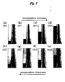
- Figure 2 shows the morphologies of the Ga tip when the temperature increases from 18°C (a), via 58°C (b) and 294°C (c), to 490°C (d), as well as the morphologies when the temperature decreases from 490°C (d) , via 330°C (e), 170°C (f) and 45°C (g), to 22°C (h).
- the present invention firstly provides, as a means to solve the above-mentioned problems, a nano thermometer, comprising a carbon nanotube filled with a continuous columnar gallium, which enables measurement of environmental temperature by length change of the columnar gallium.
- the present invention secondly provides a nano thermometer, having length of 1-10 ⁇ m and diameters of 40-150 nm.
- the invention thirdly provides a nano thermometer, which enables measurement of the temperature of the range of at least 50 to 500°C.
- the present invention fourthly provides a nano thermometer, whose error is within 0.25 °C.
- the present invention fifthly provides a nanotube, comprising a carbon nanotube filled with a columnar gallium.
- the present invention sixthly provide a method for producing a nano thermometer, said method comprising mixing Ga 2 O 3 powder and carbon powder uniformly, performing heat treatment for this mixed powder at a temperature of 966 °C or more under an inert gas flow to vaporize, and making a reaction at a temperature of 835°C or less.
- the present invention seventhly provides a method for producing a nano thermometer, wherein a weight ratio of Ga 2 O 3 powder to carbon powder is 7.8:1.
- the present invention eighthly provides a method for producing a nano thermometer, wherein carbon powder is an amorphous active carbon.
- the present invention ninthly provides a method for producing a nano thermometer, wherein inert gas is nitrogen gas, and tenthly provides a method for producing a nano thermometer, wherein heat treatment is performed using a vertical radio-frequency furnace. Also, the present invention eleventhly provides a method for producing a nano thermometer, wherein heat treatment is performed for 1 hour or more at a temperature of 1300 to 1400°C.
- the present inventions provide a nano thermometer which can also be considered as novel potential application of a carbon nanotube (CNT) . That is, the nanotube of the present invention comprising a carbon nanotube filled with a columnar gallium (Ga). And the nano thermometer of the present invention comprising a CNT filled with a continuous columnar Ga, which enables measurement of environmental temperature by length change of the columnar Ga. This potential application is based on the expansion characteristic of Ga in the inside of a CNT. In the nano thermometer of the present invention, since the hollowcylinder of CNT is filled with Ga, Ga has the form of as a continuous column.
- the reason why Ga rather than another metal is chosen as the filling material is that Ga has one of the longest liquid ranges of any metal, i.e. 29.78-2,403°C, and has a low vapor pressure even at high temperatures, which makes it suitable for use in a wide-temperature-range thermometer. Therefore, the nano thermometer of the present invention has a potential wide measuring range due to the wide liquid range of Ga, 29.78 to 2,403°C, which is much wider than that of Hg, -38.87 to 356.58°C.
- thermometer the length of the columnar Ga increases linearly with increasing temperature in the temperature range of 50 to 500°C. Therefore, with the nano thermometer of the present invention, environmental temperature can be measured from the length of Ga simpler and correctly in the temperature range of 50 to 500°C.
- the present nano thermometer even more surprising, can realize a very highly precise nano thermometer within 0.25°C of errors .
- the nano thermometer of the present invention uses the detailed structure of a CNT, the very small thermometer of a micrometer-size is realized.
- the nano thermometer having length of 1-10 ⁇ m and diameters of 40-150 nm is realized.
- Ga can be made to extend up to about 8 mm in CNT.
- the nano thermometer of the present invention can play an important role in various researches involving temperature measurement of a wide temperature range in micrometer environment.
- the nano thermometer of the present invention is producible by a method of present invention as follows. That is, in the method of the present invention, it is made to manufacture a nano thermometer by mixing Ga 2 O 3 powder and carbon powder uniformly, performing heat treatment for this mixed powder at a temperature of 966°C or more under an inert gas flow to vaporize, and making a reaction at a temperature of 835°C or less.
- carbon powder can be used as raw material of the CNT part which constitutes a nano thermometer.
- carbon powder carbon powder of comparatively high purity, for example 90% or more of purity, can be used.
- Ga 2 O 3 powder can be used as raw material of the columnar Ga filling in the CNT.
- a weight ratio of Ga 2 O 3 powder to carbon powder can be adjusted in the range of about 7:1 to 8:1, and is 7.8:1 more preferably.
- Ga 2 O 3 powder and carbon powder are mixed uniformly, and are performed heat treatment at a temperature of 966°C or more under an inert gas flow.
- the mixed powder of Ga 2 O 3 and carbon is vaporizable at a temperature of 966°C or more, it is more desirable that heat treatment is performed at the temperature range from 1200 to 1400°C.
- an inert gas is desirable nitrogen gas.
- the vapors are carried by the inert gas flow, and they can react at the temperature of 835°C or less and are deposited.
- a vertical radio-frequency furnace can be used in the method of the present invention. If a susceptor of the vertical radio-frequency furnace has one bottom inlet pipe and one top outlet pipe of the inert gas flow, the nano thermometer of the present invention can be obtained on the inner surface of the top outlet pipe as depositions, for example.
- heat treatment can be performed at a temperature range from 1200 to 1400°C as above-mentioned. More specifically, a heat treatment of 1 hour or more at the temperature from 1300 to 1400°C can be made as a rough standard.
- the nano thermometer was produced using the vertical radio-frequency furnace as described by the reference; Golberg, G. et al. Large-scale synthesis and HRTEM analysis of single - walled B- and N-doped carbon nanotube bundles. Carbon 38, 2017-2027 (2000).
- the reactant was a homogenous mixed powder of Ga 2 O 3 and pure amorphous active carbon (AAC) in the weight ratio 7.8:1.
- the graphite susceptor of the vertical radio-frequency furnace had one bottom inlet pipe and one top outlet pipe made of 99.99% purity graphite. Pure N 2 gas flow was introduced into the furnace .
- Heat treatment at 1,360°C for 2 hours was performed for the reactant. After the heat treatment, the reactant in the graphite crucible disappeared, while some materials were found to have deposited on the inner surface of the top outlet graphite pipe. In the deposition zone, the temperature was measured to be ⁇ 800°C.
- FIG. 1(a) shows several 1-dimensional (1D) nanoscale wires of the deposited materials, which have lengths of 1-10 ⁇ m and diameters of 40-150 nm. The bar at the lower right corner corresponds to 1 ⁇ m. The wire indicated by the arrow was analyzed carefully.
- the HRTEM image in Fig. 1(c) shows that this thin layer is carbon.
- FIG. 1(d) An EDS spectrum from the region in (c).
- the horizontal axis is Energy axis, while the vertical is Intensity in arbitrary unit.
- the peaks of C-K ⁇ (0.28 keV), Ga-L ⁇ (1.10 keV), Ga-K ⁇ (9.24keV) and Ga-K ⁇ (10.26keV) are shown, the Cu peak was originated from the Cu TEM grid. That is, it shows that the wire contains Ga and C.
- the indicated wire is a CNT filled with Ga. From the left to the right of the CNT shown in (a) , there are round tips, a long columnar Ga, a hollow space beside the arrowhead, a short columnar Ga and another hollow space. In (b), the length and outer diameter d o of the CNT are 9,180 nm and 85 nm, while the length L 0 and diameter d 1 of the longer columnar Ga are 7,560 nm and 75 nm, respectively.
- the round tip keeps its shape and size when the temperature changes.
- the transmission electron microscope (TEM) specimen of the deposited materials was heated in the microscope using a Gatan heating holder and its twin heating system (Hot Stage Powder Supply, Model 628-0500).
- the position of the Ga tip-level of the longer columnar Ga vs temperature was investigated in the range 18-500°C.
- the Ga tip-level rises, as shown in Figs. 2(a), (b) , (c) and (d).
- the Ga tip-level goes down when the temperature decreases, as shown in Figs. 2(e), (f), (g) and (h) .
- the Ga tip-level goes up when the temperature increases, while it goes down when the temperature decreases.
- the bar in (a) corresponds to 85 nm.
- the height of the Ga tip-level vs temperature can be plotted as shown in Fig. 3, where the lines which connect a black circles and a black triangles correspond to the increase process and reduction process of temperature, respectively.
- the changes of the complete length and the inner-diameter of the CNT were measured and estimated to be ⁇ -1 ⁇ due to the very small linear expansion coefficient of graphite ( ⁇ -1 ⁇ 10 -6 /°C along a axis in the range of 20-500°C). Therefore, it is believed that the influence of the expansion of the CNT on the Ga tip-level position can be neglected and the height vs temperature is dominated by the volumetric change of the longer columnar Ga related to the environment temperature.
- v t v 0 ( 1 + a ⁇ t + b ⁇ t 2 + c ⁇ t 3 )
- v t and v 0 are the liquid volumes at temperature t and t 0 , respectively
- ⁇ t t - t 0
- a, b and c are the coefficient of cubical expansion.
- the coefficients b and c of Ga can be regarded as zero in the range 50-500°C.
- Figure 3 shows that the height of the Ga tip-level is reproducible and linearly changes in the range 50-500°C.
- the characteristic in the range 20-50°C is complicated and may be related to a liquefaction (or solidification) process when increasing (or decreasing) the temperature.
- the CNT filled with a long continuous columnar Ga can be used as a thermometer in the range of at least 50-500°C.
- v 0 is the volume of a continuous columnar Ga at temperature t 0
- ⁇ H is the difference between the heights of the Ga tip-level at temperatures t and t 0
- the columnar Ga should have a large volume v 0 and a small diameter d 1 .
- ⁇ H and t are in units nm and °C, respectively.
- the resolution of a microscope is ⁇ 0.2 nm
- the accuracy of the temperature measurement can reach ⁇ 0.25°C.
- the nano thermometer of the present invention can be used for the measurement in a micrometer-size environment.
- many researches have stepped into a size of at least micrometer. Therefore, the four kinds of thermometers designed for a macroscopic environment are no longer appropriate for a micrometer-size environment.
- the nano thermometer of the present invention could play an important role in various researches involving a temperature measurement of micrometer-size environment.
- the present kind of nano thermometer filled with Ga has a potential wide measuring range due to the wide liquid range (29.78-2,403°C) of Ga, which is much wider than that (-38.87-356.58°C) of Hg.
- the method for producing the CNTs filled with a long columnar Ga belongs to the second approach.
- the growth of the Ga filling CNTs may involve two chemical reactions. At a temperature above 966°C, Ga 2 O and CO vapours can be generated by the reaction; Ga 2 O 3 (solid) + 2C(solid) ⁇ Ga 2 O(vapour) + 2CO(vapour), between Ga 2 O 3 and AAC powder in the graphite crucible.
- n is estimated to be ⁇ 1.
- the present invention provides novel nano thermometer, which can use for temperature measurement of a wide temperature range, in a micrometer size environment, and a method for producing the same.
Landscapes
- Chemical & Material Sciences (AREA)
- Engineering & Computer Science (AREA)
- Nanotechnology (AREA)
- Physics & Mathematics (AREA)
- General Physics & Mathematics (AREA)
- Crystallography & Structural Chemistry (AREA)
- Materials Engineering (AREA)
- Condensed Matter Physics & Semiconductors (AREA)
- Composite Materials (AREA)
- Health & Medical Sciences (AREA)
- Life Sciences & Earth Sciences (AREA)
- General Health & Medical Sciences (AREA)
- Molecular Biology (AREA)
- Carbon And Carbon Compounds (AREA)
- Measuring Temperature Or Quantity Of Heat (AREA)
Abstract
Description
- The present invention relates a nanotube, a nano thermometer and a method for producing the same. More particularly, the present invention relates to a nanotube, and novel nano thermometer using the nanotube, which can use for temperature measurement of a wide temperature range, in a micrometer size environment, and a method for producing the same.
- As a result of many researchers' having studied of many about carbon nanotubes (CNTs) since its discovery in 1991, CNTs found those uses in many fields. For example, they can serve as field-effect devices, probe-tips for scanning probe microscope, superconducting material, high-sensitivity microbalances, structural materials, tiny tweezers for nanoscale manipulation, gas detectors and hydrogen energy storage devices etc.
- Nowadays, many researches have been entering into the size area of at least micrometer. Therefore, the conventional four kinds of thermometers designed for a macroscopic environment are no longer appropriate for a micrometer-size environment, and a nano thermometer, which can perform temperature measurement of micrometer size environment, is needed.
- Moreover, the conventional thermometer had the comparatively narrow temperature range which can be measured, and some thermometers needed to be prepared for every measurement temperature when a wide range temperature was measured.
- Therefore, in the present invention, the object is to provide a solution to the above-mentioned problems of the conventional thermometer, and to provide a novel nano thermometer, which enables temperature measurement of a wide temperature range in a micrometer size environment, and a method for producing the same.
- Figure 1 (a) shows the morphology of a wire indicated by the arrow, (b) shows the morphology of that the wire is wrapped by a thin layer on its round tip and body, (c) shows the HRTEM image of the thin wrapping layer, (d) shows an EDS spectrum from the region in (c).
- Figure 2 shows the morphologies of the Ga tip when the temperature increases from 18°C (a), via 58°C (b) and 294°C (c), to 490°C (d), as well as the morphologies when the temperature decreases from 490°C (d) , via 330°C (e), 170°C (f) and 45°C (g), to 22°C (h).
- Figure 3 shows the curves of height of the Ga tip-level vs temperature.
- The present invention firstly provides, as a means to solve the above-mentioned problems, a nano thermometer, comprising a carbon nanotube filled with a continuous columnar gallium, which enables measurement of environmental temperature by length change of the columnar gallium.
- Also, the present invention secondly provides a nano thermometer, having length of 1-10 µm and diameters of 40-150 nm. The invention thirdly provides a nano thermometer, which enables measurement of the temperature of the range of at least 50 to 500°C. The present invention fourthly provides a nano thermometer, whose error is within 0.25 °C.
- And the present invention fifthly provides a nanotube, comprising a carbon nanotube filled with a columnar gallium.
- Further, the present invention sixthly provide a method for producing a nano thermometer, said method comprising mixing Ga2O3 powder and carbon powder uniformly, performing heat treatment for this mixed powder at a temperature of 966 °C or more under an inert gas flow to vaporize, and making a reaction at a temperature of 835°C or less. The present invention seventhly provides a method for producing a nano thermometer, wherein a weight ratio of Ga2O3 powder to carbon powder is 7.8:1. The present invention eighthly provides a method for producing a nano thermometer, wherein carbon powder is an amorphous active carbon. The present invention ninthly provides a method for producing a nano thermometer, wherein inert gas is nitrogen gas, and tenthly provides a method for producing a nano thermometer, wherein heat treatment is performed using a vertical radio-frequency furnace. Also, the present invention eleventhly provides a method for producing a nano thermometer, wherein heat treatment is performed for 1 hour or more at a temperature of 1300 to 1400°C.
- The present inventions provide a nano thermometer which can also be considered as novel potential application of a carbon nanotube (CNT) . That is, the nanotube of the present invention comprising a carbon nanotube filled with a columnar gallium (Ga).
And the nano thermometer of the present invention comprising a CNT filled with a continuous columnar Ga, which enables measurement of environmental temperature by length change of the columnar Ga. This potential application is based on the expansion characteristic of Ga in the inside of a CNT. In the nano thermometer of the present invention, since the hollowcylinder of CNT is filled with Ga, Ga has the form of as a continuous column. - In the present invention, the reason why Ga rather than another metal is chosen as the filling material is that Ga has one of the longest liquid ranges of any metal, i.e. 29.78-2,403°C, and has a low vapor pressure even at high temperatures, which makes it suitable for use in a wide-temperature-range thermometer. Therefore, the nano thermometer of the present invention has a potential wide measuring range due to the wide liquid range of Ga, 29.78 to 2,403°C, which is much wider than that of Hg, -38.87 to 356.58°C.
- And to a surprising thing, in this thermometer, the length of the columnar Ga increases linearly with increasing temperature in the temperature range of 50 to 500°C. Therefore, with the nano thermometer of the present invention, environmental temperature can be measured from the length of Ga simpler and correctly in the temperature range of 50 to 500°C. The present nano thermometer, even more surprising, can realize a very highly precise nano thermometer within 0.25°C of errors .
- Moreover, since the nano thermometer of the present invention uses the detailed structure of a CNT, the very small thermometer of a micrometer-size is realized. For example, the nano thermometer having length of 1-10 µm and diameters of 40-150 nm is realized. And in the case of this nano thermometer of the present invention, for example, Ga can be made to extend up to about 8 mm in CNT.
- The nano thermometer of the present invention can play an important role in various researches involving temperature measurement of a wide temperature range in micrometer environment.
- The nano thermometer of the present invention is producible by a method of present invention as follows. That is, in the method of the present invention, it is made to manufacture a nano thermometer by mixing Ga2O3 powder and carbon powder uniformly, performing heat treatment for this mixed powder at a temperature of 966°C or more under an inert gas flow to vaporize, and making a reaction at a temperature of 835°C or less.
- In the method of the present invention, carbon powder can be used as raw material of the CNT part which constitutes a nano thermometer. As carbon powder, carbon powder of comparatively high purity, for example 90% or more of purity, can be used. And it is desirable to be activated carbon and to be amorphous activated carbon more preferably. Ga2O3 powder can be used as raw material of the columnar Ga filling in the CNT.
- In the method on the present invention, a weight ratio of Ga2O3 powder to carbon powder can be adjusted in the range of about 7:1 to 8:1, and is 7.8:1 more preferably.
- Ga2O3 powder and carbon powder are mixed uniformly, and are performed heat treatment at a temperature of 966°C or more under an inert gas flow. Although the mixed powder of Ga2O3 and carbon is vaporizable at a temperature of 966°C or more, it is more desirable that heat treatment is performed at the temperature range from 1200 to 1400°C. Herein, an inert gas is desirable nitrogen gas. The vapors are carried by the inert gas flow, and they can react at the temperature of 835°C or less and are deposited. In the method of the present invention, it is simple and is desirable that the heat treatment is performed using a vertical radio-frequency furnace. For example, a vertical radio-frequency furnace can be used in the method of the present invention. If a susceptor of the vertical radio-frequency furnace has one bottom inlet pipe and one top outlet pipe of the inert gas flow, the nano thermometer of the present invention can be obtained on the inner surface of the top outlet pipe as depositions, for example.
- In the present invention, heat treatment can be performed at a temperature range from 1200 to 1400°C as above-mentioned. More specifically, a heat treatment of 1 hour or more at the temperature from 1300 to 1400°C can be made as a rough standard.
- The mode for carrying out the invention is explained in more detail by the following example.
- The nano thermometer was produced using the vertical radio-frequency furnace as described by the reference; Golberg, G. et al. Large-scale synthesis and HRTEM analysis of single - walled B- and N-doped carbon nanotube bundles. Carbon 38, 2017-2027 (2000). In the open graphite crucible, the reactant was a homogenous mixed powder of Ga2O3 and pure amorphous active carbon (AAC) in the weight ratio 7.8:1. The graphite susceptor of the vertical radio-frequency furnace had one bottom inlet pipe and one top outlet pipe made of 99.99% purity graphite. Pure N2 gas flow was introduced into the furnace . Heat treatment at 1,360°C for 2 hours was performed for the reactant. After the heat treatment, the reactant in the graphite crucible disappeared, while some materials were found to have deposited on the inner surface of the top outlet graphite pipe. In the deposition zone, the temperature was measured to be ∼800°C.
- The deposited materials were collected and analyzed by a 300 kV field emission analytical high-resolution transmission electron microscope (HRTEM, JEM-3000F) equipped with an x-ray energy dispersive spectrometer (EDS). Figure 1(a) shows several 1-dimensional (1D) nanoscale wires of the deposited materials, which have lengths of 1-10 µm and diameters of 40-150 nm. The bar at the lower right corner corresponds to 1 µm. The wire indicated by the arrow was analyzed carefully. Figure 1(b) shows that the wire is wrapped by a thin layer on its round tip and body, where d1=75 nm. The HRTEM image in Fig. 1(c) shows that this thin layer is carbon. The d-spacing of the fringes is ∼0.34 nm. Figure 1(d), an EDS spectrum from the region in (c). The horizontal axis is Energy axis, while the vertical is Intensity in arbitrary unit. The peaks of C-Kα (0.28 keV), Ga-Lα (1.10 keV), Ga-Kα(9.24keV) and Ga-Kβ(10.26keV) are shown, the Cu peak was originated from the Cu TEM grid. That is, it shows that the wire contains Ga and C.
- Based on the above analysis, it can be concluded that the indicated wire is a CNT filled with Ga. From the left to the right of the CNT shown in (a) , there are round tips, a long columnar Ga, a hollow space beside the arrowhead, a short columnar Ga and another hollow space. In (b), the length and outer diameter do of the CNT are 9,180 nm and 85 nm, while the length L0 and diameter d1 of the longer columnar Ga are 7,560 nm and 75 nm, respectively. The round tip keeps its shape and size when the temperature changes.
- The transmission electron microscope (TEM) specimen of the deposited materials was heated in the microscope using a Gatan heating holder and its twin heating system (Hot Stage Powder Supply, Model 628-0500). The position of the Ga tip-level of the longer columnar Ga vs temperature was investigated in the range 18-500°C. When the temperature increases, the Ga tip-level rises, as shown in Figs. 2(a), (b) , (c) and (d). Conversely, the Ga tip-level goes down when the temperature decreases, as shown in Figs. 2(e), (f), (g) and (h) . The Ga tip-level goes up when the temperature increases, while it goes down when the temperature decreases. The bar in (a) corresponds to 85 nm. If the Ga tip-level at 58°C is set as the reference zero point, the height of the Ga tip-level vs temperature can be plotted as shown in Fig. 3, where the lines which connect a black circles and a black triangles correspond to the increase process and reduction process of temperature, respectively. Moreover, when the temperature was changed from 20°C to 500°C, the changes of the complete length and the inner-diameter of the CNT were measured and estimated to be ∼-1‰ due to the very small linear expansion coefficient of graphite (∼-1×10⁻⁶/°C along a axis in the range of 20-500°C). Therefore, it is believed that the influence of the expansion of the CNT on the Ga tip-level position can be neglected and the height vs temperature is dominated by the volumetric change of the longer columnar Ga related to the environment temperature.
- In general, the volumetric change (expansion or contraction) of a liquid is described by
- Generally, there are two approaches to produce CNTs filled with a certain material. The first is to use pre-existing nanotubes and fill them by capillarity, molten media, and wet chemistry solution methods. The second is to produce the nanotubes and their fillings simultaneously. In the present invention, the method for producing the CNTs filled with a long columnar Ga (∼7.5mm) belongs to the second approach. The growth of the Ga filling CNTs may involve two chemical reactions. At a temperature above 966°C, Ga2O and CO vapours can be generated by the reaction;
→ 2nGa(liquid) + C(solid) + (n+1)CO2(vapour), - As explained in detail above, the present invention provides novel nano thermometer, which can use for temperature measurement of a wide temperature range, in a micrometer size environment, and a method for producing the same.
Claims (11)
- A nano thermometer, comprising a carbon nanotube filled with a continuous columnar gallium, which enables measurement of environmental temperature by length change of the columnar gallium.
- A nano thermometer according to claim 1, having length of 1-10 µm and diameters of 40-150 nm.
- Anano thermometer according to claims 1 or 2, which enables measurement of the temperature at least of the range of 50 to 500 °C.
- A nano thermometer according to any one of claims 1-3, whose error is within 0.25 °C.
- A nanotube, comprising a carbon nanotube filled with a columnar gallium.
- A method for producing a nano thermometer, said method comprising mixing Ga2O3 powder and carbon powder uniformly, performing heat treatment for this mixed powder at a temperature of 966 °C or more under an inert gas flow to vaporize, and making reaction at a temperature of 835°C or less.
- A method for producing a nano thermometer according to claim 6, wherein a weight ratio of Ga2O3 powder to carbon powder is 7.8:1.
- A method for producing a nano thermometer according to claims 6 or 7, wherein carbon powder is an amorphous active carbon.
- A method for producing a nano thermometer according to any one of claims 5-8, wherein inert gas is nitrogen gas.
- A method for producing a nano thermometer according to any one of claims 6-9, wherein heat treatment is performed using a vertical radio-frequency furnace.
- A method for producing a nano thermometer according to any one of claims 6-10, wherein heat treatment is performed for 1 hour or more at a temperature of 1300 to 1400°C.
Applications Claiming Priority (2)
| Application Number | Priority Date | Filing Date | Title |
|---|---|---|---|
| JP2002067661A JP3686941B2 (en) | 2002-02-04 | 2002-02-04 | Nano thermometer and manufacturing method thereof |
| JP2002067661 | 2002-02-04 |
Publications (2)
| Publication Number | Publication Date |
|---|---|
| EP1335192A1 true EP1335192A1 (en) | 2003-08-13 |
| EP1335192B1 EP1335192B1 (en) | 2007-09-05 |
Family
ID=27606579
Family Applications (1)
| Application Number | Title | Priority Date | Filing Date |
|---|---|---|---|
| EP03250689A Expired - Lifetime EP1335192B1 (en) | 2002-02-04 | 2003-02-04 | Nanotube, nanothermometer and method for producing the same |
Country Status (5)
| Country | Link |
|---|---|
| US (2) | US20030227958A1 (en) |
| EP (1) | EP1335192B1 (en) |
| JP (1) | JP3686941B2 (en) |
| CN (1) | CN1259554C (en) |
| DE (1) | DE60316056T2 (en) |
Cited By (2)
| Publication number | Priority date | Publication date | Assignee | Title |
|---|---|---|---|---|
| EP1640695A4 (en) * | 2003-06-30 | 2006-07-12 | Nat Inst For Materials Science | TEMPERATURE MEASURING METHOD USING MICROMETER DETECTION DETECTION MEMBER |
| WO2006082226A1 (en) * | 2005-02-03 | 2006-08-10 | Leibniz-Institut Für Festkörper- Und Werkstoffforschung Dresden E.V. | Particles for determining the local temperature |
Families Citing this family (13)
| Publication number | Priority date | Publication date | Assignee | Title |
|---|---|---|---|---|
| JP2005306663A (en) * | 2004-04-21 | 2005-11-04 | National Institute For Materials Science | Silica nanotube production method and nano-sized micro thermometer |
| JP2006001811A (en) * | 2004-06-18 | 2006-01-05 | National Institute For Materials Science | Gallium oxide nanocable coated with carbon film and method for producing the same |
| US20090084445A1 (en) * | 2004-06-30 | 2009-04-02 | Japan Science And Technology Agency | Nanojet Spouting Method and Nanojet Mechanism |
| JP4571452B2 (en) * | 2004-07-06 | 2010-10-27 | 日本電信電話株式会社 | Manufacturing method of superconducting three-terminal element |
| JP2007101503A (en) * | 2005-10-07 | 2007-04-19 | National Institute For Materials Science | Nanometer-sized micro thermometer and manufacturing method thereof |
| JP2007101474A (en) * | 2005-10-07 | 2007-04-19 | National Institute For Materials Science | Nanometer-sized micro temperature switch and manufacturing method thereof |
| JP5069860B2 (en) * | 2006-01-31 | 2012-11-07 | 株式会社カネカ | Graphite film |
| US8433536B2 (en) * | 2007-02-14 | 2013-04-30 | The Regents Of The University Of California | Method to determine thermal profiles of nanoscale circuitry |
| US7780345B2 (en) * | 2007-12-19 | 2010-08-24 | Motorola, Inc. | Method and apparatus for a temperature sensor for measuring peak temperatures |
| US9274008B2 (en) | 2012-11-28 | 2016-03-01 | Washington University | Nanothermometer, methods and uses therefor |
| USD789809S1 (en) * | 2015-12-22 | 2017-06-20 | Shanghai Wener Information Technology Co., Ltd. | Tumor cell thermometer |
| CN107727263A (en) * | 2017-10-19 | 2018-02-23 | 华为技术有限公司 | Thermocouple and temperature sensor |
| CN109811399B (en) * | 2019-01-25 | 2020-10-27 | 东南大学 | A kind of preparation method of size-controllable Ga2O3 nanotube |
Family Cites Families (8)
| Publication number | Priority date | Publication date | Assignee | Title |
|---|---|---|---|---|
| US1793303A (en) * | 1925-01-28 | 1931-02-17 | Gen Electric | Temperature-responsive device |
| JP2546114B2 (en) * | 1992-12-22 | 1996-10-23 | 日本電気株式会社 | Foreign substance-encapsulated carbon nanotubes and method for producing the same |
| US5932309A (en) * | 1995-09-28 | 1999-08-03 | Alliedsignal Inc. | Colored articles and compositions and methods for their fabrication |
| US6933331B2 (en) * | 1998-05-22 | 2005-08-23 | Nanoproducts Corporation | Nanotechnology for drug delivery, contrast agents and biomedical implants |
| US7112315B2 (en) * | 1999-04-14 | 2006-09-26 | The Regents Of The University Of California | Molecular nanowires from single walled carbon nanotubes |
| US6361861B2 (en) * | 1999-06-14 | 2002-03-26 | Battelle Memorial Institute | Carbon nanotubes on a substrate |
| AUPR421701A0 (en) * | 2001-04-04 | 2001-05-17 | Commonwealth Scientific And Industrial Research Organisation | Process and apparatus for the production of carbon nanotubes |
| JP3692403B2 (en) | 2002-12-04 | 2005-09-07 | 独立行政法人物質・材料研究機構 | Metal vapor absorbing material |
-
2002
- 2002-02-04 JP JP2002067661A patent/JP3686941B2/en not_active Expired - Lifetime
-
2003
- 2003-01-31 CN CNB03103148XA patent/CN1259554C/en not_active Expired - Fee Related
- 2003-02-04 DE DE60316056T patent/DE60316056T2/en not_active Expired - Lifetime
- 2003-02-04 EP EP03250689A patent/EP1335192B1/en not_active Expired - Lifetime
- 2003-02-04 US US10/357,452 patent/US20030227958A1/en not_active Abandoned
-
2005
- 2005-09-21 US US11/230,510 patent/US7291299B2/en not_active Expired - Fee Related
Non-Patent Citations (2)
| Title |
|---|
| BAUGHMANN RAY H. ET AL.: "Carbon Nanotubes - the Route Toward Appplications", SCIENCE, vol. 297, 2 August 2002 (2002-08-02), pages 787 - 792, XP002244531 * |
| YIHUA GAO; YOSHIO BANDO: "Carbon Thermometers Containing Gallium", NATURE, vol. 415, 7 February 2002 (2002-02-07), pages 599, XP002244530 * |
Cited By (2)
| Publication number | Priority date | Publication date | Assignee | Title |
|---|---|---|---|---|
| EP1640695A4 (en) * | 2003-06-30 | 2006-07-12 | Nat Inst For Materials Science | TEMPERATURE MEASURING METHOD USING MICROMETER DETECTION DETECTION MEMBER |
| WO2006082226A1 (en) * | 2005-02-03 | 2006-08-10 | Leibniz-Institut Für Festkörper- Und Werkstoffforschung Dresden E.V. | Particles for determining the local temperature |
Also Published As
| Publication number | Publication date |
|---|---|
| DE60316056T2 (en) | 2008-06-05 |
| DE60316056D1 (en) | 2007-10-18 |
| US7291299B2 (en) | 2007-11-06 |
| JP3686941B2 (en) | 2005-08-24 |
| JP2003227762A (en) | 2003-08-15 |
| CN1442678A (en) | 2003-09-17 |
| CN1259554C (en) | 2006-06-14 |
| US20060013280A1 (en) | 2006-01-19 |
| EP1335192B1 (en) | 2007-09-05 |
| US20030227958A1 (en) | 2003-12-11 |
Similar Documents
| Publication | Publication Date | Title |
|---|---|---|
| US7291299B2 (en) | Nanotube, nano thermometer and method for producing the same | |
| Glerup et al. | Synthesis of highly nitrogen-doped multi-walled carbon nanotubes | |
| Mauron et al. | Synthesis of oriented nanotube films by chemical vapor deposition | |
| Hwang | Non-classical crystallization of thin films and nanostructures in CVD and PVD processes | |
| Farhat et al. | Review of the arc process modeling for fullerene and nanotube production | |
| Illeková et al. | Kinetics of oxidation in various forms of carbon | |
| Golberg et al. | Boron nitride nanostructures formed by ultra-high-repetition rate laser ablation | |
| Xu et al. | Self-catalyst growth of LaB6 nanowires and nanotubes | |
| Hinkov et al. | Influence of the gas pressure on single-wall carbon nanotube formation | |
| Glerup et al. | Synthesis of multi-walled carbon nanotubes and nano-fibres using the aerosol method with metal-ions as the catalyst precursors | |
| Vostrikov et al. | ZnO nanoparticles formation by reactions of bulk Zn with H2O and CO2 at sub-and supercritical conditions: I. Mechanism and kinetics of reactions | |
| Andalouci et al. | Role of Oxygen in PECVD Carbon Nanotubes Growth: Experiments and Modeling | |
| Yu et al. | Influence of nitriding gases on the growth of boron nitride nanotubes | |
| Romanenko et al. | 129Xe NMR study of Xe adsorption on multiwall carbon nanotubes | |
| Dong et al. | Investigating oxidation growth routes in the flame synthesis of tungsten-oxide nanowires from tungsten substrates | |
| EP1568979A1 (en) | Temperature-sensing element and method of manufacturing the element, and nano-thermometer | |
| Finnie et al. | The dynamics of the nucleation, growth and termination of single-walled carbon nanotubes from in situ Raman spectroscopy during chemical vapor deposition | |
| Nasibulin et al. | Investigations of mechanism of carbon nanotube growth | |
| Cambedouzou et al. | X-ray diffraction as a tool for the determination of the structure of double-walled carbon nanotube batches | |
| Son et al. | Synthesis of multi-walled carbon nanotube in a gas-solid fluidized bed | |
| Heszler | Emission spectroscopy and size distribution of gas phase nanoparticles generated by laser-based methods | |
| Hatano et al. | Germanium catalyzed vapor–liquid–solid growth and characterization of amorphous silicon oxide nanotubes: comparison to the growth of its nanowires: K. Hatano et al. | |
| Lin et al. | A study of silicon nitride nanotube synthesis at relative low temperature by thermal-heating chemical-vapor deposition method | |
| Jankowski et al. | In situ Fe-doped thin carbon wires via AC high voltage arc discharge | |
| Mohammad | Arc discharge and laser ablation processes for nanotube synthesis: exploration, understanding and rediscovery |
Legal Events
| Date | Code | Title | Description |
|---|---|---|---|
| PUAI | Public reference made under article 153(3) epc to a published international application that has entered the european phase |
Free format text: ORIGINAL CODE: 0009012 |
|
| AK | Designated contracting states |
Designated state(s): AT BE BG CH CY CZ DE DK EE ES FI FR GB GR HU IE IT LI LU MC NL PT SE SI SK TR |
|
| AX | Request for extension of the european patent |
Extension state: AL LT LV MK RO |
|
| 17P | Request for examination filed |
Effective date: 20030807 |
|
| AKX | Designation fees paid |
Designated state(s): DE GB |
|
| 17Q | First examination report despatched |
Effective date: 20061024 |
|
| GRAP | Despatch of communication of intention to grant a patent |
Free format text: ORIGINAL CODE: EPIDOSNIGR1 |
|
| GRAS | Grant fee paid |
Free format text: ORIGINAL CODE: EPIDOSNIGR3 |
|
| GRAA | (expected) grant |
Free format text: ORIGINAL CODE: 0009210 |
|
| AK | Designated contracting states |
Kind code of ref document: B1 Designated state(s): DE GB |
|
| REG | Reference to a national code |
Ref country code: GB Ref legal event code: FG4D |
|
| REF | Corresponds to: |
Ref document number: 60316056 Country of ref document: DE Date of ref document: 20071018 Kind code of ref document: P |
|
| PLBE | No opposition filed within time limit |
Free format text: ORIGINAL CODE: 0009261 |
|
| STAA | Information on the status of an ep patent application or granted ep patent |
Free format text: STATUS: NO OPPOSITION FILED WITHIN TIME LIMIT |
|
| 26N | No opposition filed |
Effective date: 20080606 |
|
| PGFP | Annual fee paid to national office [announced via postgrant information from national office to epo] |
Ref country code: DE Payment date: 20140219 Year of fee payment: 12 |
|
| PGFP | Annual fee paid to national office [announced via postgrant information from national office to epo] |
Ref country code: GB Payment date: 20140218 Year of fee payment: 12 |
|
| REG | Reference to a national code |
Ref country code: DE Ref legal event code: R119 Ref document number: 60316056 Country of ref document: DE |
|
| GBPC | Gb: european patent ceased through non-payment of renewal fee |
Effective date: 20150204 |
|
| PG25 | Lapsed in a contracting state [announced via postgrant information from national office to epo] |
Ref country code: GB Free format text: LAPSE BECAUSE OF NON-PAYMENT OF DUE FEES Effective date: 20150204 Ref country code: DE Free format text: LAPSE BECAUSE OF NON-PAYMENT OF DUE FEES Effective date: 20150901 |