EP1333580B1 - Apparatus comprising a phase-locked loop - Google Patents
Apparatus comprising a phase-locked loop Download PDFInfo
- Publication number
- EP1333580B1 EP1333580B1 EP03007754A EP03007754A EP1333580B1 EP 1333580 B1 EP1333580 B1 EP 1333580B1 EP 03007754 A EP03007754 A EP 03007754A EP 03007754 A EP03007754 A EP 03007754A EP 1333580 B1 EP1333580 B1 EP 1333580B1
- Authority
- EP
- European Patent Office
- Prior art keywords
- signal
- frequency
- pll
- unlock
- phase
- Prior art date
- Legal status (The legal status is an assumption and is not a legal conclusion. Google has not performed a legal analysis and makes no representation as to the accuracy of the status listed.)
- Expired - Lifetime
Links
Images


Classifications
-
- H—ELECTRICITY
- H03—ELECTRONIC CIRCUITRY
- H03L—AUTOMATIC CONTROL, STARTING, SYNCHRONISATION OR STABILISATION OF GENERATORS OF ELECTRONIC OSCILLATIONS OR PULSES
- H03L7/00—Automatic control of frequency or phase; Synchronisation
- H03L7/06—Automatic control of frequency or phase; Synchronisation using a reference signal applied to a frequency- or phase-locked loop
- H03L7/08—Details of the phase-locked loop
- H03L7/085—Details of the phase-locked loop concerning mainly the frequency- or phase-detection arrangement including the filtering or amplification of its output signal
- H03L7/095—Details of the phase-locked loop concerning mainly the frequency- or phase-detection arrangement including the filtering or amplification of its output signal using a lock detector
-
- H—ELECTRICITY
- H03—ELECTRONIC CIRCUITRY
- H03L—AUTOMATIC CONTROL, STARTING, SYNCHRONISATION OR STABILISATION OF GENERATORS OF ELECTRONIC OSCILLATIONS OR PULSES
- H03L7/00—Automatic control of frequency or phase; Synchronisation
- H03L7/06—Automatic control of frequency or phase; Synchronisation using a reference signal applied to a frequency- or phase-locked loop
-
- H—ELECTRICITY
- H03—ELECTRONIC CIRCUITRY
- H03L—AUTOMATIC CONTROL, STARTING, SYNCHRONISATION OR STABILISATION OF GENERATORS OF ELECTRONIC OSCILLATIONS OR PULSES
- H03L7/00—Automatic control of frequency or phase; Synchronisation
- H03L7/06—Automatic control of frequency or phase; Synchronisation using a reference signal applied to a frequency- or phase-locked loop
- H03L7/16—Indirect frequency synthesis, i.e. generating a desired one of a number of predetermined frequencies using a frequency- or phase-locked loop
- H03L7/18—Indirect frequency synthesis, i.e. generating a desired one of a number of predetermined frequencies using a frequency- or phase-locked loop using a frequency divider or counter in the loop
-
- H—ELECTRICITY
- H04—ELECTRIC COMMUNICATION TECHNIQUE
- H04L—TRANSMISSION OF DIGITAL INFORMATION, e.g. TELEGRAPHIC COMMUNICATION
- H04L7/00—Arrangements for synchronising receiver with transmitter
- H04L7/0079—Receiver details
- H04L7/0083—Receiver details taking measures against momentary loss of synchronisation, e.g. inhibiting the synchronisation, using idle words or using redundant clocks
-
- H—ELECTRICITY
- H04—ELECTRIC COMMUNICATION TECHNIQUE
- H04L—TRANSMISSION OF DIGITAL INFORMATION, e.g. TELEGRAPHIC COMMUNICATION
- H04L7/00—Arrangements for synchronising receiver with transmitter
- H04L7/04—Speed or phase control by synchronisation signals
-
- Y—GENERAL TAGGING OF NEW TECHNOLOGICAL DEVELOPMENTS; GENERAL TAGGING OF CROSS-SECTIONAL TECHNOLOGIES SPANNING OVER SEVERAL SECTIONS OF THE IPC; TECHNICAL SUBJECTS COVERED BY FORMER USPC CROSS-REFERENCE ART COLLECTIONS [XRACs] AND DIGESTS
- Y10—TECHNICAL SUBJECTS COVERED BY FORMER USPC
- Y10S—TECHNICAL SUBJECTS COVERED BY FORMER USPC CROSS-REFERENCE ART COLLECTIONS [XRACs] AND DIGESTS
- Y10S331/00—Oscillators
- Y10S331/02—Phase locked loop having lock indicating or detecting means
Definitions
- This invention relates to an integrated circuit embodying a phase-locked loop (“PLL”) and, more particularly, to a mechanism for controlling frequency of an output signal forwarded from the PLL whenever the PLL is unlocked.
- PLL phase-locked loop
- a PLL is generally used in many areas of electronics to control the frequency and/or phase of a signal. Instances of use include, for example, applications in frequency synthesizers, analog-digital modulators and demodulators, and clock recovery circuits.
- Clock recovery is a term generally used to describe the derivation of a clocking signal.
- the clocking signal is produced without having to add a timing reference to the circuit which requires the clocking signal.
- Clock recovery circuits therefore arise when deriving a clocking signal from data transmitted across a communication channel or network. As the stream of data flows across the channel, the clocking signal is constructed and synchronized from transitions of the data. Thus, timing information (i.e., the clocking signal) is recovered from a data stream at the receiving end of, for example, a fiberoptic transmission channel. Avoidance in having to add a separate clock transmission medium or a clock generation circuit at the receiving end circuit is paramount as to the reasons for clock recovery in general.
- the PLL compares the arrival of signal transitions on the incoming data stream with the PLL internally generated clock to increase or decrease frequency of the output signal produced from the PLL. Comparison of frequency and phase continues until The incoming data stream can be correctly decoded. Once the correct data is decoded, the PLL is said to be "locked”. More specifically, a PLL is considered locked if the phase and/or frequency difference between the incoming data transitions and the PLL internally generated clock is equal or constant with time. If the PLL does not contain an internal clock divider within its feedback loop, then a locked PLL is one that implies an equal frequency and phase between the incoming data frequency (i.e., input signal frequency) and a clocking signal output from the PLL (i.e., output signal frequency).
- the PLL must be designed so that it can operate over a wide frequency lock range.
- a wide range is needed to ensure that the PLL can lock to the input signal data under almost all possible conditions of component variations within the PLL circuit.
- This wide frequency lock range can produce a wide range of clock frequencies produced at the PLL output.
- a digital processor connected to receive the PLL output clocking signal will require the output clocking signal frequency not exceed the maximum operating frequency of the processor. Therefore, the recovered clock (i.e., output signal produced by the PLL) must be one which can be controlled so that it does not exceed the maximum operating frequency of the processor if short- and long-term variations in the incoming data stream phase and/or frequency occur.
- the incoming data stream to a PLL can oftentimes be temporarily disrupted by, for example, noise placed on the transmission channel.
- Noise of relatively short duration can in most instances be removed by a low pass filter arranged within the PLL. It is not until, however, several sequential data bits change in phase and/or frequency that the low pass filter can no longer discern and therefore filter that variation.
- a relatively long-term variation is shown in reference to Fig. 1.
- an optical connector 10 is shown connected to one end of a fiberoptic cable 12.
- Cable 12 comprises a cylindrical core 14 arranged in contact with the inner surface of a cladding material 16.
- Core 14 is made of a transparent dielectric material having a refractive index preferably greater than cladding 16.
- Connector 10 includes a mechanical attachment mechanism 18 for securing it to cable 12, Connector 10 houses at least one photodetector 20.
- Photodetector 20 includes any device capable of accepting light energy and converting into an electrical signal.
- Popular photodetectors include solid state devices, such as silicon photodiodes, phototransistors, and photo-Darlingtons.
- Special connectors have been designed to mechanically mate and align the transmission path of cable 12 to its respective photodetector 20. Those connectors afford multiple connect and disconnect while maintaining proper alignment in the interim. Unfortunately, each time connector 10 is displaced from cable 12, the phase read by photodetector 20 of any data forwarded through cable 12 changes.
- the clocking signal output from the PLL is, unfortunately, forwarded to digital circuits at the receive end of the fiberoptic cable.
- the digital circuits may include a digital processor which is intended to operate within a pre-defined operating frequency. If the PLL clocking signal (forwarded as an output signal from the PLL) as presented to the digital processor clock input exceeds the maximum frequency of that processor, then the processor will malfunction.
- US-A-5,406,590 discloses an integrated circuit comprising: a phase-locked loop (PLL) to receive an input signal and, in response to the input signal, to produce an output signal.
- the PLL includes a detection circuit for dispatching a signal indicating a lock/unlock condition, and a clock divider coupled to the output signal to produce a frequency divided clocking signal.
- Tristate output buffers disable all output signals when an unlock condition exists, in order to avoid a malfunction of the processor due to an input exceeding the maximum frequency of that processor. Disabling the output signal of the PLL, however, causes any clocked components of the digital processor to become inactive. During instances in which the PLL is unlocked, the digital circuit and/or processor does therefore not operate.
- US 5,579,353 discloses a dynamic clock mode switch which delivers a PLL clock to a depending system when the PLL is locked. In an unlocked state the PLL is bypassed and the reference clock is delivered to the depending system.
- an improved apparatus preferably formed as an integrated circuit containing a PLL.
- an improved circuit is presented in which the clocking signal frequency output from the PLL is controlled during times when the PLL is unlocked.
- the clocking signal is regulated to a lower frequency than what would normally be produced from the PLL. That regulated frequency is one chosen to be within the operating frequency of the digital circuit and/or processor.
- a detection circuit is used to determine when the data stream is corrupted. Sufficient corruption for a sufficient amount of time is decoded as an unlock signal.
- the unlock signal serves to select a frequency divided clocking signal output from a clock divider circuit,
- the clock divider circuit is coupled between the output from the PLL and a multiplexer, whose input is selectable by the current state of the unlock signal.
- the multiplexer is coupled to receive a frequency divided clocking signal output from the clock divider and the clocking signal output from the PLL. During times when the unlock signal is asserted, the multiplexer selects the frequency divided clocking signal; during times when the unlock signal is not present, the multiplexer selects the clocking signal output from the PLL. Accordingly, the frequency divided clocking signal is derived from and of lesser frequency than the clocking signal. Selectable output from the multiplexer is connected to the clocking input of the digital circuit/processor.
- the present invention contemplates a PLL.
- the PLL comprises a detection circuit adapted for receiving an input signal forwarded to the PLL.
- the detection circuit is further adapted for dispatching an unlock signal indicating a change in frequency of the input signal.
- the change in frequency may be brought about by movement of the coupling relative the fiberoptic cable.
- the change in frequency can be of long duration dictated by the time it takes to disconnect and/or reconnect the connector to the cable.
- a multiplexer is further included to receive the unlock signal. Responsive to the unlock signal the multiplexer can select as input to a digital process a frequency divided clocking signal rather than the normal PLL clocking signal.
- the present invention further contemplates an integrated circuit for selectively controlling the operating frequency of a digital processor.
- the integrated circuit includes a PLL, a clock divider circuit and a multiplexer.
- the clock divider circuit and the multiplexer form a part of the PLL.
- the PLL produces an output signal in response to an input signal. If the PLL is locked and clock division/multiplication within the PLL does not occur, the input and output signal frequencies are substantially equal. If the frequency of the input signal exceeds a predefined amount, an unlock condition may occur momentarily.
- a detection circuit senses the unlock condition and dispatches an unlock signal to the multiplexer.
- the unlock signal selects either the output signal (i.e., clocking signal) forwarded from the PLL or a frequency divided clocking signal forwarded from the clock divider circuit.
- the multiplexer selects the frequency divided clocking signal; on receiving a lock signal, the multiplexer selects the output signal.
- the selected signal and, more particularly, the frequency of the selected signal is forwarded to the clocking input of the digital processor to ensure the digital processor does not operate outside its specified frequency range.
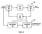
- Fig. 2 depicts a PLL 30.
- PLL 30 As part of PLL 30, or separate from PLL 30, is a detection circuit 32.
- PLL 30 comprises a phase/frequency detector 34, a low pass filter 36 and a feedback loop potentially closed by a voltage-controlled oscillator 38.
- the phase detector portion of phase/frequency detector 34 produces an output whose DC value is proportional to a phase difference between the input signal (i.e., data) and the voltage-controlled oscillator (“VCO") signal.
- VCO voltage-controlled oscillator
- the frequency detector portion detects frequency differences between those signals. Therefore, a combination of phase and frequency detection proves extremely useful since it can significantly increase the acquisition range and lock speed of the PLL.
- Low pass filter 36 suppresses high frequency components in the phase/frequency detector 34 output, allowing the DC value to control the VCO output frequency. Thus, low pass filter 36 generates the proper control voltage for VCO 3 S. The control voltage will act to change the output phase and frequency of the VCO to that of the input signal.
- the phase/frequency detector can be formulated, for example, as a multiplier (or mixer) comprising an exclusive OR gate, a R-S latch or, in the instance of frequency detection, any circuit which produces noncomplimentary outputs proportional to the frequency differences between the inputs.
- a lowpass filter can be implemented with passive elements comprising a capacitor and resistor linked between conductors bearing the input signal and the output signal.
- a VCO can be implemented, for example, as a ring oscillator comprising an odd number of series connected inverters.
- phase/frequency detector 34 need only have a phase detection component, if desired.
- the mechanism and circuitry needed to embody each component can vary depending upon the accuracy and application desired.
- the examples described above are therefore only examples of ways to implement each component. Variations and modifications may be made to the form and structure of each component as mandated by the application in which the components arc placed.
- PLL 30 may be called upon to have a frequency of the output signal be a multiple of the input signal frequency. Multiplying the input signal frequency preferably takes place in the feedback loop, whereby the output signal frequency is reduced (i.e., divided) before it is fed back to phase/frequency detector 34.
- the divisor can be modified depending on the amount of frequency multiplication needed.
- clock divider 40 includes a divisor amount N equal to or greater than 1.0. If multiplication is not needed, then N equals 1.0, Clock divider 40 is essentially a frequency divider which can be suitably configured as, for example, a digital counter.
- Detection circuit 32 is coupled to receive the input signal.
- detector circuit 32 includes a decoder 42 and a counter 44.
- Decoder 42 continuously decodes the input signal and signals the occurrence of a pattern that matches a predefined set of valid preambles.
- decoder 42 may be designed to decode a specific sequence of binary bits.
- the sequence being sought is preferably contained within a set of preambles (shown as "P" in Fig. 1) of the data stream.
- the preamble contains a coding which is sot upon transmission. If coding changes due to, for example, noise within the transmission channel or corruption as a result of connector misalignment or detachment, then the binary sequence will change.
- Decoder 42 is designed to decode a specific set of bits within the preambles. If that set does not occur for a set period of time, possibly indicated by a certain count within counter 44, then the lock/unlock signal will indicate an unlock condition.
- Counter 44 is a modulo N counter where N clock cycles is the time period between preambles. When PLL 30 is unlocked, detection of a valid preamble by the decoder resets counter 44 in the following clock cycle to synchronize it with the incoming data, If a valid preamble is detected after exactly N clock cycles, decoder 44 indicates one valid preamble has been detected. Otherwise it indicates that an invalid preamble has been detected. A preamble decoded after fewer than N clock cycles will reset counter 44 to resynchronize it again. When, for example, three valid preambles have been detected correctly, lock is declared. If PLL 30 is locked, the detection of two invalid preambles by the lock detector will cause it to declare an unlock.
- the unlock condition is commensurate with a variation in frequency of the input signal caused by noise or corruption as read by the photodetector.
- the amount of noise or corruption must be sufficient to cause a change. in the binary values of bits within the preambles. That change being unrecognizable by decoder 42, and therefore counter 44 begins counting. It is preferred that decoder 42 and counter 44 by synchronized with die output signal clocking frequency. As such, the output signal frequency clocks decoder 42 and counter 44 as shown.
- decoder 42 If decoder 42 is capable of recognizing binary bits within the preamble, then the counter will reset after a predetermined number of recognized preambles, causing the lock/unlock signal to transition back to a lock condition.
- the lock condition is commensurate with a constant phase and substantially equal frequency between the input signal and the signal forwarded via feedback - that signal being the clocking signal or a frequency divided clocking signal.
- An unlock condition indicates a variable phase and frequency difference between those signals.
- Fig. 3 illustrates a multiplexer 48 and a clock divider circuit 50.
- Output from PLL 30 is an output signal which can be fed directly to multiplexer 48, or frequency divided by circuit 50.
- the frequency divided clocking signal output from circuit 50 is then fed to multiplexer 48.
- a select input of multiplexer 48 chooses between the clocking signal output directly from PLL 30 or the frequency divided clocking signal from circuit 50. If the lock/unlock signal asserts an unlock condition, then multiplexer 48 selects the frequency divided clocking signal for input to the clock terminal of digital processor 52. If the lock/unlock signal indicates lock condition, then the clocking signal output directly from PLL 30 will be fed to the clock input of digital processor 52.
- Fig. 3 illustrates a mechanism to prevent digital processor 52 clock from exceeding its maximum operating frequency.
- the mechanism is used to divide the clocking signal sent to digital processor 52 by an appropriate factor, denoted as M in frequency divider circuit 50, whenever PLL 30 unlocks. Since PLL 30 will not lock to the corrupted data, given sufficient error coding employed within that data, digital processor 52 is protected from malfunction while PLL 30 is unlocked. If correct data resumes, PLL 30 will lock to the input signal data rate and restore the normal PLL clocking output directly to digital processor 52.
- the protection mechanism shown in Fig. 3 is beneficial when power is applied to the various components and then disturbance occurs at the cable/connector interface.
- the PLL will attempt to recover that disturbance, possibly in the form of a relatively high clock frequency.
- the PLL will receive via the photodetector a sudden increase in data rate when the connector interface is disturbed. That increase will make the PLL believe it is clocking too slow, and therefore the PLL will increase the output signal frequency to try and match the input signal frequency. In so doing, the PLL will unlock.
- the unlock condition will be immediately detected by the detection circuit looking at the incoming data stream concurrent with that data stream entering the PLL. Detection therefore occurs during PLL transients to cause immediate protection at the output of the PLL prior to entering the digital processor.
- the present system derive a clocking signal to be forwarded to the digital processor 52 from the data rate of a data stream forwarded across the transmission channel. Accordingly, the present architecture is chosen for a clock recovery function.
- PLL 30 must operate over a relatively wide frequency range to match the changing data rate.
- WO data rate within PLL 30 cannot, therefore, be crystal controlled, or fixed in any manner to a specific, limited frequency range.
- a WO which can extend its output based on a variable input frequency data stream to a range of relatively wide frequency is therefore beneficial to producing a cost-effective PLL and/or clock reference.
- the integrated circuit may include the PLL, the detection circuit, the clock divider circuit, the multiplexer, and possibly the digital processor all within a single monolithic substrate.
Landscapes
- Stabilization Of Oscillater, Synchronisation, Frequency Synthesizers (AREA)
- Synchronisation In Digital Transmission Systems (AREA)
- Networks Using Active Elements (AREA)
- Butt Welding And Welding Of Specific Article (AREA)
Abstract
Description
- This invention relates to an integrated circuit embodying a phase-locked loop ("PLL") and, more particularly, to a mechanism for controlling frequency of an output signal forwarded from the PLL whenever the PLL is unlocked.
- A PLL is generally used in many areas of electronics to control the frequency and/or phase of a signal. Instances of use include, for example, applications in frequency synthesizers, analog-digital modulators and demodulators, and clock recovery circuits.
- Clock recovery is a term generally used to describe the derivation of a clocking signal. The clocking signal is produced without having to add a timing reference to the circuit which requires the clocking signal. Clock recovery circuits therefore arise when deriving a clocking signal from data transmitted across a communication channel or network. As the stream of data flows across the channel, the clocking signal is constructed and synchronized from transitions of the data. Thus, timing information (i.e., the clocking signal) is recovered from a data stream at the receiving end of, for example, a fiberoptic transmission channel. Avoidance in having to add a separate clock transmission medium or a clock generation circuit at the receiving end circuit is paramount as to the reasons for clock recovery in general.
- The PLL compares the arrival of signal transitions on the incoming data stream with the PLL internally generated clock to increase or decrease frequency of the output signal produced from the PLL. Comparison of frequency and phase continues until The incoming data stream can be correctly decoded. Once the correct data is decoded, the PLL is said to be "locked". More specifically, a PLL is considered locked if the phase and/or frequency difference between the incoming data transitions and the PLL internally generated clock is equal or constant with time. If the PLL does not contain an internal clock divider within its feedback loop, then a locked PLL is one that implies an equal frequency and phase between the incoming data frequency (i.e., input signal frequency) and a clocking signal output from the PLL (i.e., output signal frequency). For robust operation, the PLL must be designed so that it can operate over a wide frequency lock range. A wide range is needed to ensure that the PLL can lock to the input signal data under almost all possible conditions of component variations within the PLL circuit. This wide frequency lock range can produce a wide range of clock frequencies produced at the PLL output. On the other hand, a digital processor connected to receive the PLL output clocking signal will require the output clocking signal frequency not exceed the maximum operating frequency of the processor. Therefore, the recovered clock (i.e., output signal produced by the PLL) must be one which can be controlled so that it does not exceed the maximum operating frequency of the processor if short- and long-term variations in the incoming data stream phase and/or frequency occur.
- The incoming data stream to a PLL can oftentimes be temporarily disrupted by, for example, noise placed on the transmission channel. Noise of relatively short duration can in most instances be removed by a low pass filter arranged within the PLL. It is not until, however, several sequential data bits change in phase and/or frequency that the low pass filter can no longer discern and therefore filter that variation.
One example of a relatively long-term variation is shown in reference to Fig. 1. In particular, anoptical connector 10 is shown connected to one end of afiberoptic cable 12.Cable 12 comprises acylindrical core 14 arranged in contact with the inner surface of acladding material 16.Core 14 is made of a transparent dielectric material having a refractive index preferably greater than cladding 16. -
Connector 10 includes amechanical attachment mechanism 18 for securing it tocable 12,Connector 10 houses at least onephotodetector 20. Photodetector 20 includes any device capable of accepting light energy and converting into an electrical signal. Popular photodetectors include solid state devices, such as silicon photodiodes, phototransistors, and photo-Darlingtons. To ensure accurate reproduction, coupling betweenconnector 10 andcable 12 must be carefully and precisely made, Special connectors have been designed to mechanically mate and align the transmission path ofcable 12 to itsrespective photodetector 20. Those connectors afford multiple connect and disconnect while maintaining proper alignment in the interim. Unfortunately, eachtime connector 10 is displaced fromcable 12, the phase read byphotodetector 20 of any data forwarded throughcable 12 changes. Thus, only minor change in the spatial relationship betweenphotodetector 20 and the distal end ofcable 12 modify the phase and/or frequency recorded byphotodetector 20. If the distance betweenphotodetector 20 andcable 12 is altered (e.g., by disconnect or connect) whiledata stream 22 is being transmitted, the integrity ofdata stream 22 may be corrupted. Incorrectly formed transitions ofdata stream 22 which last for a sufficiently long time are, unfortunately, recorded by the PLL which then attempts to recover a clocking signal based on those transitions. - A relatively long duration of corrupted data cannot be removed by the low pass filter, and will instead cause the PLL clocking signal frequency to rapidly rise or fall. The clocking signal output from the PLL is, unfortunately, forwarded to digital circuits at the receive end of the fiberoptic cable. For example, the digital circuits may include a digital processor which is intended to operate within a pre-defined operating frequency. If the PLL clocking signal (forwarded as an output signal from the PLL) as presented to the digital processor clock input exceeds the maximum frequency of that processor, then the processor will malfunction.
- US-A-5,406,590 discloses an integrated circuit comprising: a phase-locked loop (PLL) to receive an input signal and, in response to the input signal, to produce an output signal. The PLL includes a detection circuit for dispatching a signal indicating a lock/unlock condition, and a clock divider coupled to the output signal to produce a frequency divided clocking signal. Tristate output buffers disable all output signals when an unlock condition exists, in order to avoid a malfunction of the processor due to an input exceeding the maximum frequency of that processor. Disabling the output signal of the PLL, however, causes any clocked components of the digital processor to become inactive. During instances in which the PLL is unlocked, the digital circuit and/or processor does therefore not operate.
US 5,579,353 discloses a dynamic clock mode switch which delivers a PLL clock to a depending system when the PLL is locked. In an unlocked state the PLL is bypassed and the reference clock is delivered to the depending system. - The problems outlined above are in large part solved by an improved apparatus, preferably formed as an integrated circuit containing a PLL. In particular, an improved circuit is presented in which the clocking signal frequency output from the PLL is controlled during times when the PLL is unlocked. During instances in which the PLL is unlocked, the clocking signal is regulated to a lower frequency than what would normally be produced from the PLL. That regulated frequency is one chosen to be within the operating frequency of the digital circuit and/or processor.
- According to one embodiment, a detection circuit is used to determine when the data stream is corrupted. Sufficient corruption for a sufficient amount of time is decoded as an unlock signal. The unlock signal serves to select a frequency divided clocking signal output from a clock divider circuit, The clock divider circuit is coupled between the output from the PLL and a multiplexer, whose input is selectable by the current state of the unlock signal. The multiplexer is coupled to receive a frequency divided clocking signal output from the clock divider and the clocking signal output from the PLL. During times when the unlock signal is asserted, the multiplexer selects the frequency divided clocking signal; during times when the unlock signal is not present, the multiplexer selects the clocking signal output from the PLL. Accordingly, the frequency divided clocking signal is derived from and of lesser frequency than the clocking signal. Selectable output from the multiplexer is connected to the clocking input of the digital circuit/processor.
- Broadly speaking, the present invention contemplates a PLL. The PLL comprises a detection circuit adapted for receiving an input signal forwarded to the PLL. The detection circuit is further adapted for dispatching an unlock signal indicating a change in frequency of the input signal. The change in frequency may be brought about by movement of the coupling relative the fiberoptic cable. The change in frequency can be of long duration dictated by the time it takes to disconnect and/or reconnect the connector to the cable. A multiplexer is further included to receive the unlock signal. Responsive to the unlock signal the multiplexer can select as input to a digital process a frequency divided clocking signal rather than the normal PLL clocking signal.
- The present invention further contemplates an integrated circuit for selectively controlling the operating frequency of a digital processor. According to one embodiment, the integrated circuit includes a PLL, a clock divider circuit and a multiplexer. According to another embodiment, the clock divider circuit and the multiplexer form a part of the PLL. The PLL produces an output signal in response to an input signal. If the PLL is locked and clock division/multiplication within the PLL does not occur, the input and output signal frequencies are substantially equal. If the frequency of the input signal exceeds a predefined amount, an unlock condition may occur momentarily. A detection circuit senses the unlock condition and dispatches an unlock signal to the multiplexer. The unlock signal selects either the output signal (i.e., clocking signal) forwarded from the PLL or a frequency divided clocking signal forwarded from the clock divider circuit. On receiving an unlock signal, the multiplexer selects the frequency divided clocking signal; on receiving a lock signal, the multiplexer selects the output signal. The selected signal and, more particularly, the frequency of the selected signal is forwarded to the clocking input of the digital processor to ensure the digital processor does not operate outside its specified frequency range.
- Other objects and advantages of the invention will become apparent upon reading the following detailed description and upon reference to the accompanying drawings in which:
- Fig. 1
- is a partial cross-sectional view of a fiberoptic cable having a data stream forwarded to one end of the cable and a connector containing a photodetector coupled to the other end of the cable;
- Fig. 2
- is a block diagram of a PLL and a detection circuit coupled to receive an input signal and produce a clocking signal and a lock/unlock signal, respectively; and
- Fig. 3
- is a block diagram of a multiplexer coupled to forward to a digital processor clock input either the clocking signal or a frequency divided clocking signal produced from a clock divider circuit, based on the status of the lock/unlock signal.
- Turning now the drawings, Fig. 2 depicts a
PLL 30. As part ofPLL 30, or separate fromPLL 30, is adetection circuit 32. In its simplest form,PLL 30 comprises a phase/frequency detector 34, alow pass filter 36 and a feedback loop potentially closed by a voltage-controlledoscillator 38. The phase detector portion of phase/frequency detector 34 produces an output whose DC value is proportional to a phase difference between the input signal (i.e., data) and the voltage-controlled oscillator ("VCO") signal. The frequency detector portion detects frequency differences between those signals. Therefore, a combination of phase and frequency detection proves extremely useful since it can significantly increase the acquisition range and lock speed of the PLL.Low pass filter 36 suppresses high frequency components in the phase/frequency detector 34 output, allowing the DC value to control the VCO output frequency. Thus,low pass filter 36 generates the proper control voltage for VCO 3 S. The control voltage will act to change the output phase and frequency of the VCO to that of the input signal. - The phase/frequency detector can be formulated, for example, as a multiplier (or mixer) comprising an exclusive OR gate, a R-S latch or, in the instance of frequency detection, any circuit which produces noncomplimentary outputs proportional to the frequency differences between the inputs. In its simplest form, a lowpass filter can be implemented with passive elements comprising a capacitor and resistor linked between conductors bearing the input signal and the output signal. A VCO can be implemented, for example, as a ring oscillator comprising an odd number of series connected inverters.
- The components shown in
PLL 30 can be made in numerous different ways. For example, phase/frequency detector 34 need only have a phase detection component, if desired. Thus, the mechanism and circuitry needed to embody each component can vary depending upon the accuracy and application desired. The examples described above are therefore only examples of ways to implement each component. Variations and modifications may be made to the form and structure of each component as mandated by the application in which the components arc placed. -
PLL 30 may be called upon to have a frequency of the output signal be a multiple of the input signal frequency. Multiplying the input signal frequency preferably takes place in the feedback loop, whereby the output signal frequency is reduced (i.e., divided) before it is fed back to phase/frequency detector 34. The divisor can be modified depending on the amount of frequency multiplication needed. Thus, clock divider 40 includes a divisor amount N equal to or greater than 1.0. If multiplication is not needed, then N equals 1.0, Clock divider 40 is essentially a frequency divider which can be suitably configured as, for example, a digital counter. -
Detection circuit 32 is coupled to receive the input signal. According to one embodiment,detector circuit 32 includes adecoder 42 and acounter 44.Decoder 42 continuously decodes the input signal and signals the occurrence of a pattern that matches a predefined set of valid preambles. Thus,decoder 42 may be designed to decode a specific sequence of binary bits. The sequence being sought is preferably contained within a set of preambles (shown as "P" in Fig. 1) of the data stream. The preamble contains a coding which is sot upon transmission. If coding changes due to, for example, noise within the transmission channel or corruption as a result of connector misalignment or detachment, then the binary sequence will change.Decoder 42 is designed to decode a specific set of bits within the preambles. If that set does not occur for a set period of time, possibly indicated by a certain count withincounter 44, then the lock/unlock signal will indicate an unlock condition.Counter 44 is a modulo N counter where N clock cycles is the time period between preambles. WhenPLL 30 is unlocked, detection of a valid preamble by the decoder resets counter 44 in the following clock cycle to synchronize it with the incoming data, If a valid preamble is detected after exactly N clock cycles,decoder 44 indicates one valid preamble has been detected. Otherwise it indicates that an invalid preamble has been detected. A preamble decoded after fewer than N clock cycles will reset counter 44 to resynchronize it again. When, for example, three valid preambles have been detected correctly, lock is declared. IfPLL 30 is locked, the detection of two invalid preambles by the lock detector will cause it to declare an unlock. - The unlock condition is commensurate with a variation in frequency of the input signal caused by noise or corruption as read by the photodetector. The amount of noise or corruption must be sufficient to cause a change. in the binary values of bits within the preambles. That change being unrecognizable by
decoder 42, and therefore counter 44 begins counting. It is preferred thatdecoder 42 and counter 44 by synchronized with die output signal clocking frequency. As such, the output signalfrequency clocks decoder 42 and counter 44 as shown. - If
decoder 42 is capable of recognizing binary bits within the preamble, then the counter will reset after a predetermined number of recognized preambles, causing the lock/unlock signal to transition back to a lock condition. The lock condition is commensurate with a constant phase and substantially equal frequency between the input signal and the signal forwarded via feedback - that signal being the clocking signal or a frequency divided clocking signal. An unlock condition indicates a variable phase and frequency difference between those signals. - Fig. 3 illustrates a
multiplexer 48 and aclock divider circuit 50. Output fromPLL 30 is an output signal which can be fed directly tomultiplexer 48, or frequency divided bycircuit 50. The frequency divided clocking signal output fromcircuit 50 is then fed tomultiplexer 48. A select input ofmultiplexer 48 chooses between the clocking signal output directly fromPLL 30 or the frequency divided clocking signal fromcircuit 50. If the lock/unlock signal asserts an unlock condition, then multiplexer 48 selects the frequency divided clocking signal for input to the clock terminal ofdigital processor 52. If the lock/unlock signal indicates lock condition, then the clocking signal output directly fromPLL 30 will be fed to the clock input ofdigital processor 52. - Fig. 3 illustrates a mechanism to prevent
digital processor 52 clock from exceeding its maximum operating frequency. The mechanism is used to divide the clocking signal sent todigital processor 52 by an appropriate factor, denoted as M infrequency divider circuit 50, wheneverPLL 30 unlocks. SincePLL 30 will not lock to the corrupted data, given sufficient error coding employed within that data,digital processor 52 is protected from malfunction whilePLL 30 is unlocked. If correct data resumes,PLL 30 will lock to the input signal data rate and restore the normal PLL clocking output directly todigital processor 52. - The protection mechanism shown in Fig. 3 is beneficial when power is applied to the various components and then disturbance occurs at the cable/connector interface. The PLL will attempt to recover that disturbance, possibly in the form of a relatively high clock frequency. Specifically, the PLL will receive via the photodetector a sudden increase in data rate when the connector interface is disturbed. That increase will make the PLL believe it is clocking too slow, and therefore the PLL will increase the output signal frequency to try and match the input signal frequency. In so doing, the PLL will unlock. The unlock condition will be immediately detected by the detection circuit looking at the incoming data stream concurrent with that data stream entering the PLL. Detection therefore occurs during PLL transients to cause immediate protection at the output of the PLL prior to entering the digital processor. Decoding an unlock condition concurrent with that condition's effect on the PLL affords immediate responsiveness, and regulation, prior to transferring the unlocked (unregulated high frequency) to the digital processor. Intervention is achieved in a relatively simplistic fashion using a clock divider and a multiplexer to scale down the clocking signal seen by the digital processor as soon as an unlock state occurs. Reducing the clocking signal to a portion of what would be a relatively high clocking output from an unlocked PLL prevents the digital processor from operating outside its maximum operating frequency. The amount of clock division within
circuit 50 can be varied depending on the potential high frequency output from PLL, and the acceptable operating frequency ofdigital processor 52. - It is intended that the present system derive a clocking signal to be forwarded to the
digital processor 52 from the data rate of a data stream forwarded across the transmission channel. Accordingly, the present architecture is chosen for a clock recovery function. - It is recognized that the data rate can change significantly, depending on the transmitter, receiver and transmission media. For this reason,
PLL 30 must operate over a relatively wide frequency range to match the changing data rate. WO data rate withinPLL 30 cannot, therefore, be crystal controlled, or fixed in any manner to a specific, limited frequency range. A WO which can extend its output based on a variable input frequency data stream to a range of relatively wide frequency is therefore beneficial to producing a cost-effective PLL and/or clock reference. - It will be appreciated by those skilled in the art having the benefit of this disclosure, that this invention is believed to be capable of applications with any integrated circuit having both analog and digital portions. The integrated circuit may include the PLL, the detection circuit, the clock divider circuit, the multiplexer, and possibly the digital processor all within a single monolithic substrate.
Claims (12)
- An apparatus comprising a phase-locked loop (30) which is configured to receive an input data stream (DATA) and to generate a clocking signal, and
a detection circuit (32) for dispatching an unlock signal (LOCK/UNLOCK),
characterized in
the detection circuit being configured to signaling an unlock state when an input data stream to the phase-locked loop does not match a predefined set of valid preambles, and
a circuit being provided for regulating the clocking signal, which upon receiving the unlock signal, regulates the clocking signal to a lower frequency than what would normally be produced from the phase-locked loop. - An apparatus as claimed in claim 1, wherein the means for regulating the clocking signal comprises a multiplexer (48) which normally selects the clocking signal generated by the phase-locked loop and in case of an unlock signal selects a frequency divided clocking signal generated by a frequency divider from the phase-locked loop.
- An apparatus as claimed in claim 1, wherein the detection circuit (32) comprises a decoder (42).
- An apparatus as claimed in claim 3, wherein the detection circuit (32) comprises a decoder (42) and a counter (44) serially coupled to one another for dispatching the unlock signal when the input signal comprises at least two successive sets of erroneous binary code.
- An apparatus as claimed in claim 1, wherein a frequency divided clocking signal is output from a clock divider circuit (50) coupled to receive an output signal from the phase-looked loop (30).
- An apparatus as claimed in claim 5, wherein the clock divider circuit (50) is coupled to divide a frequency of the output signal forwarded from the phase-locked loop (30).
- An apparatus as claimed in claim 6, wherein the frequency of the output signal is at least equal to the frequency of the input signal.
- An apparatus as claimed in claim 1, further comprising a digital processor (52) coupled to receive the frequency divided clocking signal.
- An apparatus as claimed in claim 1, comprising an integrated circuit for selectively controlling the operating frequency of a digital processor (52), including:a phase-locked loop coupled to receive an input signal (DATA) and, in response to the input signal, to produce an output signal (CLK),a detection circuit (32) coupled to dispatch an unlock signal (LOCK/UNLOCK) if an input data stream to the phase-locked loop does not match a predefined set of valid preambles,a clock divider circuit (50) coupled to receive the output signal and divide the frequency of the output signal to produce a frequency divided clocking signal; anda multiplexer (48) coupled to forward the frequency divided clocking signal to the digital processor (52) upon receiving the unlock signal.
- An apparatus as claimed in claim 9, wherein the frequency divided clocking signal transitions at a frequency which is a division of the frequency of the output clocking signal.
- An apparatus as claimed in claim 9, wherein the multiplexer (48) is coupled to receive the frequency divided clocking signal, the output clocking signal and the unlock signal.
- An apparatus as claimed in claim 9, wherein the frequency divided clocking signal is strobed at a frequency within the operating frequency of the digital processor (52).
Applications Claiming Priority (3)
| Application Number | Priority Date | Filing Date | Title |
|---|---|---|---|
| US951796 | 1997-10-16 | ||
| US08/951,796 US6005904A (en) | 1997-10-16 | 1997-10-16 | Phase-locked loop with protected output during instances when the phase-locked loop is unlocked |
| EP98951043A EP1012979B1 (en) | 1997-10-16 | 1998-10-13 | Phase-locked loop and integrated circuit therefor |
Related Parent Applications (1)
| Application Number | Title | Priority Date | Filing Date |
|---|---|---|---|
| EP98951043A Division EP1012979B1 (en) | 1997-10-16 | 1998-10-13 | Phase-locked loop and integrated circuit therefor |
Publications (2)
| Publication Number | Publication Date |
|---|---|
| EP1333580A1 EP1333580A1 (en) | 2003-08-06 |
| EP1333580B1 true EP1333580B1 (en) | 2006-04-26 |
Family
ID=25492161
Family Applications (2)
| Application Number | Title | Priority Date | Filing Date |
|---|---|---|---|
| EP98951043A Expired - Lifetime EP1012979B1 (en) | 1997-10-16 | 1998-10-13 | Phase-locked loop and integrated circuit therefor |
| EP03007754A Expired - Lifetime EP1333580B1 (en) | 1997-10-16 | 1998-10-13 | Apparatus comprising a phase-locked loop |
Family Applications Before (1)
| Application Number | Title | Priority Date | Filing Date |
|---|---|---|---|
| EP98951043A Expired - Lifetime EP1012979B1 (en) | 1997-10-16 | 1998-10-13 | Phase-locked loop and integrated circuit therefor |
Country Status (7)
| Country | Link |
|---|---|
| US (1) | US6005904A (en) |
| EP (2) | EP1012979B1 (en) |
| JP (1) | JP4034515B2 (en) |
| AT (2) | ATE246415T1 (en) |
| AU (1) | AU9693698A (en) |
| DE (2) | DE69816838T9 (en) |
| WO (1) | WO1999021280A1 (en) |
Families Citing this family (73)
| Publication number | Priority date | Publication date | Assignee | Title |
|---|---|---|---|---|
| US6292522B1 (en) * | 1997-11-13 | 2001-09-18 | Lsi Logic Corporation | Frequency decoder databank for phase-locked loop |
| JP4015254B2 (en) * | 1998-01-16 | 2007-11-28 | 富士通株式会社 | Lock detection circuit and PLL frequency synthesizer |
| US6163583A (en) * | 1998-03-25 | 2000-12-19 | Sony Corporation Of Japan | Dynamic clocking apparatus and system for reducing power dissipation |
| JPH11353878A (en) * | 1998-04-07 | 1999-12-24 | Fujitsu Ltd | Semiconductor device |
| EP0966103B1 (en) * | 1998-06-17 | 2006-04-19 | STMicroelectronics N.V. | Frequency synthesiser |
| US6763060B1 (en) * | 1999-02-19 | 2004-07-13 | Oasis Silicon Systems | Communication system employing a network of power managed transceivers that can generate a clocking signal or enable data bypass of a digital system associated with each transceiver |
| US6853696B1 (en) * | 1999-12-20 | 2005-02-08 | Nortel Networks Limited | Method and apparatus for clock recovery and data qualification |
| KR100318431B1 (en) * | 1999-12-24 | 2001-12-24 | 박종섭 | A very compact Delay Locked Loop using bi-directional ring oscillator and counter |
| US6708026B1 (en) * | 2000-01-11 | 2004-03-16 | Ericsson Inc. | Division based local oscillator for frequency synthesis |
| US6633186B1 (en) * | 2000-04-17 | 2003-10-14 | Intel Corporation | Speed-locked loop to provide speed information based on die operating conditions |
| US6782068B1 (en) * | 2000-06-30 | 2004-08-24 | Cypress Semiconductor Corp. | PLL lockout watchdog |
| US6294935B1 (en) * | 2000-10-17 | 2001-09-25 | Vlsi Technology, Inc. | Built-in-self-test circuitry for testing a phase locked loop circuit |
| US8176296B2 (en) | 2000-10-26 | 2012-05-08 | Cypress Semiconductor Corporation | Programmable microcontroller architecture |
| US8103496B1 (en) | 2000-10-26 | 2012-01-24 | Cypress Semicondutor Corporation | Breakpoint control in an in-circuit emulation system |
| US8149048B1 (en) | 2000-10-26 | 2012-04-03 | Cypress Semiconductor Corporation | Apparatus and method for programmable power management in a programmable analog circuit block |
| US8160864B1 (en) | 2000-10-26 | 2012-04-17 | Cypress Semiconductor Corporation | In-circuit emulator and pod synchronized boot |
| US6724220B1 (en) | 2000-10-26 | 2004-04-20 | Cyress Semiconductor Corporation | Programmable microcontroller architecture (mixed analog/digital) |
| US7765095B1 (en) | 2000-10-26 | 2010-07-27 | Cypress Semiconductor Corporation | Conditional branching in an in-circuit emulation system |
| US8385476B2 (en) | 2001-04-25 | 2013-02-26 | Texas Instruments Incorporated | Digital phase locked loop |
| US6873195B2 (en) * | 2001-08-22 | 2005-03-29 | Bigband Networks Bas, Inc. | Compensating for differences between clock signals |
| WO2003021439A1 (en) | 2001-08-29 | 2003-03-13 | Analog Devices, Inc. | Methods and apparatus for improving throughput of cache-based embedded processors by switching tasks in response to a cache miss |
| US6744323B1 (en) * | 2001-08-30 | 2004-06-01 | Cypress Semiconductor Corp. | Method for phase locking in a phase lock loop |
| US7406674B1 (en) | 2001-10-24 | 2008-07-29 | Cypress Semiconductor Corporation | Method and apparatus for generating microcontroller configuration information |
| US8078970B1 (en) | 2001-11-09 | 2011-12-13 | Cypress Semiconductor Corporation | Graphical user interface with user-selectable list-box |
| US8042093B1 (en) | 2001-11-15 | 2011-10-18 | Cypress Semiconductor Corporation | System providing automatic source code generation for personalization and parameterization of user modules |
| US7770113B1 (en) | 2001-11-19 | 2010-08-03 | Cypress Semiconductor Corporation | System and method for dynamically generating a configuration datasheet |
| US6971004B1 (en) | 2001-11-19 | 2005-11-29 | Cypress Semiconductor Corp. | System and method of dynamically reconfiguring a programmable integrated circuit |
| US7774190B1 (en) | 2001-11-19 | 2010-08-10 | Cypress Semiconductor Corporation | Sleep and stall in an in-circuit emulation system |
| US7844437B1 (en) | 2001-11-19 | 2010-11-30 | Cypress Semiconductor Corporation | System and method for performing next placements and pruning of disallowed placements for programming an integrated circuit |
| US8069405B1 (en) | 2001-11-19 | 2011-11-29 | Cypress Semiconductor Corporation | User interface for efficiently browsing an electronic document using data-driven tabs |
| US20030115503A1 (en) * | 2001-12-14 | 2003-06-19 | Koninklijke Philips Electronics N.V. | System for enhancing fault tolerance and security of a computing system |
| US8103497B1 (en) | 2002-03-28 | 2012-01-24 | Cypress Semiconductor Corporation | External interface for event architecture |
| US7308608B1 (en) | 2002-05-01 | 2007-12-11 | Cypress Semiconductor Corporation | Reconfigurable testing system and method |
| JP4370246B2 (en) * | 2002-06-21 | 2009-11-25 | トムソン ライセンシング | Clock extraction circuit for linearly expandable broadcast router |
| US7761845B1 (en) | 2002-09-09 | 2010-07-20 | Cypress Semiconductor Corporation | Method for parameterizing a user module |
| US7882369B1 (en) * | 2002-11-14 | 2011-02-01 | Nvidia Corporation | Processor performance adjustment system and method |
| US7636411B2 (en) * | 2003-06-30 | 2009-12-22 | Intel Corporation | I/O link with configurable forwarded and derived clocks |
| DE10330593B4 (en) * | 2003-07-07 | 2010-11-04 | Qimonda Ag | Integrated clock supply module for a memory module, memory module, which includes the integrated clock supply module, as well as methods for operating the memory module under test conditions |
| CN100565422C (en) * | 2004-01-29 | 2009-12-02 | Nxp股份有限公司 | Programmable and abortable clock generation unit |
| US7295049B1 (en) | 2004-03-25 | 2007-11-13 | Cypress Semiconductor Corporation | Method and circuit for rapid alignment of signals |
| US8286125B2 (en) | 2004-08-13 | 2012-10-09 | Cypress Semiconductor Corporation | Model for a hardware device-independent method of defining embedded firmware for programmable systems |
| US8069436B2 (en) | 2004-08-13 | 2011-11-29 | Cypress Semiconductor Corporation | Providing hardware independence to automate code generation of processing device firmware |
| US7332976B1 (en) | 2005-02-04 | 2008-02-19 | Cypress Semiconductor Corporation | Poly-phase frequency synthesis oscillator |
| US7400183B1 (en) | 2005-05-05 | 2008-07-15 | Cypress Semiconductor Corporation | Voltage controlled oscillator delay cell and method |
| US8089461B2 (en) | 2005-06-23 | 2012-01-03 | Cypress Semiconductor Corporation | Touch wake for electronic devices |
| US8085067B1 (en) | 2005-12-21 | 2011-12-27 | Cypress Semiconductor Corporation | Differential-to-single ended signal converter circuit and method |
| US8067948B2 (en) | 2006-03-27 | 2011-11-29 | Cypress Semiconductor Corporation | Input/output multiplexer bus |
| JP4745127B2 (en) * | 2006-05-23 | 2011-08-10 | ルネサスエレクトロニクス株式会社 | Clock switching circuit |
| US8026739B2 (en) | 2007-04-17 | 2011-09-27 | Cypress Semiconductor Corporation | System level interconnect with programmable switching |
| US8130025B2 (en) | 2007-04-17 | 2012-03-06 | Cypress Semiconductor Corporation | Numerical band gap |
| US7737724B2 (en) | 2007-04-17 | 2010-06-15 | Cypress Semiconductor Corporation | Universal digital block interconnection and channel routing |
| US9564902B2 (en) | 2007-04-17 | 2017-02-07 | Cypress Semiconductor Corporation | Dynamically configurable and re-configurable data path |
| US8516025B2 (en) | 2007-04-17 | 2013-08-20 | Cypress Semiconductor Corporation | Clock driven dynamic datapath chaining |
| US8040266B2 (en) | 2007-04-17 | 2011-10-18 | Cypress Semiconductor Corporation | Programmable sigma-delta analog-to-digital converter |
| US8092083B2 (en) | 2007-04-17 | 2012-01-10 | Cypress Semiconductor Corporation | Temperature sensor with digital bandgap |
| US8266575B1 (en) | 2007-04-25 | 2012-09-11 | Cypress Semiconductor Corporation | Systems and methods for dynamically reconfiguring a programmable system on a chip |
| US9720805B1 (en) | 2007-04-25 | 2017-08-01 | Cypress Semiconductor Corporation | System and method for controlling a target device |
| US8065653B1 (en) | 2007-04-25 | 2011-11-22 | Cypress Semiconductor Corporation | Configuration of programmable IC design elements |
| US9134782B2 (en) | 2007-05-07 | 2015-09-15 | Nvidia Corporation | Maintaining optimum voltage supply to match performance of an integrated circuit |
| US8049569B1 (en) | 2007-09-05 | 2011-11-01 | Cypress Semiconductor Corporation | Circuit and method for improving the accuracy of a crystal-less oscillator having dual-frequency modes |
| US8370663B2 (en) | 2008-02-11 | 2013-02-05 | Nvidia Corporation | Power management with dynamic frequency adjustments |
| RU2399155C1 (en) * | 2009-03-23 | 2010-09-10 | Открытое Акционерное Общество "Российские Железные Дороги" | Method for lock synchronisation of generators of railway digital communication network |
| US9448964B2 (en) | 2009-05-04 | 2016-09-20 | Cypress Semiconductor Corporation | Autonomous control in a programmable system |
| US9256265B2 (en) | 2009-12-30 | 2016-02-09 | Nvidia Corporation | Method and system for artificially and dynamically limiting the framerate of a graphics processing unit |
| US9830889B2 (en) | 2009-12-31 | 2017-11-28 | Nvidia Corporation | Methods and system for artifically and dynamically limiting the display resolution of an application |
| US8839006B2 (en) | 2010-05-28 | 2014-09-16 | Nvidia Corporation | Power consumption reduction systems and methods |
| US20120166859A1 (en) * | 2010-12-22 | 2012-06-28 | Fernald Kenneth W | Method and apparatus for generating a system clock signal |
| US8730402B2 (en) * | 2011-04-21 | 2014-05-20 | Samsung Electronics Co., Ltd. | Analog front end for DTV, DTV system having the same, and operation methods thereof |
| JP2014090344A (en) | 2012-10-31 | 2014-05-15 | Nec Corp | Clock signal initialization circuit and method |
| WO2015135490A1 (en) * | 2014-03-12 | 2015-09-17 | Mediatek Singapore Pte. Ltd. | Divisor control circuit, fractional frequency division device, frequency synthesizer and frequency synthesis method |
| US10389366B2 (en) * | 2017-06-29 | 2019-08-20 | Qualcomm Incorporated | SerDes with adaptive clock data recovery |
| US10698439B1 (en) * | 2019-01-31 | 2020-06-30 | Qualcomm Incorporated | Efficient clock forwarding scheme |
| US12088303B1 (en) | 2023-02-23 | 2024-09-10 | Qualcomm Incorporated | Self-calibrated phase tuning system |
Family Cites Families (13)
| Publication number | Priority date | Publication date | Assignee | Title |
|---|---|---|---|---|
| US4534044A (en) * | 1983-05-02 | 1985-08-06 | Honeywell Information Systems Inc. | Diskette read data recovery system |
| US4849998A (en) * | 1988-06-03 | 1989-07-18 | Communications Satellite Corporation | Rate synchronized symbol timing recovery for variable rate data transmission systems |
| JP2664249B2 (en) * | 1989-03-13 | 1997-10-15 | 株式会社日立製作所 | Timing extraction circuit, communication system using the same, timing extraction method, and communication device |
| US5184350A (en) * | 1991-04-17 | 1993-02-02 | Raytheon Company | Telephone communication system having an enhanced timing circuit |
| US5406590A (en) * | 1992-10-23 | 1995-04-11 | Compaq Computer Corporation | Method of and apparatus for correcting edge placement errors in multiplying phase locked loop circuits |
| JPH06268518A (en) * | 1993-03-09 | 1994-09-22 | Sony Corp | Variable oscillator circuit |
| US5579353A (en) * | 1993-10-12 | 1996-11-26 | Texas Instruments Incorporated | Dynamic clock mode switch |
| JPH07307064A (en) * | 1994-05-11 | 1995-11-21 | Canon Inc | Optical information reproducing device |
| JP2755183B2 (en) * | 1994-09-26 | 1998-05-20 | 日本電気株式会社 | LSI with built-in clock generator / controller for low power consumption operation |
| US5838749A (en) * | 1995-06-05 | 1998-11-17 | Broadband Communications Products, Inc. | Method and apparatus for extracting an embedded clock from a digital data signal |
| JPH0983356A (en) * | 1995-09-08 | 1997-03-28 | Kawasaki Steel Corp | Clock generator |
| JPH0993126A (en) * | 1995-09-28 | 1997-04-04 | Nec Corp | Clock generator |
| US5963068A (en) * | 1997-07-28 | 1999-10-05 | Motorola Inc. | Fast start-up processor clock generation method and system |
-
1997
- 1997-10-16 US US08/951,796 patent/US6005904A/en not_active Expired - Lifetime
-
1998
- 1998-10-13 EP EP98951043A patent/EP1012979B1/en not_active Expired - Lifetime
- 1998-10-13 AT AT98951043T patent/ATE246415T1/en not_active IP Right Cessation
- 1998-10-13 DE DE69816838T patent/DE69816838T9/en active Active
- 1998-10-13 AT AT03007754T patent/ATE324707T1/en not_active IP Right Cessation
- 1998-10-13 WO PCT/US1998/021512 patent/WO1999021280A1/en not_active Ceased
- 1998-10-13 AU AU96936/98A patent/AU9693698A/en not_active Abandoned
- 1998-10-13 JP JP2000517487A patent/JP4034515B2/en not_active Expired - Lifetime
- 1998-10-13 DE DE69834354T patent/DE69834354T2/en not_active Expired - Lifetime
- 1998-10-13 EP EP03007754A patent/EP1333580B1/en not_active Expired - Lifetime
Also Published As
| Publication number | Publication date |
|---|---|
| JP4034515B2 (en) | 2008-01-16 |
| EP1012979A1 (en) | 2000-06-28 |
| ATE324707T1 (en) | 2006-05-15 |
| DE69816838T9 (en) | 2005-02-17 |
| ATE246415T1 (en) | 2003-08-15 |
| WO1999021280A1 (en) | 1999-04-29 |
| EP1012979B1 (en) | 2003-07-30 |
| EP1333580A1 (en) | 2003-08-06 |
| DE69834354D1 (en) | 2006-06-01 |
| JP2001521316A (en) | 2001-11-06 |
| US6005904A (en) | 1999-12-21 |
| DE69834354T2 (en) | 2006-08-31 |
| AU9693698A (en) | 1999-05-10 |
| DE69816838T2 (en) | 2004-04-22 |
| DE69816838D1 (en) | 2003-09-04 |
Similar Documents
| Publication | Publication Date | Title |
|---|---|---|
| EP1012979B1 (en) | Phase-locked loop and integrated circuit therefor | |
| US5194828A (en) | Double PLL device | |
| US4972442A (en) | Phase-locked loop clock | |
| US7203260B2 (en) | Tracked 3X oversampling receiver | |
| KR910003027B1 (en) | Digital phase synchronizing loop | |
| US4167760A (en) | Bi-phase decoder apparatus and method | |
| EP0755135A2 (en) | Apparatus and method for recovering a clock signal | |
| US5406590A (en) | Method of and apparatus for correcting edge placement errors in multiplying phase locked loop circuits | |
| JPH0824261B2 (en) | PLL monitoring circuit | |
| US6236697B1 (en) | Clock recovery for multiple frequency input data | |
| WO1999022482A1 (en) | Clock recovery circuit | |
| US20060023824A1 (en) | Method and device for extracting a clock frequency underlying a data stream | |
| WO1994008285A1 (en) | Method of and apparatus for startup of a digital computer system clock | |
| US5751775A (en) | Transmission circuit of a line encoded signal on a telephone line | |
| US5666388A (en) | Clock recovery circuit with matched oscillators | |
| JPH07506470A (en) | Method and apparatus for providing digital audio interface protocol | |
| CA2064320C (en) | Clock recovery circuit with memory storage level comparison with high, medium and low thresholds | |
| EP0880824B1 (en) | Phase noise reduction circuits | |
| US5003308A (en) | Serial data receiver with phase shift detection | |
| US6339833B1 (en) | Automatic recovery from clock signal loss | |
| US7081583B2 (en) | Digitally controllable oscillator | |
| US4141046A (en) | Floppy disc data separator for use with single density encoding | |
| US6400614B1 (en) | Transmission device and integrated circuit | |
| JPS62105077A (en) | Time device | |
| JP3181814B2 (en) | Phase locked loop |
Legal Events
| Date | Code | Title | Description |
|---|---|---|---|
| PUAI | Public reference made under article 153(3) epc to a published international application that has entered the european phase |
Free format text: ORIGINAL CODE: 0009012 |
|
| AC | Divisional application: reference to earlier application |
Ref document number: 1012979 Country of ref document: EP Kind code of ref document: P |
|
| AK | Designated contracting states |
Designated state(s): AT DE FI FR GB IT NL SE |
|
| 17P | Request for examination filed |
Effective date: 20040206 |
|
| AKX | Designation fees paid |
Designated state(s): AT DE FI FR GB IT NL SE |
|
| 17Q | First examination report despatched |
Effective date: 20041104 |
|
| GRAP | Despatch of communication of intention to grant a patent |
Free format text: ORIGINAL CODE: EPIDOSNIGR1 |
|
| GRAS | Grant fee paid |
Free format text: ORIGINAL CODE: EPIDOSNIGR3 |
|
| GRAA | (expected) grant |
Free format text: ORIGINAL CODE: 0009210 |
|
| AC | Divisional application: reference to earlier application |
Ref document number: 1012979 Country of ref document: EP Kind code of ref document: P |
|
| AK | Designated contracting states |
Kind code of ref document: B1 Designated state(s): AT DE FI FR GB IT NL SE |
|
| PG25 | Lapsed in a contracting state [announced via postgrant information from national office to epo] |
Ref country code: IT Free format text: LAPSE BECAUSE OF FAILURE TO SUBMIT A TRANSLATION OF THE DESCRIPTION OR TO PAY THE FEE WITHIN THE PRESCRIBED TIME-LIMIT;WARNING: LAPSES OF ITALIAN PATENTS WITH EFFECTIVE DATE BEFORE 2007 MAY HAVE OCCURRED AT ANY TIME BEFORE 2007. THE CORRECT EFFECTIVE DATE MAY BE DIFFERENT FROM THE ONE RECORDED. Effective date: 20060426 Ref country code: AT Free format text: LAPSE BECAUSE OF FAILURE TO SUBMIT A TRANSLATION OF THE DESCRIPTION OR TO PAY THE FEE WITHIN THE PRESCRIBED TIME-LIMIT Effective date: 20060426 Ref country code: FI Free format text: LAPSE BECAUSE OF FAILURE TO SUBMIT A TRANSLATION OF THE DESCRIPTION OR TO PAY THE FEE WITHIN THE PRESCRIBED TIME-LIMIT Effective date: 20060426 Ref country code: NL Free format text: LAPSE BECAUSE OF FAILURE TO SUBMIT A TRANSLATION OF THE DESCRIPTION OR TO PAY THE FEE WITHIN THE PRESCRIBED TIME-LIMIT Effective date: 20060426 |
|
| REG | Reference to a national code |
Ref country code: GB Ref legal event code: FG4D |
|
| REF | Corresponds to: |
Ref document number: 69834354 Country of ref document: DE Date of ref document: 20060601 Kind code of ref document: P |
|
| PG25 | Lapsed in a contracting state [announced via postgrant information from national office to epo] |
Ref country code: SE Free format text: LAPSE BECAUSE OF FAILURE TO SUBMIT A TRANSLATION OF THE DESCRIPTION OR TO PAY THE FEE WITHIN THE PRESCRIBED TIME-LIMIT Effective date: 20060726 |
|
| RAP2 | Party data changed (patent owner data changed or rights of a patent transferred) |
Owner name: STANDARD MICROSYSTEMS CORPORATION |
|
| REG | Reference to a national code |
Ref country code: GB Ref legal event code: 732E |
|
| NLV1 | Nl: lapsed or annulled due to failure to fulfill the requirements of art. 29p and 29m of the patents act | ||
| REG | Reference to a national code |
Ref country code: FR Ref legal event code: TP |
|
| ET | Fr: translation filed | ||
| PLBE | No opposition filed within time limit |
Free format text: ORIGINAL CODE: 0009261 |
|
| STAA | Information on the status of an ep patent application or granted ep patent |
Free format text: STATUS: NO OPPOSITION FILED WITHIN TIME LIMIT |
|
| 26N | No opposition filed |
Effective date: 20070129 |
|
| PGFP | Annual fee paid to national office [announced via postgrant information from national office to epo] |
Ref country code: FR Payment date: 20101109 Year of fee payment: 13 |
|
| REG | Reference to a national code |
Ref country code: FR Ref legal event code: ST Effective date: 20120629 |
|
| PG25 | Lapsed in a contracting state [announced via postgrant information from national office to epo] |
Ref country code: FR Free format text: LAPSE BECAUSE OF NON-PAYMENT OF DUE FEES Effective date: 20111102 |
|
| PGFP | Annual fee paid to national office [announced via postgrant information from national office to epo] |
Ref country code: GB Payment date: 20170925 Year of fee payment: 20 |
|
| PGFP | Annual fee paid to national office [announced via postgrant information from national office to epo] |
Ref country code: DE Payment date: 20170920 Year of fee payment: 20 |
|
| REG | Reference to a national code |
Ref country code: DE Ref legal event code: R071 Ref document number: 69834354 Country of ref document: DE |
|
| REG | Reference to a national code |
Ref country code: GB Ref legal event code: PE20 Expiry date: 20181012 |
|
| PG25 | Lapsed in a contracting state [announced via postgrant information from national office to epo] |
Ref country code: GB Free format text: LAPSE BECAUSE OF EXPIRATION OF PROTECTION Effective date: 20181012 |