EP1333526A1 - Transition between a microstrip line and a waveguide - Google Patents
Transition between a microstrip line and a waveguide Download PDFInfo
- Publication number
- EP1333526A1 EP1333526A1 EP02360048A EP02360048A EP1333526A1 EP 1333526 A1 EP1333526 A1 EP 1333526A1 EP 02360048 A EP02360048 A EP 02360048A EP 02360048 A EP02360048 A EP 02360048A EP 1333526 A1 EP1333526 A1 EP 1333526A1
- Authority
- EP
- European Patent Office
- Prior art keywords
- flat board
- waveguide
- microstrip line
- stand
- arrangement according
- Prior art date
- Legal status (The legal status is an assumption and is not a legal conclusion. Google has not performed a legal analysis and makes no representation as to the accuracy of the status listed.)
- Withdrawn
Links
- 230000007704 transition Effects 0.000 title description 15
- 230000001902 propagating effect Effects 0.000 claims description 3
- 239000003989 dielectric material Substances 0.000 description 3
- 238000004519 manufacturing process Methods 0.000 description 3
- 239000000758 substrate Substances 0.000 description 3
- 239000000463 material Substances 0.000 description 2
- 239000002184 metal Substances 0.000 description 2
- 238000000034 method Methods 0.000 description 2
- 230000000644 propagated effect Effects 0.000 description 2
- 241000282326 Felis catus Species 0.000 description 1
- 230000002238 attenuated effect Effects 0.000 description 1
- 230000005540 biological transmission Effects 0.000 description 1
- 230000001419 dependent effect Effects 0.000 description 1
- 239000003292 glue Substances 0.000 description 1
- 230000032258 transport Effects 0.000 description 1
Images


Classifications
-
- H—ELECTRICITY
- H01—ELECTRIC ELEMENTS
- H01P—WAVEGUIDES; RESONATORS, LINES, OR OTHER DEVICES OF THE WAVEGUIDE TYPE
- H01P5/00—Coupling devices of the waveguide type
- H01P5/08—Coupling devices of the waveguide type for linking dissimilar lines or devices
- H01P5/10—Coupling devices of the waveguide type for linking dissimilar lines or devices for coupling balanced lines or devices with unbalanced lines or devices
- H01P5/107—Hollow-waveguide/strip-line transitions
Definitions
- the present invention relates to microwave transmission and more precisely to a transition between a microstrip line and a rectangular waveguide both dedicated to transmit a microwave signal.
- the output stage of a microwave radio transmitter comprises integrated microwave modules consisting microwave components mounted on the surface of a "flat" motherboard using preferably the M-SMT technology (microwave surface mount technology).
- Such components may be amplifiers, mixers, attenuators.
- Microstrip lines have the advantage to be flat and require not a lot of space.
- the signal has further to be propagated from the motherboard to the antenna of the microwave radio transmitter. Contrary to the motherboard where the signal is localised on a microstrip line, a rectangular waveguide forwards the signal to the antenna.
- the transition between the microstrip line and the rectangular waveguide should be properly adapted to avoid signal loss at the transition which would create unwanted interference in the microwave module.
- Figure 1a is a top elevation view of the mother board while figure 1b is a side view of the transition between the microstrip line and the rectangular waveguide along line A-A.
- the rectangular waveguide 11 is perpendicular to the plane of the motherboard 10 as shown on the view illustrated on figure 1b.
- the extremity of a microstrip line 101 printed on the motherboard 10 is the transition point to the rectangular waveguide 10 and is substantially located at the center of the section of rectangular waveguide 11.
- a cover 12 located over motherboard 10 on the other side of motherboard 10 as rectangular waveguide 11 acts as closed extremity of rectangular waveguide 11.
- conductive paste is deposited over the edge of the conductive cover acting as closed extremity of the waveguide.
- the conductive paste is in contact with metallized holes perforated on the motherboard. The metallized holed ensure the contact with the rectangular waveguide 11.
- the material of motherboard 10 being namely transparent to microwaves usually having a frequency roughly between 1 GHz and 30GHz and is thin enough not to prevent the propagation of the microwave signal through it.
- This arrangement presents a drawback for multilayer motherboards used in order to increase the number of components on a single motherboard.
- Several layers using the microwave surface mount technology being assembled together.
- Several layers of substrate render the motherboard thicker.
- the signal is attenuated at the transition to the rectangular waveguide. This attenuation reduce the performance of the microwave module.
- a particular object of the present invention is to provide an arrangement for a transition between a microstrip line and a waveguide which reduce the signal attenuation at the transition point.
- Another objects of the invention is to provide a radio transmitter such a such arrangement as well as a method for manufacturing such an arrangement.
- a perforation is made in the motherboard at the place corresponding to the extremity of the waveguide. This hole prevents the thick substrate from attenuating the signal at the transition between the microstrip and the waveguide.
- a stand-alone piece of dielectric having a microstrip line termination is placed above the hole and acts as the termination of the microtrip line.
- the stand alone piece must be adjusted on the motherboard so that the contact is ensured between the extremity of the microsprip line at the edge of the hole and the microstrip line termination on the stand-alone piece of dielectric.
- the method according to the present invention presents the advantage to increase the performance of the microwave module comprising a transition according to the present invention in that the dielectric material can be chosen to be as transparent a possible to the microwave especially for multilayer integrated microwave circuits.
- the stand-alone piece of dielectric act additionally as closed extremity of the rectangular waveguide.
- the piece of dielectric is metallized on its top and on its sides.
- This embodiment further presents the advantage to reduce the complexity of manufacturing the microwave module in that the cover needs no more to ensure a perfect electric contact with the waveguide.
- Figure 2 shows a motherboard presenting a hole according to the present invention.
- Figure 2a is a top elevation view of a motherboard 20 while figure 2b is a side view of motherboard 20 and a waveguide 21 perpendicular to the plane of the motherboard 20 along line B-B.
- the waveguide is chosen rectangular.
- the invention is however not limited to a rectangular waveguide.
- Circular waveguide or any other type of hollow waveguide or filled in with a dielectric can be used as well.
- a hole 22 having substantially the shape of waveguide 21section is perforated on the part of motherboard 20 coinciding with the intersection with waveguide 21.
- a microstrip line 201 printed on motherboard 20 transports the microwave between components 202 located on motherboard 20 and ends at the edge of hole 22. substantially located at the center of the section of rectangular waveguide 11.
- a conductive cover (not represented) can be put above motherboard 20.
- a conductive paste can be deposited between the conductive cover and metallized holes 203 perforated on motherboard 20.
- the metallized holes ensure the electric contact with rectangular waveguide 11 and a cover (as cover 12 shown on figure 1 b) can act as closed extremity of waveguide 11.
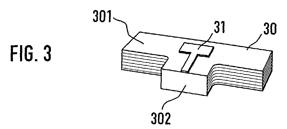
- Figure 3 illustrates a stand-alone piece 30 according to the present invention.
- Stand alone piece 30 is a piece of dielectric comprising on its surface a microstrip line termination 31.
- the dielectric is chosen to be transparent to microwave possible materials are 25N substrate form the company Arlon or RO4003 from the company Rogers Corp.
- the used dielectric material depends preferably of the frequency range generated and transported on motherboard 20.
- the shape of stand alone piece is preferably and an arrangement of two parallelepipeds : the first one 301 having a basis shape substantially identical to the shape of hole 22 and the second one 302 supporting the extremity of microstrip line termination 301 which have to be connected to the extremity of the microstrip line termination 201 located on motherboard 20.
- the other extremity of microstrip line termination on stand alone piece 30 being substantially located at the center of first parallelepiped 301.
- the surface of parallelepiped 301 opposite to the surface supporting microstrip line termination 31 as well as the surfaces perpendicular to this surface are metallized. This results in that stand alone piece has also the function of the closed extremity of waveguide 21.
- the height h of both parallelepipeds 301, 302 is chosen so as to propagate the microwave in waveguide 21 without generating reflections due to characteristic impedance discontinuity (mismatch) at the transition between waveguide 21 and the microstrip line. These reflections would induce losses and degrade the system behavior.
- stand alone piece 30 presented on figure 3 is I/w/h: 6,5mmm/5mm/1,5mm. A person skilled in the art will understand that any other dimension may be selected or adapting stand alone piece 30 to a particular motherboard20 / waveguide21 arrangement.
- stand alone piece 30 can be chosen a different way to fulfil the same function i.e. supporting and bringing microstrip line termination 31 at the center of waveguide 21 and optionally acting as a closed extremity of waveguide 21.
- the shape of stand alone piece 30 depends preferably on the shape of the section of waveguide 21.
- Figure 4 represents stand-alone piece 30 mounted on motherboard 20 according to the present invention.
- Stand alone piece 30 is mounted on motherboard 20 on hole 22 so that microstrip line termination 31 coincides with the extremity of microstip line 201.
- Stand alone piece 30 is preferably fixed on motherboard 20 by using glue.
- Stand-alone piece 30 will preferably be put in a tap and reel feeding system when manipulated in a Surface Mounted Technology assembly line.
- Several stand-alone pieces 30 are preferably manufactured together as attached to a panel , the microstrip line terminations and the metal layer being automatically applied to each stand alone pieces attached to the panel. The stand-alone pieces can after manufacture be separated from the panel for further use.
- the metallized surface on the side of stand alone piece 30 contacts with the metallized rubban 41 around hole 22 perforated with metallized holes 411.
- Waveguide 21 contacts also with these metallized holes on the other side of motherboard 20.
- the metallized surface on the top an on the sides of stand-alone piece 30 cat as the closed extremity of waveguide 21.
- the metallized sides of stand alone piece 30 can be replaced by a fence of metallized holes along each of the four sides. Using holes increases the processing yields since it is difficult to deposit a metal layer on a large surface of dielectric material.
- a multilayer mother board is used.
- Each layer of the mother board comprising surface mounted corposants and a microstrip line ending at the edge of hole 22. It is important to ensure the electric contact between all extremities of microstrip lines at the edge of hole 22 and microstrip line termination 31.
- a solution to this problem consists in providing an electric contact linking all extremities of the microstrip lines belonging to the different mother board layers and connecting this electric contact with microstrip line termination 31.
- microstrip line terminations can be supported on stand alone piece 30, each microstrip line termination being connected to the extremity of a microstrip line of a different layer of the motherboard.
- An arrangement comprising a stand-alone piece according to the invention used as transition between a microstrip line on a flat board an a waveguide may preferably be used in a microwave radio transceiver, the waveguide propagating a microwave to/from an antenna and the microstrip line propagating the microwave to/from the input/output stage of the transceiver.
Landscapes
- Waveguides (AREA)
- Non-Reversible Transmitting Devices (AREA)
Abstract
The invention relates to a arrangement comprising:
- a flat board comprising microwave integrated modules and at least one microstrip line for guiding a signal on said flat board, and
- a waveguide for guiding the signal out of the flat board.
According to the present invention the flat board is perforated at
the intersection between the flat board and the waveguide, a stand-alone
piece comprising a microstrip line termination is adjusted over the
perforation, the microstrip line termination coinciding with the
extremity of one microstrip line on the flat board.
Description
The present invention relates to microwave transmission and more
precisely to a transition between a microstrip line and a rectangular
waveguide both dedicated to transmit a microwave signal.
The output stage of a microwave radio transmitter comprises
integrated microwave modules consisting microwave components mounted
on the surface of a "flat" motherboard using preferably the M-SMT
technology (microwave surface mount technology). Such components may
be amplifiers, mixers, attenuators.
The microwave signals generated in the components are usually
propagated through microstrip lines between the different components.
Microstrip lines have the advantage to be flat and require not a lot of
space.
The signal has further to be propagated from the motherboard to
the antenna of the microwave radio transmitter. Contrary to the
motherboard where the signal is localised on a microstrip line, a
rectangular waveguide forwards the signal to the antenna. The transition
between the microstrip line and the rectangular waveguide should be
properly adapted to avoid signal loss at the transition which would create
unwanted interference in the microwave module.
A known solution for providing an appropriate transition between a
microstrip line located on a motherboard and a rectangular waveguide is
described in figure 1. Figure 1a is a top elevation view of the mother board
while figure 1b is a side view of the transition between the microstrip line
and the rectangular waveguide along line A-A.
In this arrangement, the rectangular waveguide 11 is perpendicular
to the plane of the motherboard 10 as shown on the view illustrated on
figure 1b.
The extremity of a microstrip line 101 printed on the motherboard
10 is the transition point to the rectangular waveguide 10 and is
substantially located at the center of the section of rectangular waveguide
11.
A cover 12 located over motherboard 10 on the other side of
motherboard 10 as rectangular waveguide 11 acts as closed extremity of
rectangular waveguide 11. For this purpose conductive paste is deposited
over the edge of the conductive cover acting as closed extremity of the
waveguide. The conductive paste is in contact with metallized holes
perforated on the motherboard. The metallized holed ensure the contact
with the rectangular waveguide 11.
The material of motherboard 10 being namely transparent to
microwaves usually having a frequency roughly between 1 GHz and 30GHz
and is thin enough not to prevent the propagation of the microwave signal
through it.
This arrangement presents a drawback for multilayer motherboards
used in order to increase the number of components on a single
motherboard. Several layers using the microwave surface mount technology
being assembled together. Several layers of substrate render the
motherboard thicker. As a consequence, the signal is attenuated at the
transition to the rectangular waveguide. This attenuation reduce the
performance of the microwave module.
A particular object of the present invention is to provide an
arrangement for a transition between a microstrip line and a waveguide
which reduce the signal attenuation at the transition point.
Other objects of the invention is to provide a radio transmitter such
a such arrangement as well as a method for manufacturing such an
arrangement.
These objects, and others that appear below, are achieved by an
arrangement according to claim 1 and a microwave radio transceiver
according to claim 8.
According to the present invention, a perforation (hole) is made in
the motherboard at the place corresponding to the extremity of the
waveguide. This hole prevents the thick substrate from attenuating the
signal at the transition between the microstrip and the waveguide.
Moreover, a stand-alone piece of dielectric having a microstrip line
termination is placed above the hole and acts as the termination of the
microtrip line.
The stand alone piece must be adjusted on the motherboard so that
the contact is ensured between the extremity of the microsprip line at the
edge of the hole and the microstrip line termination on the stand-alone
piece of dielectric.
The method according to the present invention presents the
advantage to increase the performance of the microwave module
comprising a transition according to the present invention in that the
dielectric material can be chosen to be as transparent a possible to the
microwave especially for multilayer integrated microwave circuits.
In a preferred embodiment of the present invention, the stand-alone
piece of dielectric act additionally as closed extremity of the
rectangular waveguide. For this purpose, the piece of dielectric is metallized
on its top and on its sides.
This embodiment further presents the advantage to reduce the
complexity of manufacturing the microwave module in that the cover needs
no more to ensure a perfect electric contact with the waveguide.
Further advantageous features of the invention are defined in the
dependent claims.
Other characteristics and advantages of the invention will appear
on reading the following description of a preferred embodiment given by
way of non-limiting illustrations, and from the accompanying drawings, in
which:
- Figure 1 shows a prior art arrangement for ensuring a transition between a microstrip line and a rectangular waveguide;
- Figure 2 shows a motherboard presenting a perforation according to the present invention;
- Figure 3 illustrates a stand-alone piece according to the present invention;
- Figure 4 represents the stand-alone piece mounted on the motherboard according to the present invention.
Figure 1 has already been described in connection with prior art.
Figure 2 shows a motherboard presenting a hole according to the
present invention.
Figure 2a is a top elevation view of a motherboard 20 while figure
2b is a side view of motherboard 20 and a waveguide 21 perpendicular to
the plane of the motherboard 20 along line B-B.
In this embodiment, the waveguide is chosen rectangular. The
invention is however not limited to a rectangular waveguide. Circular
waveguide or any other type of hollow waveguide or filled in with a
dielectric can be used as well.
In this arrangement, a hole 22 having substantially the shape of
waveguide 21section is perforated on the part of motherboard 20
coinciding with the intersection with waveguide 21.
A microstrip line 201 printed on motherboard 20 transports the
microwave between components 202 located on motherboard 20 and ends
at the edge of hole 22.
substantially located at the center of the section ofrectangular
waveguide 11.
substantially located at the center of the section of
A conductive cover (not represented) can be put above
motherboard 20. A conductive paste can be deposited between the
conductive cover and metallized holes 203 perforated on motherboard 20.
The metallized holes ensure the electric contact with rectangular waveguide
11 and a cover (as cover 12 shown on figure 1 b) can act as closed
extremity of waveguide 11.
Figure 3 illustrates a stand-alone piece 30 according to the present
invention.
Stand alone piece 30 is a piece of dielectric comprising on its
surface a microstrip line termination 31. The dielectric is chosen to be
transparent to microwave possible materials are 25N substrate form the
company Arlon or RO4003 from the company Rogers Corp. The used
dielectric material depends preferably of the frequency range generated
and transported on motherboard 20.
The shape of stand alone piece is preferably and an arrangement
of two parallelepipeds : the first one 301 having a basis shape substantially
identical to the shape of hole 22 and the second one 302 supporting the
extremity of microstrip line termination 301 which have to be connected to
the extremity of the microstrip line termination 201 located on motherboard
20. The other extremity of microstrip line termination on stand alone piece
30 being substantially located at the center of first parallelepiped 301.
In a preferred embodiment of the invention, the surface of
parallelepiped 301 opposite to the surface supporting microstrip line
termination 31 as well as the surfaces perpendicular to this surface are
metallized. This results in that stand alone piece has also the function of the
closed extremity of waveguide 21.
In this embodiment, the height h of both parallelepipeds 301, 302
is chosen so as to propagate the microwave in waveguide 21 without
generating reflections due to characteristic impedance discontinuity
(mismatch) at the transition between waveguide 21 and the microstrip line.
These reflections would induce losses and degrade the system behavior.
The size of stand alone piece 30 presented on figure 3 is I/w/h:
6,5mmm/5mm/1,5mm. A person skilled in the art will understand that any
other dimension may be selected or adapting stand alone piece 30 to a
particular motherboard20 / waveguide21 arrangement.
It will be clear for a person skilled in the art, that the shape of stand
alone piece 30 can be chosen a different way to fulfil the same function i.e.
supporting and bringing microstrip line termination 31 at the center of
waveguide 21 and optionally acting as a closed extremity of waveguide 21.
The shape of stand alone piece 30 depends preferably on the shape of the
section of waveguide 21.
Figure 4 represents stand-alone piece 30 mounted on motherboard
20 according to the present invention. Stand alone piece 30 is mounted on
motherboard 20 on hole 22 so that microstrip line termination 31 coincides
with the extremity of microstip line 201. Stand alone piece 30 is preferably
fixed on motherboard 20 by using glue. Stand-alone piece 30 will
preferably be put in a tap and reel feeding system when manipulated in a
Surface Mounted Technology assembly line. Several stand-alone pieces 30
are preferably manufactured together as attached to a panel , the
microstrip line terminations and the metal layer being automatically applied
to each stand alone pieces attached to the panel. The stand-alone pieces
can after manufacture be separated from the panel for further use.
In a preferred embodiment of the present invention, the metallized
surface on the side of stand alone piece 30 contacts with the metallized
rubban 41 around hole 22 perforated with metallized holes 411.
Waveguide 21 contacts also with these metallized holes on the other side of
motherboard 20. As a consequence the metallized surface on the top an on
the sides of stand-alone piece 30 cat as the closed extremity of waveguide
21. In another embodiment of the present invention, the metallized sides of
stand alone piece 30 can be replaced by a fence of metallized holes along
each of the four sides. Using holes increases the processing yields since it is
difficult to deposit a metal layer on a large surface of dielectric material.
In a preferred embodiment of the present invention, a multilayer
mother board is used. Each layer of the mother board comprising surface
mounted corposants and a microstrip line ending at the edge of hole 22. It
is important to ensure the electric contact between all extremities of
microstrip lines at the edge of hole 22 and microstrip line termination 31. A
solution to this problem consists in providing an electric contact linking all
extremities of the microstrip lines belonging to the different mother board
layers and connecting this electric contact with microstrip line termination
31.
In a further embodiment of the present invention, several microstrip
line terminations can be supported on stand alone piece 30, each
microstrip line termination being connected to the extremity of a microstrip
line of a different layer of the motherboard.
An arrangement comprising a stand-alone piece according to the
invention used as transition between a microstrip line on a flat board an a
waveguide may preferably be used in a microwave radio transceiver, the
waveguide propagating a microwave to/from an antenna and the
microstrip line propagating the microwave to/from the input/output stage of
the transceiver.
Claims (8)
- Arrangement comprising :said arrangement being characterised in that :a flat board (20) comprising microwave integrated modules (202) and at least one microstrip line (301) for guiding a signal on said flat board (20) anda waveguide (21) for guiding said signal out of said flat board (20),said flat board (20) is perforated (22) at the intersection between said flat board (20) and said waveguide (21), a stand-alone piece of dielectric (30) comprising a microstrip line termination (31) and being adjusted over said perforation (22) of said flat board (20), said microstrip line termination (31) coinciding with the extremity of said microstrip line (201) on said flat board (20).
- Arrangement according to claim 1, characterised in that said stand alone piece of dielectric (30) comprises metallized surfaces in contact with said flat board (20) and coinciding with the waveguide extremity (21) in contact with said flat board (20), said metallized surfaces acting as closed extremity of said waveguide (21).
- Arrangement according to claim 1, characterised in that, said stand-alone piece (30) is made out of a dielectric substantially transparent to microwaves.
- Arrangement according to claim 1, characterised in that said stand alone piece of dielectric (30) has the shape of two assembled parallelepipeds (301, 302), a first one (301) having substantially the shape of said perforation (22), a second (302) being used to fix said stand alone piece of dielectric (30) on said flat board (20).
- Arrangement according to claim 1, characterised in that said flat board comprises surface mount technology components.
- Arrangement according to claim 1, characterised in that said flat board is a multilayer flat board comprising at least two layer of surface mounted components.
- Arrangement according to claim 1, characterised in that it is part of a microwave radio transceiver, said waveguide propagating a microwave between said antenna and said flat board supporting the input/output stage of said transceiver.
- Microwave radio transceiver comprising an arrangement according to claim 1.
Priority Applications (3)
| Application Number | Priority Date | Filing Date | Title |
|---|---|---|---|
| EP02360048A EP1333526A1 (en) | 2002-01-30 | 2002-01-30 | Transition between a microstrip line and a waveguide |
| CN03102243.XA CN1438731A (en) | 2002-01-30 | 2003-01-28 | Conversion between micro-band and rectangular wavegaide |
| US10/352,099 US20030141940A1 (en) | 2002-01-30 | 2003-01-28 | Transition between a microstrip line and a rectangular waveguide |
Applications Claiming Priority (1)
| Application Number | Priority Date | Filing Date | Title |
|---|---|---|---|
| EP02360048A EP1333526A1 (en) | 2002-01-30 | 2002-01-30 | Transition between a microstrip line and a waveguide |
Publications (1)
| Publication Number | Publication Date |
|---|---|
| EP1333526A1 true EP1333526A1 (en) | 2003-08-06 |
Family
ID=8185763
Family Applications (1)
| Application Number | Title | Priority Date | Filing Date |
|---|---|---|---|
| EP02360048A Withdrawn EP1333526A1 (en) | 2002-01-30 | 2002-01-30 | Transition between a microstrip line and a waveguide |
Country Status (3)
| Country | Link |
|---|---|
| US (1) | US20030141940A1 (en) |
| EP (1) | EP1333526A1 (en) |
| CN (1) | CN1438731A (en) |
Families Citing this family (7)
| Publication number | Priority date | Publication date | Assignee | Title |
|---|---|---|---|---|
| EP1820236B1 (en) * | 2004-11-30 | 2009-04-01 | Telefonaktiebolaget LM Ericsson (publ) | A transmission arrangement |
| US7752911B2 (en) * | 2005-11-14 | 2010-07-13 | Vega Grieshaber Kg | Waveguide transition for a fill level radar |
| US7420436B2 (en) * | 2006-03-14 | 2008-09-02 | Northrop Grumman Corporation | Transmission line to waveguide transition having a widened transmission with a window at the widened end |
| WO2008069714A1 (en) * | 2006-12-05 | 2008-06-12 | Telefonaktiebolaget Lm Ericsson (Publ) | A surface-mountable waveguide arrangement |
| JP6369394B2 (en) * | 2015-06-08 | 2018-08-08 | 住友電気工業株式会社 | Transmission line-waveguide converter |
| US10403954B2 (en) * | 2017-12-30 | 2019-09-03 | Texas Instruments Incorporated | Printed circuit board with substrate-integrated waveguide transition |
| EP3955376B1 (en) * | 2020-08-12 | 2025-01-01 | VEGA Grieshaber KG | Waveguide coupling device for a radar sensor |
Citations (3)
| Publication number | Priority date | Publication date | Assignee | Title |
|---|---|---|---|---|
| EP0788183A2 (en) * | 1992-11-10 | 1997-08-06 | Sony Corporation | Waveguide-microstrip line mode transformer for microwave apparatus |
| EP0920071A2 (en) * | 1997-11-26 | 1999-06-02 | TRW Inc. | Millimeter-wave LTCC package |
| US5912598A (en) * | 1997-07-01 | 1999-06-15 | Trw Inc. | Waveguide-to-microstrip transition for mmwave and MMIC applications |
-
2002
- 2002-01-30 EP EP02360048A patent/EP1333526A1/en not_active Withdrawn
-
2003
- 2003-01-28 US US10/352,099 patent/US20030141940A1/en not_active Abandoned
- 2003-01-28 CN CN03102243.XA patent/CN1438731A/en active Pending
Patent Citations (3)
| Publication number | Priority date | Publication date | Assignee | Title |
|---|---|---|---|---|
| EP0788183A2 (en) * | 1992-11-10 | 1997-08-06 | Sony Corporation | Waveguide-microstrip line mode transformer for microwave apparatus |
| US5912598A (en) * | 1997-07-01 | 1999-06-15 | Trw Inc. | Waveguide-to-microstrip transition for mmwave and MMIC applications |
| EP0920071A2 (en) * | 1997-11-26 | 1999-06-02 | TRW Inc. | Millimeter-wave LTCC package |
Also Published As
| Publication number | Publication date |
|---|---|
| CN1438731A (en) | 2003-08-27 |
| US20030141940A1 (en) | 2003-07-31 |
Similar Documents
| Publication | Publication Date | Title |
|---|---|---|
| CA2712949C (en) | A radio frequency circuit board topology | |
| JP2005045815A (en) | Millimeter-wave signal conversion device | |
| AU2010329983A1 (en) | Microwave transition device between a microstrip line and a rectangular waveguide | |
| CN113347780B (en) | A fin wire structure composed of a multi-layer circuit board | |
| US9054404B2 (en) | Multi-layer circuit board with waveguide to microstrip transition structure | |
| JP2002198709A (en) | High frequency wiring board | |
| US20050179600A1 (en) | Low-loss printed circuit board antenna structure and method of manufacture thereof | |
| EP3879640B1 (en) | Coaxial connector and substrate equipped with coaxial connector | |
| EP1333526A1 (en) | Transition between a microstrip line and a waveguide | |
| JPWO2008146535A1 (en) | Terminator | |
| US8227707B2 (en) | Coaxial connector mounted circuit board | |
| CN115207591B (en) | Strong coupling strip line and microwave element containing the same | |
| EP2897216A1 (en) | Systems and methods for a suspended stripline antenna driving system | |
| JP2020506603A (en) | Transmission line-waveguide transition device | |
| US11658377B2 (en) | Substrate-mountable electromagnetic waveguide | |
| US7355496B2 (en) | Finline type microwave band-pass filter | |
| JP2005051330A (en) | Connection structure between dielectric waveguide line and high-frequency transmission line, high-frequency circuit board using the same, and package for mounting high-frequency element | |
| US4085390A (en) | Symmetrical stripline package | |
| US20090267711A1 (en) | High frequency circuit | |
| US20040145427A1 (en) | Quadrature hybrid low loss directional coupler | |
| JP3008939B1 (en) | High frequency circuit board | |
| EP0500949A1 (en) | Microwave circuit | |
| JP3464108B2 (en) | Feeding structure of laminated dielectric waveguide | |
| CN114552155B (en) | Dual-mode transmission line | |
| JP6964824B2 (en) | Converter and antenna device |
Legal Events
| Date | Code | Title | Description |
|---|---|---|---|
| GRAH | Despatch of communication of intention to grant a patent |
Free format text: ORIGINAL CODE: EPIDOS IGRA |
|
| PUAI | Public reference made under article 153(3) epc to a published international application that has entered the european phase |
Free format text: ORIGINAL CODE: 0009012 |
|
| 17P | Request for examination filed |
Effective date: 20021114 |
|
| AK | Designated contracting states |
Designated state(s): AT BE CH CY DE DK ES FI FR GB GR IE IT LI LU MC NL PT SE TR |
|
| AX | Request for extension of the european patent |
Extension state: AL LT LV MK RO SI |
|
| STAA | Information on the status of an ep patent application or granted ep patent |
Free format text: STATUS: THE APPLICATION IS DEEMED TO BE WITHDRAWN |
|
| 18D | Application deemed to be withdrawn |
Effective date: 20030917 |