EP1333496A2 - Semiconductor device for RF signal switching with high isolation layout for the signal lines - Google Patents
Semiconductor device for RF signal switching with high isolation layout for the signal lines Download PDFInfo
- Publication number
- EP1333496A2 EP1333496A2 EP03000962A EP03000962A EP1333496A2 EP 1333496 A2 EP1333496 A2 EP 1333496A2 EP 03000962 A EP03000962 A EP 03000962A EP 03000962 A EP03000962 A EP 03000962A EP 1333496 A2 EP1333496 A2 EP 1333496A2
- Authority
- EP
- European Patent Office
- Prior art keywords
- semiconductor device
- signal
- output
- input
- mounting board
- Prior art date
- Legal status (The legal status is an assumption and is not a legal conclusion. Google has not performed a legal analysis and makes no representation as to the accuracy of the status listed.)
- Withdrawn
Links
Images



Classifications
-
- H—ELECTRICITY
- H10—SEMICONDUCTOR DEVICES; ELECTRIC SOLID-STATE DEVICES NOT OTHERWISE PROVIDED FOR
- H10W—GENERIC PACKAGES, INTERCONNECTIONS, CONNECTORS OR OTHER CONSTRUCTIONAL DETAILS OF DEVICES COVERED BY CLASS H10
- H10W44/00—Electrical arrangements for controlling or matching impedance
- H10W44/20—Electrical arrangements for controlling or matching impedance at high-frequency [HF] or radio frequency [RF]
-
- H—ELECTRICITY
- H01—ELECTRIC ELEMENTS
- H01P—WAVEGUIDES; RESONATORS, LINES, OR OTHER DEVICES OF THE WAVEGUIDE TYPE
- H01P1/00—Auxiliary devices
- H01P1/10—Auxiliary devices for switching or interrupting
- H01P1/15—Auxiliary devices for switching or interrupting by semiconductor devices
-
- H—ELECTRICITY
- H10—SEMICONDUCTOR DEVICES; ELECTRIC SOLID-STATE DEVICES NOT OTHERWISE PROVIDED FOR
- H10W—GENERIC PACKAGES, INTERCONNECTIONS, CONNECTORS OR OTHER CONSTRUCTIONAL DETAILS OF DEVICES COVERED BY CLASS H10
- H10W44/00—Electrical arrangements for controlling or matching impedance
- H10W44/20—Electrical arrangements for controlling or matching impedance at high-frequency [HF] or radio frequency [RF]
- H10W44/203—Electrical connections
- H10W44/216—Waveguides, e.g. strip lines
Definitions
- the present invention relates to a high-isolation semiconductor device and, more particularly, to a high-isolation semiconductor device suitable for use in a satellite television receiver.
- a switching device is often used for switching a plurality of high-frequency signals, or radio-frequency signals (RF signals), supplied through respective channels to deliver a selected one of the RF signals to each of a plurality of receivers.
- the switching device for the RF signais is generally implemented by a matrix switch having a plurality of inputs and a plurality of outputs, wherein a selected one of the inputs can be coupled to each of the outputs.
- Fig. 7 shows a typical circuit configuration of a switching device 500 for receiving two input RF signals, signal A and signal B, to deliver a selected one of the input signals to each of two receivers 80 and 81.
- the switching device 500 is implemented by a 2 ⁇ 2 matrix switch having two inputs and two outputs, or two SPDT (single-pole-double-throw) switches.
- Each of the receivers 80 and 81 is connected to a corresponding output terminal of the switching device 500 to receive one of the RF signals, signal A and signal B, independently of each other.
- the matrix switches incorporated in a communication SWIC or communication LSI are generally implemented by transistors, such as a junction FET, or a pin-junction photo-diode.
- the communication SWICs for example, include a SPDT SWIC having a plurality of separate SPDTs which are the minimum switch units, and a twin-SWIC having a plurality of SPDT pairs, each pair being connected in parallel.
- the SWIC is mounted on a mounting board having a dielectric substrate and patterned interconnections formed on top and bottom surfaces of the dielectric substrate.
- the twin-SWIC for example, may include interconnections therein and may be received in a package together with the interconnections.
- the performance of a matrix switch with respect to the isolation characteristic is estimated by an isolation D/U (desired-to-undesired) ratio of each signal line receiving a desired output signal, which is calculated by the power ratio of the desired signal component to the undesired signal component, both the components being included in the output signal. It is desired that transmitters and receivers used in the up-to-date satellite broadcasting system have an isolation D/U ratio as high as 40dB or above.
- the isolation D/U ratio as high as 40dB or above can be achieved in a SWIC itself as a separate unit by suitably selecting the constituent elements, circuit configuration, circuit constants and layout pattern of the SWIC.
- a plurality of SWICs are connected together by signal lines for achieving a matrix switch having a plurality of inputs and a plurality of outputs, there are crossing points between these signal lines which transmit the RF signals.
- This makes it difficult to achieve a high isolation D/U ratio with respect to the signal lines, whereby the switching device cannot achieve a higher isolation characteristic as a whole.
- the signal line for transmitting the signal A and the signal line for transmitting the signal B cross each other at the crossing point C1, wherein the signal leakage arises therebetween to degrade the isolation D/U ratio of the signal lines.
- a 2 ⁇ 2 matrix switch for example, is generally implemented by mounting a plurality of SPDT SWICs or twin-SWICs on a mounting board having patterned interconnections or mounting a single 2 ⁇ 2 matrix SWIC on such a mounting board.
- a crossing point arises between RF signal lines on the mounting board
- a crossing point arises between RF signal lines within the 2 ⁇ 2 matrix SWIC.
- the signal leakage should be suppressed by enlarging the distance between the RF signal lines and/or reducing the projected area of the opposing RF signal lines at the crossing point.
- Fig. 8A is the top plan view of a switching device implemented by a single SWIC including a 2 ⁇ 2 matrix switch
- Fig. 8B is the sectional view of the crossing point shown in Fig. 8A.
- the switching device includes RF signal lines which include a plated signal line 46 plated with gold and overlying a dielectric film (oxide film) 42, and a metallic signal line 47 underlying the dielectric film 42, wherein the signal lines 46 and 47 oppose each other at the crossing point C1 with an intervention of the dielectric film 42.
- the dielectric film 42 has a small thickness on the order of micrometers, whereby the distance between the RF signal lines 46 and 47 is small and a large cross-talk may arise therebetween. Assuming that the projected area of the opposing RF signal line is around a several-micrometer square, the level of the cross-talk between the RF signal lines is around 30dB, which is not negligible for the switching device.
- Figs. 9A and 9B show, similarly to Figs. 8A and 8B, another conventional switching device 600 implemented by two SWICs 10 and 11 each including SPDT switch and mounted on a common mounting board 40.
- metallic signal lines 47 oppose each other with an intervention of the mounting board 40 having a thickness of around 1mm or below.
- the RF signal lines 47 on the mounting board 40 have a characteristic impedance of 50 ⁇
- the RF signal lines 47 have a width of around 1mm, assuming that the mounting board 40 has a dielectric constant £ of 3.38 and a thickness of 0.51mm, for example. This may cause a significant cross-talk level between the RF signal lines 47, e.g., an isolation D/U ratio around 30dB with respect to the RF signal lines 47.
- the mounting board 40 has a micro-strip line structure, there arises a mismatching of the characteristic impedance due to the fact that a ground plane cannot be provided at the crossing point C1 on the surface of the mounting board 40 opposite to the surface on which the subject RF signal line 47 is formed.
- Figs. 10A and 10B show, similarly to Figs. 8A and 8B, another conventional switching device 700 implemented by two SWICs 10 and 11 each including SPDT switch and mounted on a common mounting board, which includes a pair of dielectric substrates 40 and a ground plane 80 sandwiched therebetween.
- RF signal lines 47 oppose each other with an intervention of the mounting board including the ground plane 80 and the dielectric substrates 40.
- This structure allows significant reduction of the cross-talk level between the RF signal lines 47 and suppresses the mismatching of the characteristic impedance.
- the mounting board has a larger thickness and the fabrication cost thereof is higher.
- Figs. 11 is a top plan view of another conventional switching device 800 implemented by a twin-SWIC 20.
- a semi-rigid cable 50 is used as a part of one of the RF signal lines 47 and raised from the mounting board 40 at the crossing point C1.
- This structure reduces the cross-talk between the RF signal lines 47; however, the junction for connecting the signal line 47 on the mounting board 40 and the semi-rigid cable 50 causes miss-matching of the characteristic impedance and thus degrades the signal characteristics, such as a return loss.
- arrangement of the semi-rigid cable 50 above the mounting board 40 raises the costs for the switching device 800.
- the conventional techniques for the switching device do not achieve a high isolation D/U ratio in the switching device without involving the miss-matching of the characteristic impedance and/or raising the fabrication costs.
- the present invention provides a semiconductor device including at least one integrated circuit (IC) and a mounting board having a top surface for mounting thereon the IC at a bottom surface of the IC, the mounting board including a dielectric substrate, first and second input lines formed on the dielectric substrate for transferring first and second input signals, respectively, to the IC, and first and second output lines formed on the dielectric substrate for transferring first and second output signals, respectively, generated by the IC based on the first and second input signals, wherein the mounting board has no crossing point between the first input line and the second input line on either side of the dielectric substrate.
- IC integrated circuit
- the absence of the crossing point on either side of the mounting board reduces the cross-talk between the first input line and the second input line, whereby the semiconductor device has a higher isolation characteristic.
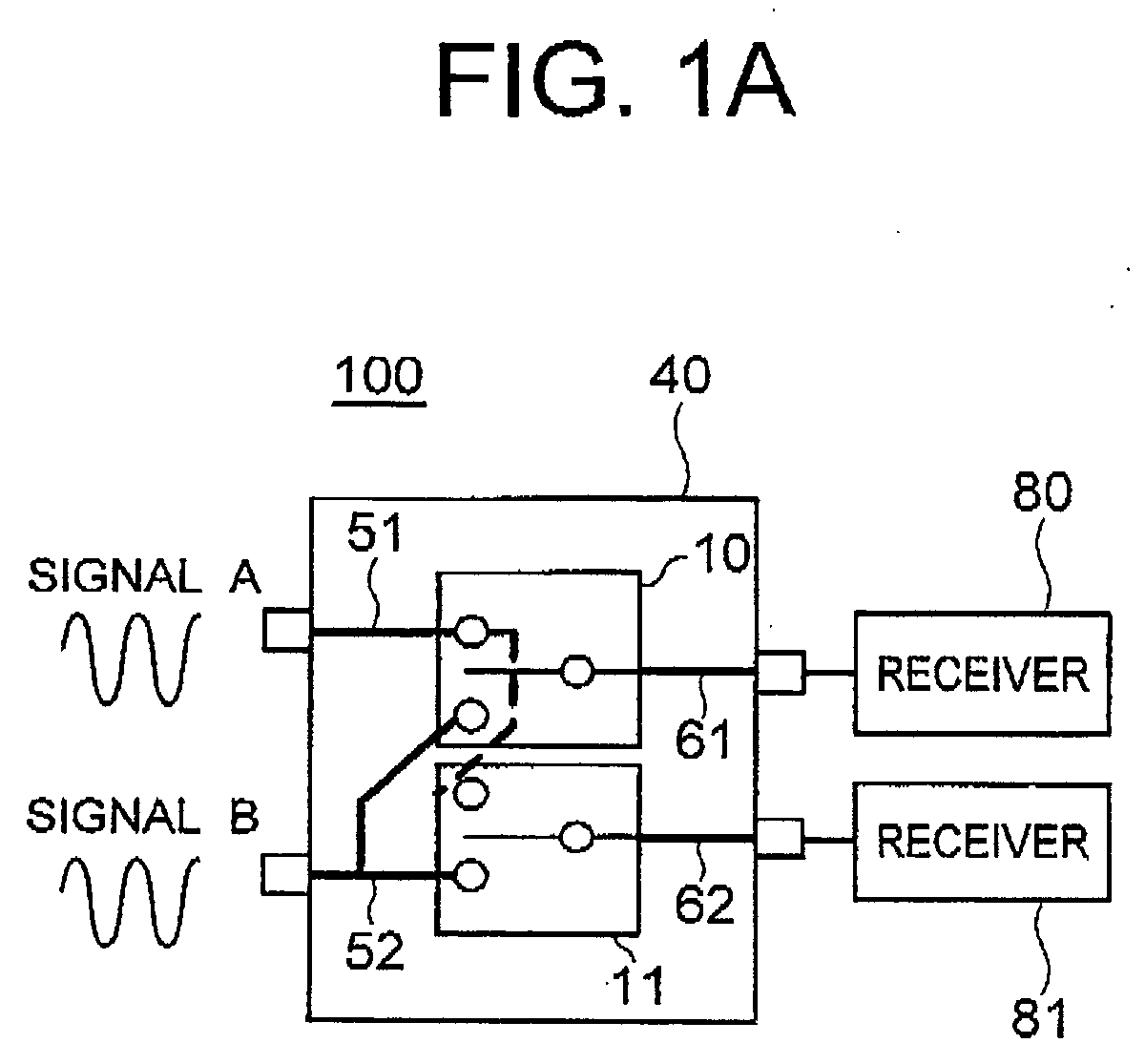
- a switching device generally designated by numeral 100, according a first embodiment of the present invention includes a mounting board 40 made of insulator substrate and including therein patterned signal lines 51, 52, 61 and 62, and a matrix switch implemented by a pair of SPDT SWICs 10 and 11 mounted on the mounted board 40.
- the signal lines shown by solid lines are formed on the top surface of the dielectric substrate, wherein the signal line shown by a dotted line is formed on the bottom surface of the dielectric substrate.
- the switching device 100 receives at the inputs thereof RF signals, or signal A and signal B, to deliver one of the RF signals to each of receivers 80 and 81 via signal lines 51, 52, 61 and 62 and SPDT SWICs 10 and 11. That is, the receivers 80 and 81 receive one of the signals A and B independently of each other by the function of the switching device.
- SPDT SWIC 10 switches the RF signals for receiver 80
- SPDT SWIC 11 switches the RF signals for receiver 81.
- the signal lines 51 and 52 are patterned on the mounting board 40 so that the signal lines 51 and 52 have no crossing point therebetween on each of the top and bottom surfaces of the insulator substrate 40.
- through-holes 41 penetrate the mounting board 40 to connect a portion of the signal line 51 formed on the top surface of the mounting board 40 to another portion of the signal line 51 formed on the bottom surface.
- the RF signal lines are arranged in the order of signal line 51, signal line 52, signal line 51 and signal line 52. This arrangement is employed because the distance between the signal lines 51 and 52 can be secured to a desired extent by sufficiently separating the SWICs 10 and 11 from each other.
- ground conductors 80 each configuring a ground plane are formed on the top and bottom surfaces of the mounting board 40 so as to oppose the signal lines 51 and 52, respectively, formed on the bottom and top surface of the mounting board 40. That is, the configuration of the present embodiment wherein there is no crossing point on either surface of the mounting board 40 allows all the signal lines 51, 52, 61 and 62 to be associated with ground conductors 80 formed on the opposite surface of the mounting board 40.
- the SPDT SWICs 10 and 11 are encapsulated in a mold resin 45 which is mounted on the top surface of the mounting board 40.
- a lead frame 44 is interposed between the mold resin 45 and a GaAs substrate 43, on which signal amplifiers etc. are formed for processing the RF signals.
- the plated signal lines 46 plated with gold and connected to the GaAs substrate 43 are disposed on a dielectric film 43 formed on the GaAs substrate 20.
- the metallic signal lines 47 formed on the bottom surface of the mounting board 40 oppose the plated signal lines 46 on the dielectric film 43 with an intervention of the dielectric film 42, GaAs substrate 43, lead frame 44, mold resin 45 and mounting board 40, whereby the distance between the signal lines 47 and the signal lines 46 is on the order of millimeters, and thus is sufficient for suppressing the cross-talk therebetween.
- the signal line 46 is also disposed sufficiently apart from other signal lines formed on the, top surface of the mounting board 40. Since the signal lines formed within the SPDT SWICs have a smaller width, the cross-talk between the signal lines in the SWICs is smaller due to the smaller opposing area.
- the switching device 100 of the present embodiment has an isolation D/U ratio as high as 40dB or higher, and thus the cross-talk between the signal line 51 and the signal line 52 in Fig. 1 can be suppressed to a suitable level.
- these signal lines 51, 52, 61 and 62 can be formed in a micro-strip line structure, whereby excellent impedance matching can be obtained therein. Further, since these signal lines can be formed by a photographic patterning technique, an additional material or an additional assembly process is not needed, which reduces the fabrication costs for the switching device 100.
- a switching device generally designated by numeral 200, according to a second embodiment of the present invention is implemented by a matrix switch formed by a twin-SWIC 20 including two SPDT switches therein.
- the single IC 20 employed reduces the man-hours for fabrication.
- the RF signal lines are arranged at the input side of the SWIC 20 in the order of signal line 52, signal line 51, signal line 51 and signal line 52. This arrangement is employed for reducing the cross-talk between the signal lines 51 and 52 to achieve a higher isolation D/U ratio in the case of the single IC 20.
- the signal line 51 has a portion formed on the bottom surface of the mounting board 40 for avoiding occurrence of a crossing point on the top surface of the mounting substrate 40.
- a switching device receives four RF signals, signal A to signal D to deliver a selected one of the RF signals to each of two receivers 80 and 81.
- the switching device 300 is implemented by a pair of twin-SWICs 20 and 21 and a pair of SPDT SWICs 10 and 11, all of which are mounted on a single mounting board 40.
- Twin SWIC 20 selects one of the signals A and B received via signal lines 51 and 52, respectively, and delivers the selected signal to a first input of each of the SPDT SWICs 10 and 11 via a signal line 71 or 73.
- Twin SWIC 21 selects one of the signals C and D received via signal lines 53 and 54, respectively, and delivers the selected signal to a second input of each of the SPDT SWICs 10 and 11 via a signal line 72 or 74.
- Each of the SPDT SWICs 10 and 22 selects the RF signal received at the first input or the second input to deliver the selected RF signal to a corresponding receiver 80 or 81.
- each of the receivers 80 and 81 independently receives any one of the RF signals A to D by the function of the switching device 300.
- the arrangement of the signal lines 51 and 52 as well as the arrangement of the signal lines 53 and 54 on the mounting board 40 shown in Fig. 5B is similar to the arrangement of the signal lines 51 and 52 shown in Fig. 4B.
- the signal lines 71 to 74 are arranged so that these signal lines 71 to 74 do not have a crossing point therebetween on either surface of the mounting board 40, as shown in Fig. 5B. This allows a higher isolation D/U ratio, as well.
- a switching device generally designated by numeral 400, according to a fourth embodiment of the present invention includes a matrix switch implemented by a pair of 2 ⁇ 2 SWICs 30 and 31 and a pair of SPDT SWICs 10 and 11, all of which are mounted on a mounting board 40.
- the 2 ⁇ 2 SWICs 30 31 have therein a crossing point between the RF signal lines.
- the signal lines in the 2 ⁇ 2 SWICs 30 and 31 have a lower isolation D/U ratio, due to the cross-talk between signal A and signal B as well as between signal C and signal D in the illustrated example.
- the signal lines 51 to 54 disposed between the 2 ⁇ 2 SWICs 30 and 31 and the SPDT SWICs 10 and 11 have isolation D/U ratios as high as 40dB or higher due to absence of the crossing point between these signal lines 51 to 54.
- the isolation characteristic between signal A and signal B as well as signal C and signal D is lower, for example, at around 30dB for the isolation D/U ratio, whereas the isolation characteristic between signal A or B and signal C or D is higher, for example, as high as 40dB or higher for the isolation D/U ratio.
- a specific signal line has a desired higher isolation characteristic, and another signal line has a lower isolation characteristic based on the design of the switching device 400.
- preferred switching devices are exemplified; however, the present invention can be applied to other specific devices such as an amplifier, driver etc. incorporated in a semiconductor device, which are requested to have a higher isolation characteristic.
- the semiconductor devices to which the present invention is suitably applied include a MMIC operating at a high frequency, such as Ku to Ka bands or a higher frequency range, and having a higher signal transmission loss therein. In such a semiconductor device, the impedance matching of the RF signal lines is important.
- a typical SWIC for RF signals includes a ground plane at the bottom thereof for achieving the impedance matching and the isolation characteristic.
- some signal lines are disposed on the bottom surface of the mounting board.
- the RF signal lines may be disposed on the top surface of the mounting board, i.e., between the mounting board and the SWIC.
Landscapes
- Electronic Switches (AREA)
- Waveguide Switches, Polarizers, And Phase Shifters (AREA)
- Input Circuits Of Receivers And Coupling Of Receivers And Audio Equipment (AREA)
Abstract
Description
Claims (13)
- A semiconductor device comprising at least one integrated circuit (IC: 10, 11, 20, 21, 30, 31) and a mounting board (40) having a top surface for mounting thereon said IC (10, 11, 20, 21, 30, 31) at a bottom surface of said IC (10, 11, 20, 21, 30, 31), said mounting board (40) including a dielectric substrate, first and second input lines (51, 52) formed on said dielectric substrate for transferring first and second input signals, respectively, to said IC (10, 11, 20, 21, 30, 31), and first and second output lines (61, 62) formed on said dielectric substrate for transferring first and second output signals, respectively, generated by said IC (10, 11, 20, 21, 30, 31) based on said first and second input signals, characterized in that:said mounting board (40) has no crossing point between said first input line (51) and said second input line (52) on either side of said dielectric substrate.
- The semiconductor device according to claim 1, wherein each of said first and second output lines (51, 52) has an isolation D/U ratio of 40dB or above with respect to said first output signal and said second output signal.
- The semiconductor device according to claim 1, wherein said mounting board (40) has no crossing point on either side of said dielectric substrate between said first output line (61) and said second output line (62), between said first input line (51) and said first and second output lines (61, 62), and between said second input line (52) and said first and second output lines (61, 62).
- The semiconductor device according to claim 1, wherein said at least one IC includes a first IC (10) for receiving said first and second input signals to output said first output signal, and a second IC (11) for receiving said first and second input signals to output said second output signal.
- The semiconductor device according to claim 4, wherein said first IC (10) includes a first single-pole-double-throw (SPDT) switch, and said second IC (11) includes a second SPDT switch.
- The semiconductor device according to claim 4, wherein at least one of said first and second input lines (51, 52) and said first and second output lines (61, 62) passes beneath said bottom surface of said first or second IC (10, 11).
- The semiconductor device according to claim 5, wherein each of said first and second SPDT switches is a junction FET or pin-junction photodiode.
- The semiconductor device according to claim 1, wherein a portion of said first input line (51) and at least a portion of said second input line (52) are formed on top and bottom surfaces, respectively, of said dielectric substrate.
- The semiconductor device according to claim 8, wherein said mounting board includes first and second ground planes (80) opposing said portion of said first input line (51) and said at least a portion of said second input line (52), respectively.
- The semiconductor device according to claim 1, wherein said first and second input signals (51, 52) are satellite broadcasting signals, and said first and second output lines (61, 62) are connected to first and second receivers (80, 81), respectively.
- The semiconductor device according to claim 1, wherein said at least one IC includes a single IC (20) having therein a pair of single-pole-double-throw (SPDT) switches.
- The semiconductor device according to claim 1, wherein said IC (10, 11) includes third and fourth input lines connected to said first and second input lines (51, 52), respectively, and third and fourth output lines connected to said first and second output lines (61, 62), and there is no crossing point between said third input line and said fourth input line and between said third output line and said fourth output line.
- The semiconductor device according to claim 12, further comprising another at least one IC (30, 31) having first and second output terminals connected to said first and second input lines (51, 52), respectively.
Applications Claiming Priority (2)
| Application Number | Priority Date | Filing Date | Title |
|---|---|---|---|
| JP2002010597 | 2002-01-18 | ||
| JP2002010597A JP2003218724A (en) | 2002-01-18 | 2002-01-18 | Semiconductor device |
Publications (2)
| Publication Number | Publication Date |
|---|---|
| EP1333496A2 true EP1333496A2 (en) | 2003-08-06 |
| EP1333496A3 EP1333496A3 (en) | 2005-09-21 |
Family
ID=19191607
Family Applications (1)
| Application Number | Title | Priority Date | Filing Date |
|---|---|---|---|
| EP03000962A Withdrawn EP1333496A3 (en) | 2002-01-18 | 2003-01-16 | Semiconductor device for RF signal switching with high isolation layout for the signal lines |
Country Status (4)
| Country | Link |
|---|---|
| US (1) | US6787815B2 (en) |
| EP (1) | EP1333496A3 (en) |
| JP (1) | JP2003218724A (en) |
| TW (1) | TW580794B (en) |
Families Citing this family (3)
| Publication number | Priority date | Publication date | Assignee | Title |
|---|---|---|---|---|
| US7649727B2 (en) * | 2007-10-18 | 2010-01-19 | Elbex Video Ltd. | Method and apparatus for remotely operating AC powered appliances from video interphones or shopping terminals |
| US8462754B2 (en) * | 2010-06-07 | 2013-06-11 | Qualcomm, Incorporated | Antenna sharing for radio frequency signals in same frequency bands |
| US9007822B2 (en) | 2012-09-14 | 2015-04-14 | Micron Technology, Inc. | Complementary decoding for non-volatile memory |
Family Cites Families (12)
| Publication number | Priority date | Publication date | Assignee | Title |
|---|---|---|---|---|
| JPH0752265B2 (en) * | 1988-07-07 | 1995-06-05 | 松下電器産業株式会社 | Drive circuit |
| JPH06310558A (en) * | 1993-04-20 | 1994-11-04 | Sanyo Electric Co Ltd | Ic chip |
| JP3284435B2 (en) * | 1995-10-17 | 2002-05-20 | 日本電信電話株式会社 | Multi-input multi-output switch circuit |
| US5864975A (en) * | 1996-01-25 | 1999-02-02 | Alvern Asa | Display apparatus |
| US6463446B1 (en) * | 1998-02-26 | 2002-10-08 | Sun Microsystems, Inc. | Method and apparatus for transporting behavior in an event-based distributed system |
| JPH10209899A (en) * | 1997-01-17 | 1998-08-07 | Nippon Antenna Co Ltd | Low noise converter |
| US6290532B1 (en) * | 2000-07-05 | 2001-09-18 | Tyco Electronics Corporation | Apparatus and method for positioning wires in a highspeed serial data connector |
| CA2315449A1 (en) * | 2000-08-10 | 2002-02-10 | Ibm Canada Limited-Ibm Canada Limitee | Generation of runtime execution traces of applications and associated problem determination |
| TW492117B (en) * | 2000-12-15 | 2002-06-21 | Acer Labs Inc | Substrate layout method and structure thereof for decreasing crosstalk between adjacent signals |
| AU2002351911A1 (en) * | 2001-11-07 | 2003-05-19 | Harald Kuck | Providing isolation through process attachable virtual machines |
| US7392415B2 (en) * | 2002-06-26 | 2008-06-24 | Intel Corporation | Sleep protection |
| US7478387B2 (en) * | 2002-09-25 | 2009-01-13 | International Business Machines Corporation | System and method for creating a restartable non-native language routine execution environment |
-
2002
- 2002-01-18 JP JP2002010597A patent/JP2003218724A/en active Pending
-
2003
- 2003-01-14 US US10/341,698 patent/US6787815B2/en not_active Expired - Fee Related
- 2003-01-16 EP EP03000962A patent/EP1333496A3/en not_active Withdrawn
- 2003-01-17 TW TW092101137A patent/TW580794B/en not_active IP Right Cessation
Also Published As
| Publication number | Publication date |
|---|---|
| JP2003218724A (en) | 2003-07-31 |
| TW580794B (en) | 2004-03-21 |
| US20030136967A1 (en) | 2003-07-24 |
| TW200302626A (en) | 2003-08-01 |
| EP1333496A3 (en) | 2005-09-21 |
| US6787815B2 (en) | 2004-09-07 |
Similar Documents
| Publication | Publication Date | Title |
|---|---|---|
| US5404581A (en) | Microwave . millimeter wave transmitting and receiving module | |
| US7312763B2 (en) | Wafer scale beam forming antenna module with distributed amplification | |
| KR102819996B1 (en) | Wilkinson distributor | |
| US5023494A (en) | High isolation passive switch | |
| EP0439939B1 (en) | Radio network with switching arrangement for coupling radios to a selected antenna out of a plurality of antennas | |
| US5376942A (en) | Receiving device with separate substrate surface | |
| EP0511728A2 (en) | Coplanar waveguide directional coupler and flip-chip microwave monolithic integrated circuit assembly incorporating the coupler | |
| CN1578172A (en) | RF transceiver module formed of multilayer ceramics | |
| JP2790033B2 (en) | Semiconductor device | |
| US6320548B1 (en) | Dual disk active antenna | |
| US6972638B2 (en) | Directional coupler and electronic device using the same | |
| US20070066243A1 (en) | Rf circuit module | |
| US6816028B2 (en) | Multilayer substrate and satellite broadcast reception apparatus | |
| WO1997017738A1 (en) | Slotline-to-coplanar waveguide transition | |
| US12482943B2 (en) | Radio frequency module and communication device | |
| US6534725B2 (en) | High-frequency circuit board and semiconductor device using the high-frequency circuit board | |
| US6787815B2 (en) | High-isolation semiconductor device | |
| KR102906869B1 (en) | Antenna devices using coplanar waveguide interconnects between RF components. | |
| US4947142A (en) | Attenuation controlling by means of a monolithic device | |
| EP4468342A1 (en) | Integrated circuit package | |
| US6998933B1 (en) | Millimeter wave switch | |
| JPH07245328A (en) | Integrated circuit device | |
| WO2025111540A1 (en) | Antenna array modules with multiple antenna elements | |
| CA2236983C (en) | Slotline-to-coplanar waveguide transition | |
| JPH05129803A (en) | Switch |
Legal Events
| Date | Code | Title | Description |
|---|---|---|---|
| PUAI | Public reference made under article 153(3) epc to a published international application that has entered the european phase |
Free format text: ORIGINAL CODE: 0009012 |
|
| AK | Designated contracting states |
Designated state(s): AT BE BG CH CY CZ DE DK EE ES FI FR GB GR HU IE IT LI LU MC NL PT SE SI SK TR |
|
| AX | Request for extension of the european patent |
Extension state: AL LT LV MK RO |
|
| PUAL | Search report despatched |
Free format text: ORIGINAL CODE: 0009013 |
|
| RIC1 | Information provided on ipc code assigned before grant |
Ipc: 7H 01P 1/15 B Ipc: 7H 01L 23/498 A |
|
| AK | Designated contracting states |
Kind code of ref document: A3 Designated state(s): AT BE BG CH CY CZ DE DK EE ES FI FR GB GR HU IE IT LI LU MC NL PT SE SI SK TR |
|
| AX | Request for extension of the european patent |
Extension state: AL LT LV MK RO |
|
| 17P | Request for examination filed |
Effective date: 20050810 |
|
| AKX | Designation fees paid |
Designated state(s): DE GB |
|
| RAP1 | Party data changed (applicant data changed or rights of an application transferred) |
Owner name: NEC ELECTRONICS CORPORATION |
|
| 17Q | First examination report despatched |
Effective date: 20060704 |
|
| STAA | Information on the status of an ep patent application or granted ep patent |
Free format text: STATUS: THE APPLICATION HAS BEEN WITHDRAWN |
|
| 18W | Application withdrawn |
Effective date: 20061012 |