EP1331840A2 - Method of locating and placing eye point features of a semiconductor die on a substrate - Google Patents
Method of locating and placing eye point features of a semiconductor die on a substrate Download PDFInfo
- Publication number
- EP1331840A2 EP1331840A2 EP03250534A EP03250534A EP1331840A2 EP 1331840 A2 EP1331840 A2 EP 1331840A2 EP 03250534 A EP03250534 A EP 03250534A EP 03250534 A EP03250534 A EP 03250534A EP 1331840 A2 EP1331840 A2 EP 1331840A2
- Authority
- EP
- European Patent Office
- Prior art keywords
- component
- substrate
- pick
- vision system
- die
- Prior art date
- Legal status (The legal status is an assumption and is not a legal conclusion. Google has not performed a legal analysis and makes no representation as to the accuracy of the status listed.)
- Granted
Links
Images


Classifications
-
- H—ELECTRICITY
- H05—ELECTRIC TECHNIQUES NOT OTHERWISE PROVIDED FOR
- H05K—PRINTED CIRCUITS; CASINGS OR CONSTRUCTIONAL DETAILS OF ELECTRIC APPARATUS; MANUFACTURE OF ASSEMBLAGES OF ELECTRICAL COMPONENTS
- H05K13/00—Apparatus or processes specially adapted for manufacturing or adjusting assemblages of electric components
- H05K13/04—Mounting of components, e.g. of leadless components
- H05K13/0404—Pick-and-place heads or apparatus, e.g. with jaws
- H05K13/0413—Pick-and-place heads or apparatus, e.g. with jaws with orientation of the component while holding it; Drive mechanisms for gripping tools, e.g. lifting, lowering or turning of gripping tools
-
- H—ELECTRICITY
- H10—SEMICONDUCTOR DEVICES; ELECTRIC SOLID-STATE DEVICES NOT OTHERWISE PROVIDED FOR
- H10W—GENERIC PACKAGES, INTERCONNECTIONS, CONNECTORS OR OTHER CONSTRUCTIONAL DETAILS OF DEVICES COVERED BY CLASS H10
- H10W95/00—Packaging processes not covered by the other groups of this subclass
-
- H—ELECTRICITY
- H05—ELECTRIC TECHNIQUES NOT OTHERWISE PROVIDED FOR
- H05K—PRINTED CIRCUITS; CASINGS OR CONSTRUCTIONAL DETAILS OF ELECTRIC APPARATUS; MANUFACTURE OF ASSEMBLAGES OF ELECTRICAL COMPONENTS
- H05K13/00—Apparatus or processes specially adapted for manufacturing or adjusting assemblages of electric components
- H05K13/04—Mounting of components, e.g. of leadless components
- H05K13/046—Surface mounting
-
- H—ELECTRICITY
- H05—ELECTRIC TECHNIQUES NOT OTHERWISE PROVIDED FOR
- H05K—PRINTED CIRCUITS; CASINGS OR CONSTRUCTIONAL DETAILS OF ELECTRIC APPARATUS; MANUFACTURE OF ASSEMBLAGES OF ELECTRICAL COMPONENTS
- H05K13/00—Apparatus or processes specially adapted for manufacturing or adjusting assemblages of electric components
- H05K13/08—Monitoring manufacture of assemblages
- H05K13/081—Integration of optical monitoring devices in assembly lines; Processes using optical monitoring devices specially adapted for controlling devices or machines in assembly lines
- H05K13/0815—Controlling of component placement on the substrate during or after manufacturing
-
- H—ELECTRICITY
- H10—SEMICONDUCTOR DEVICES; ELECTRIC SOLID-STATE DEVICES NOT OTHERWISE PROVIDED FOR
- H10P—GENERIC PROCESSES OR APPARATUS FOR THE MANUFACTURE OR TREATMENT OF DEVICES COVERED BY CLASS H10
- H10P72/00—Handling or holding of wafers, substrates or devices during manufacture or treatment thereof
- H10P72/50—Handling or holding of wafers, substrates or devices during manufacture or treatment thereof for positioning, orientation or alignment
- H10P72/53—Handling or holding of wafers, substrates or devices during manufacture or treatment thereof for positioning, orientation or alignment using optical controlling means
Definitions
- the present invention relates to pick and place machines used in the assembly of components on substrates and printed circuit boards, etc. More particularly, the present invention relates to a new method for placing an eye point or feature of a semiconductor die in a precise registration with a target eye point on the substrate or carrier or printed circuit board.
- the present invention involves the use of known prior art pick and place machines which are manufactured and sold by over twenty major manufacturers worldwide.
- components such as semiconductor chips, resisters, capacitors, inductors, etc. were picked from the pockets of tape feeders or waffle packs, etc. and were placed on a precise target location on a substrate or PC board.
- the component to be placed cannot be picked up in perfect orientation for placement, thus, it is necessary to use some form of vision system after picking up the component and before placement to assure proper placement registration.
- Modern pick and place machines are provided with pick up heads having a vacuum nozzle movable in the vertical or Z direction.
- the head or heads are mounted on an X-Y gantry which permits any component picked from a supply location to be transferred to a target or placement location and placed on a substrate or PC board.
- the problem of highly accurate positioning can be resolved by transporting the picked component over a look-up vision system having a known physical displacement from the placement location. The actual position of the pattern on the bottom of the die or the edges of the die can easily be determined by the vision system. Corrections are made for X-Y and theta ( ⁇ ) pick-up errors and the placement of the components can be made to the accuracy permitted by the gantry drives and encoder in the pick and place machines.
- Such vision systems are supplied to manufacturers of pick and place machines by Cognex, ICOS, AISI and others.
- the head horizontal imaging systems such as that shown and described in U.S.-A-5,559,727, may be used in place of a look up vision system. Since the horizontal vision system operates on the fly, substantial time savings can be made.
- the look up vision system can be used accurately to place the bottom features or edges of a component on a target position on a substrate.
- the look up system only places the features with the accuracy of which the feature is positioned to the edges of the die. Since most dies are saw cut from a wafer, the edges of a die outside the surface pattern may vary a few one-thousandths of an inch. If a plurality of diode drivers or sensor chips are placed on a substrate connector with an error introduced by the variable width of the street material outside of the circuit pattern, there may be an accumulated error difference between different dies on the same substrate.
- the present invention consists in a method as recited in claim 1.
- the present invention enables a prior art look down camera on the head of a pick and place machine to be used to determine the position of a die before pick up and the standard look down vision system to be used to determine a center target and orientation of the die for picking up with a vacuum nozzle. Further, with the information acquired by the look down camera the position of the active feature to be placed relative to the perimeter edges can be determined so that the eye point of the active feature and not the edges of the component may be placed on the desired X-Y target.
- the present invention can be used to provide a substrate for a connector on which a plurality of active features or components or die are mounted precisely spaced one from another using existing pick and place machines.
- the present invention enables a known pick and place machine with a pick preview vision camera system and a horizontal imaging system to be programmed to place surface features on the die at a predetermined X and Y target position on a substrate.
- the method of the present invention may be performed using known commercially available pick and place machines which eliminates the need for a look up vision system and may enable continuous on the fly placement of components having active top surface features.
- a pick and place machine may be used which has a pick preview vision system on the pick up head for obtaining an X-Y location of a feature on the die to be placed relative to at least two edges of the die to be placed and which has a horizontal on the fly vision system on the same pick up head for determining the position of the same two edges in space relative to the vision system, thus permitting the control system to determine the offset error for accurate placement of the surface feature on the die on the predetermined X-Y position of the substrate.
- FIG. 1 shows an isometric drawing of a typical prior art pick and place machine 10 provided with a look down camera 11 on a movable head 12.
- the look down camera 11 is used for several purposes.
- the vision system and camera 11 is used to determine the location of the pick up nozzle 13 in the X and Y system coordinates of the machine 10 and to determine the location of a substrate 14 in the same coordinate system.
- the same camera is used to set up the location of the pick up station of a tape feeder (not shown) and to establish the location of wafer trays 15 that are provided from an elevated supply system 16.
- the coordinates of the pockets of the wafer tray 15 are known and the target or placement position on the substrate 14 are known. What is not known is the exact position of component 17 in the wafer tray before pick up and the X and Y and rotational position of the component relative to the pick up nozzle 13 after being picked up.
- the typical prior art sequence after set up comprises positioning the look down camera with the X-Y gantries over a pocket containing a component to be placed.
- a frame grab of the component 17 is acquired and transferred to the image processor 18.
- the commercially available vision systems include image processors 18 capable of determining the centroid or center of area of the component and its X and Y location in the machine coordinate system.
- Such image processors 18 are also capable of determining the presence of a component as well as its rotational position and size which enables the image processor 18 to identify the component and to determine which of four possible 90 degree rotational positions the component may have acquired prior to pick up.
- the sequence of operations referred to "pick preview” enables the control and sequencing system 19 to direct a movable head and its pick up nozzle 13 to a desired pick up point on the component which is usually the centroid of the area of the component.
- a desired pick up point on the component which is usually the centroid of the area of the component.
- the data in the frame grab stored in the image processor 18 enables the control system 19 to determine the rotation of any point or line on the circuit pattern as well as the area centroid's X, Y location relative to the sides of the component or relative to the centroid of the area of the component as distinguished from the centroid of the circuit pattern.
- Pick and place system 10 employs a look up vision system 21 to determine the X and Y rotational position of a component 22 after pick up by the nozzle 13. While it is possible to determine the position of a component on the substrate 14, the actual location of the component on the nozzle 13 is made with the look up vision system 21. If the component has leads or pins or bumps which may be viewed from below, the look up vision system 21 can determine the actual location relative to the vision system 21 and calculate a correction in X and Y and theta ( ⁇ ) to permit the component 17 to be placed on the substrate 14 at an exact predetermined placement position.
- FIG 2 shows a schematic drawing in elevation of a pick up head 12 having a horizontal vision system 24 mounted on the head 12 for movement therewith.
- a vision system is shown and described in U.S.-A- 5,559,727 and has been incorporated into prior art pick and place machines of the type shown in Figure 1, at least since 1996.
- the advantage to the horizontal vision system 24 is that the calculation of the offset position of the component 17 or 22 on the nozzle 13 can be made while transferring the component from the pick up position to the placement position without having to stop, slow down or detour to a look up camera.
- the advantage to the horizontal vision system shown in the above-mentioned patent is that it is operable to view the sides of the component and/or the leads and pins or bumps of a surface mounted device (SMT) and place the leads, pins or bumps precisely on a conductive circuit pattern on a substrate or circuit board with a minimum of error or calculation.
- SMT surface mounted device
- Figure 3 shows a side elevation drawing of the principal elements of a horizontal vision system 24 preferably employed in the present invention.
- a non-coherent light source 26 and defusing lens 27 generate a thin fan of light 28 that is directed through a positive collimating lens 29 to produce parallel rays of light in a thin wide sheet of light 31.
- the sheet of light 31 passes through and past a plurality of leads 32 extending from the component 17.
- the pick up tool or nozzle 13 is mounted for vertical and rotational movement in the head 12 which is capable of X-Y movement, as described hereinbefore.
- Light 33 that passes through the leads 32 is directed onto a right angle prism 34 where it is directed upward through a positive objective lens 35.
- the light 33 is converged through an aperture plate 36 and passes through a roof or 180 degree prism 37, then through a relay lens 38 and onto a high definition CCD (HDCCD) linear array 39.
- the light that passes through or past the leads 32 is sharply refocused onto the linear array 39 as a bright image by the telecentric system of Figure 3.
- the preferred mode of operation is to rotate the component 17 in the light path and to determine its zero or 90 degree orthogonal axis position without need for ever knowing its actual pick up rotational position.
- the center of the component or the center of the leads is employed to determine the amount of offset in the X or Y direction relative to the linear array 39.
- the delta X and delta Y offset so measured permits the offset correction before placement with a minimum of calculation.
- the procedure is effective to determine a centroid of the leads 32 and/or a centroid of the component 17 and relate it to the coordinate system of the pick and place machine 10.
- control system 19 is not limited to placement of components at only zero or 90 degrees.
- the centroid of the component or leads once determined may be placed at any angle on a predetermined placement position on a substrate 14 or PC board, etc.
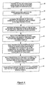
- Figure 4 illustrates a prior art method of placing a die on a target placement area so that the position of the circuit pattern on the top of the die is placed on or over a desired die registration area on the substrate.
- the look down vision system 12 may be placed over a wafer comprising a plurality of dies (not shown) carried on a sticky tape. The sawn wafer permits light from below to shine through the tape at the edges of the die so as to outline a particular die in the wafer which will be acquired and stored in the image processor 18, as shown in block 42.
- the feature of the circuit pattern on the front face of the die surface is illuminated and made visible.
- the circuit pattern and the outer perimeter edges of the die are scanned into the image processor for analysis.
- the process of analysis of the stored information which will be discussed hereinafter proceeds.
- the outer edges of the die's perimeter are extracted in terms of polar coordinates.
- a central value of the edges forming the die's perimeter is calculated as shown at block 47.
- the edges of the die perimeter calculated it is now possible to calculate the outer boundary of the die's circuit pattern and to determine the centroid of the circuit pattern, as shown at block 48.
- another calculation is made including an offset vector for the above centroid.
- a second centroid is calculated for the center of the die perimeter.
- a correction factor is calculated for the die pattern using the extracted centroid's information claimed in steps 46 and 47 and, finally, the correction factor is applied to the mechanical X-Y transport system of the pick and place machine 10, as shown at block 53. It will be observed that the above calculation requires a centroid for the circuit pattern as well as a centroid for an approximate area of the outer perimeter of the die using a calculation of polar coordinates. It will also be observed that the centroid of the outer perimeter of the die component will not be the same as the centroid observed by the aforementioned described horizontal vision system.
- the method shown and described in Figure 4 is explained in greater detail in U.S.-A- 6,031,242.
- the method set forth in Figure 4 was designed for picking die from a sawn or diced wafer, presumably, mounted on a strip of flexible sticky tape such as NittoTM tape.
- the diced wafer is sawn through the wafer but not through the sticky tape, thus leaving a transparent street between die so that the wafer may be back lighted and the streets visually highlighted to a look down vision system 13 of the type employed in prior art vision systems.
- the component 17 to be placed is a surface mount component with highly accurate protruding pins or balls that are indicative of the pattern on the top surface it is possible to use the prior art system shown in Figure 3 accurately to place the component at a desired target or placement location on a substrate or printed circuit board and to ignore the pattern or target on the top of the component.
- the component 17 to be placed does not have such a set of connector pins or balls, it is necessary to determine the location of the desired surface pattern and employ that information to place the component 17 on a substrate 14.
- Figure 5 shows a top or plan view of a substrate or PC board 14 used as part of a fiber optic connector assembly.
- the components 22 to be placed on the substrate 14 must be placed with an accurate spacing of, preferably, 125 or 250 microns, as the case may be.
- the target or feature 54 on the components 22 are typically photo diodes emitters or receivers having a target which is one to two mils in diameter and must be placed within ⁇ twelve microns to assure alignment of the fiber optic cable which is not shown.
- the substrate 14 is provided with highly precise register holes 55 used for mechanical alignment of the connector substrate to be described hereinafter.
- Figure 6 shows a side elevation of a fiber optic connector or assembly including the substrate 14 shown and described in Figure 5.
- the connector assembly of Figure 6 includes an alignment or guide plate 56 which is provided with conical converging apertures 57 which will cause a fiber optic cable to align in precise X-Y position with the target 54 on component 22. It is presumed that the connector assembly is made highly accurate and well within tolerances for deviation so that the placement of a fiber optic cable through the alignment aperture 57 will exactly coincide with the eye point 54 which comprises the center of the active element of the photo diode sensor or receiver. It will be observed that the components 22 placed on the substrate 14 would precisely register the feature 54 on its target position and in alignment with the aperture 57 even if the component 22 has a pattern which is slightly rotated from the outer perimeter of the die. Thus, it is possible to eliminate numerous of the prior art steps and calculations and achieve a more precise placement of the feature 54 than was heretofore possible using a prior art pick and place machine.
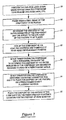
- Figure 7 illustrates a block diagram or flow chart of the preferred embodiment method steps employed accurately to place an active predetermined eye point 54 feature of a component on an exact X, Y location on a substrate 14.
- the blocks or method steps of Figure 7 are to be considered with reference to a prior art pick and place machine shown in Figure 1 having the modification shown in Figure 2.
- the block 58 shows that the look down vision system 12 is placed over the component to be picked up and placed on the substrate 14.
- the vision system does a frame grab or pixel image or pixel map of the component to be placed and stores it in the image processor 18.
- the image processor determines the centroid of the outer perimeter of the component and the offset of the eye point to the feature to be placed.
- the component is picked up by the nozzle 13 as near to the centroid as mechanically accurate and the component 17 is transported to or near the placement position on substrate 14, as shown in block 62.
- a horizontal vision system 24 is employed to determine the centroid of the outer perimeter of the component and also to reduce the rotational position of the component to zero or a predetermined angle. It will be noted that the steps shown in blocks 58 through 63 are steps that have been performed in the prior art systems.
- the eye point 54 of the feature of the component 17 may be placed on an exact X and Y location on the substrate for the eye point disregarding the minor rotation of the pattern, if such exists.
- the exact location of the eye point has been determined within three to five microns using a state of the art horizontal vision system such as the Quad align system shown and described in U.S.-A- 5,559,727.
- Figure 8 shows a block or flow diagram chart of a modified embodiment method employed accurately to place a plurality of active predetermined eye point features on a component onto their exact X and Y placement positions on a substrate 14.
- Block 66 determines the centroid of the outer perimeter of the component and the offset to the main eye point feature which will be employed as explained hereinafter.
- block 67 any rotational error of the pattern on the component relative to the outer perimeter is determined by location of one or two more eye points on the component 17.
- Block 62 is the same as previous block 62 in the Figure 7 and the component is picked up at or near the pick up centroid.
- a horizontal vision system of the type employed in Figure 7 is used to determine the centroid of the outer perimeter of the component and its zero or orthogonal position for placement that would have occurred in block 64 of Figure 7.
- the additional calculation is made of the minor rotational correction for aligning two or more eye points.
- the offset correction in X and Y is made as previously described in block 64 of Figure 7, then subsequently, in block 69, the main eye point feature is placed at the predetermined location for the main eye point on the substrate and the component is rotated in block 68 so that all eye points coincide with predetermined placement position for a plurality of eye points.
- Figure 8 differs from Figure 7 in that only one main eye point has to be placed at a predetermined X-Y target or placement position and that the rotation of the other eye points relative to the main placement eye point is determined so that a rotation correction may be made in block 68 which results in the placement of a plurality of eye points in or on exact target or placement positions.
Landscapes
- Engineering & Computer Science (AREA)
- Manufacturing & Machinery (AREA)
- Microelectronics & Electronic Packaging (AREA)
- Operations Research (AREA)
- Supply And Installment Of Electrical Components (AREA)
- Container, Conveyance, Adherence, Positioning, Of Wafer (AREA)
- Length Measuring Devices By Optical Means (AREA)
- Die Bonding (AREA)
Abstract
Description
Claims (2)
- A method of placing a component on a substrate (14) so that an eye point feature of the component coincides with a predetermined target or placement feature on the substrate, comprising the steps of:sensing the component (17) before pick up with a look down vision system (12),storing a pixel image of the component in a processing means (18),determining the centroid of the outer perimeter of the component (17) to be picked up and the centroid of one or more eye point features to be placed on the substrate (14),picking up the component (17) at or near the centroid of the component and transporting it to or near a placement position,while transporting the component, determining the centroid of the outer perimeter of the component with a horizontal vision system (24)and its orthogonal or zero rotational position, characterised in that the method steps include,while transporting the component, determining any offset correction in the X and Y axes to place a predetermined eye point (54) on a predetermined X and Y placement target position on the substrate (17), andplacing said eye point (54) of the feature of the component on said predetermined location on said substrate.
- A method as claimed in claim 1, wherein said component (17) is placed on said substrate (14) at zero degrees of rotation as seen by the horizontal vision system (24).
Applications Claiming Priority (2)
| Application Number | Priority Date | Filing Date | Title |
|---|---|---|---|
| US59712 | 1987-06-08 | ||
| US10/059,712 US6506614B1 (en) | 2002-01-29 | 2002-01-29 | Method of locating and placing eye point features of a semiconductor die on a substrate |
Publications (3)
| Publication Number | Publication Date |
|---|---|
| EP1331840A2 true EP1331840A2 (en) | 2003-07-30 |
| EP1331840A3 EP1331840A3 (en) | 2005-03-02 |
| EP1331840B1 EP1331840B1 (en) | 2007-03-21 |
Family
ID=22024754
Family Applications (1)
| Application Number | Title | Priority Date | Filing Date |
|---|---|---|---|
| EP03250534A Expired - Lifetime EP1331840B1 (en) | 2002-01-29 | 2003-01-29 | Method of locating and placing eye point features of a semiconductor die on a substrate |
Country Status (9)
| Country | Link |
|---|---|
| US (1) | US6506614B1 (en) |
| EP (1) | EP1331840B1 (en) |
| JP (1) | JP2003264396A (en) |
| KR (1) | KR20030065414A (en) |
| CN (1) | CN1276702C (en) |
| CA (1) | CA2416854A1 (en) |
| DE (1) | DE60312573T2 (en) |
| MX (1) | MXPA03000769A (en) |
| TW (1) | TW200308039A (en) |
Families Citing this family (27)
| Publication number | Priority date | Publication date | Assignee | Title |
|---|---|---|---|---|
| US6504614B1 (en) | 1999-10-08 | 2003-01-07 | Rio Grande Medical Technologies, Inc. | Interferometer spectrometer with reduced alignment sensitivity |
| US7813559B2 (en) * | 2001-11-13 | 2010-10-12 | Cyberoptics Corporation | Image analysis for pick and place machines with in situ component placement inspection |
| US7239399B2 (en) * | 2001-11-13 | 2007-07-03 | Cyberoptics Corporation | Pick and place machine with component placement inspection |
| US7555831B2 (en) * | 2001-11-13 | 2009-07-07 | Cyberoptics Corporation | Method of validating component feeder exchanges |
| US7559134B2 (en) * | 2003-11-04 | 2009-07-14 | Cyberoptics Corporation | Pick and place machine with improved component placement inspection |
| US7706595B2 (en) * | 2003-11-07 | 2010-04-27 | Cyberoptics Corporation | Pick and place machine with workpiece motion inspection |
| US20050125993A1 (en) * | 2003-11-07 | 2005-06-16 | Madsen David D. | Pick and place machine with improved setup and operation procedure |
| US20060016066A1 (en) * | 2004-07-21 | 2006-01-26 | Cyberoptics Corporation | Pick and place machine with improved inspection |
| US20060075631A1 (en) * | 2004-10-05 | 2006-04-13 | Case Steven K | Pick and place machine with improved component pick up inspection |
| US20070003126A1 (en) * | 2005-05-19 | 2007-01-04 | Case Steven K | Method and apparatus for evaluating a component pick action in an electronics assembly machine |
| DE112006002473T5 (en) * | 2005-09-14 | 2008-08-14 | Cyberoptics Corp., Golden Valley | Pick and place machine with improved component pickup image identification processing |
| DE112006003019T5 (en) * | 2005-10-31 | 2008-10-23 | Cyberoptics Corp., Golden Valley | Electronics mounting device with built-in solder paste test |
| US20070276867A1 (en) * | 2006-05-23 | 2007-11-29 | David Fishbaine | Embedded inspection image archival for electronics assembly machines |
| CN103198035B (en) * | 2013-02-28 | 2016-07-20 | 北京优纳科技有限公司 | alignment method and alignment system |
| TWI570823B (en) * | 2013-08-14 | 2017-02-11 | 新川股份有限公司 | Semiconductor manufacturing device and method of manufacturing semiconductor device |
| TWI632626B (en) * | 2016-01-06 | 2018-08-11 | Shinkawa Ltd. | Electronic parts processing unit |
| CN105758309B (en) * | 2016-03-31 | 2018-06-26 | 浙江工业大学 | It is a kind of to utilize the device for rotating single fiber laser arrays guard frame rail position of mounting hole |
| EP3451812B1 (en) * | 2016-04-26 | 2022-11-30 | Fuji Corporation | Substrate work machine |
| US11044841B2 (en) | 2016-09-13 | 2021-06-22 | Universal Instruments Corporation | Feeder system, pick and place machine, and method |
| JP6804741B2 (en) * | 2017-03-23 | 2020-12-23 | 株式会社Fuji | Mounting device and mounting method |
| US10615063B2 (en) * | 2017-11-08 | 2020-04-07 | Facebook Technologies, Llc | Vacuum pick-up head for semiconductor chips |
| CN111102917A (en) * | 2018-10-26 | 2020-05-05 | 得力富企业股份有限公司 | Centroid detection equipment for circuit boards |
| JP6930517B2 (en) * | 2018-12-21 | 2021-09-01 | オムロン株式会社 | Alignment device |
| US12063745B2 (en) * | 2020-05-05 | 2024-08-13 | Integrated Dynamics Engineering Gmbh | Method for processing substrates, in particular wafers, masks or flat panel displays, with a semi-conductor industry machine |
| TWI746320B (en) * | 2020-12-18 | 2021-11-11 | 財團法人工業技術研究院 | Method and system for generating and updating position distribution graph |
| USD1051173S1 (en) | 2023-03-13 | 2024-11-12 | Caterpillar Inc. | Exhaust gas recirculation tube |
| CN116677686B (en) * | 2023-07-31 | 2023-10-20 | 常州铭赛机器人科技股份有限公司 | Mounting method for multiple photographing of chip mounter based on machine vision |
Family Cites Families (12)
| Publication number | Priority date | Publication date | Assignee | Title |
|---|---|---|---|---|
| US3475805A (en) | 1967-06-26 | 1969-11-04 | Ibm | Apparatus for positioning articles on substrates |
| CH643959A5 (en) | 1978-04-14 | 1984-06-29 | Siemens Ag | METHOD AND DEVICE FOR THE AUTOMATIC POSITION DETECTION OF SEMICONDUCTOR CHIPS. |
| US4441205A (en) | 1981-05-18 | 1984-04-03 | Kulicke & Soffa Industries, Inc. | Pattern recognition system |
| EP0075192B1 (en) * | 1981-09-17 | 1990-03-14 | Kabushiki Kaisha Toshiba | An optical head |
| US5189707A (en) | 1985-10-11 | 1993-02-23 | Hitachi, Ltd. | Method of loading surface mounted device and an apparatus therefor |
| US6094268A (en) * | 1989-04-21 | 2000-07-25 | Hitachi, Ltd. | Projection exposure apparatus and projection exposure method |
| US5157734A (en) | 1989-12-19 | 1992-10-20 | Industrial Technology Research Institute | Method and apparatus for picking and placing a surface mounted device with the aid of machine vision |
| US5801432A (en) * | 1992-06-04 | 1998-09-01 | Lsi Logic Corporation | Electronic system using multi-layer tab tape semiconductor device having distinct signal, power and ground planes |
| US5600733A (en) | 1993-11-01 | 1997-02-04 | Kulicke And Soffa Investments, Inc | Method for locating eye points on objects subject to size variations |
| US5559727A (en) | 1994-02-24 | 1996-09-24 | Quad Systems Corporation | Apparatus and method for determining the position of a component prior to placement |
| JPH1154996A (en) * | 1997-07-30 | 1999-02-26 | Tenryu Technic:Kk | Electronic component mounting position correction amount calculation method |
| US6031242A (en) | 1998-01-23 | 2000-02-29 | Zevatech, Inc. | Semiconductor die in-flight registration and orientation method and apparatus |
-
2002
- 2002-01-29 US US10/059,712 patent/US6506614B1/en not_active Expired - Fee Related
-
2003
- 2003-01-21 CA CA002416854A patent/CA2416854A1/en not_active Abandoned
- 2003-01-24 MX MXPA03000769A patent/MXPA03000769A/en unknown
- 2003-01-28 TW TW092101890A patent/TW200308039A/en unknown
- 2003-01-29 KR KR10-2003-0005863A patent/KR20030065414A/en not_active Withdrawn
- 2003-01-29 CN CNB031075576A patent/CN1276702C/en not_active Expired - Fee Related
- 2003-01-29 EP EP03250534A patent/EP1331840B1/en not_active Expired - Lifetime
- 2003-01-29 JP JP2003019596A patent/JP2003264396A/en active Pending
- 2003-01-29 DE DE60312573T patent/DE60312573T2/en not_active Expired - Fee Related
Also Published As
| Publication number | Publication date |
|---|---|
| CN1276702C (en) | 2006-09-20 |
| DE60312573D1 (en) | 2007-05-03 |
| JP2003264396A (en) | 2003-09-19 |
| CN1438836A (en) | 2003-08-27 |
| EP1331840A3 (en) | 2005-03-02 |
| EP1331840B1 (en) | 2007-03-21 |
| KR20030065414A (en) | 2003-08-06 |
| MXPA03000769A (en) | 2004-10-29 |
| US6506614B1 (en) | 2003-01-14 |
| CA2416854A1 (en) | 2003-07-29 |
| DE60312573T2 (en) | 2007-11-29 |
| TW200308039A (en) | 2003-12-16 |
Similar Documents
| Publication | Publication Date | Title |
|---|---|---|
| EP1331840B1 (en) | Method of locating and placing eye point features of a semiconductor die on a substrate | |
| US5768759A (en) | Method and apparatus for reflective in-flight component registration | |
| US6538244B1 (en) | Pick and place machine with improved vision system including a linescan sensor | |
| US5467186A (en) | Attracting nozzle control apparatus for a chip component mounting machine | |
| US4738025A (en) | Automated apparatus and method for positioning multicontact component | |
| US4812666A (en) | Position feedback enhancement over a limited repositioning area for a moveable member | |
| US5547537A (en) | Ceramic carrier transport for die attach equipment | |
| US20100295935A1 (en) | On-head component alignment using multiple area array image detectors | |
| US20090133249A1 (en) | Method and apparatus for evaluating a component pick action in an electronics assembly machine | |
| US4999764A (en) | Method of setting up apparatus for handling electrical or electronic components | |
| EP0920791A2 (en) | Method of placing components on a carrier including a calibration procecure and device suitable threefor | |
| KR20190135422A (en) | Method for calibrating an apparatus for mounting components | |
| EP0829192B1 (en) | Method of placing a component on a substrate and component placement machine for carrying out the method | |
| US6031242A (en) | Semiconductor die in-flight registration and orientation method and apparatus | |
| US6563530B1 (en) | Camera position-correcting method and system and dummy component for use in camera position correction | |
| US5216804A (en) | Method and device for placing a component on a printed circuit board | |
| JP4515814B2 (en) | Mounting accuracy measurement method | |
| JP4562275B2 (en) | Electrical component mounting system and accuracy inspection method thereof | |
| US4893396A (en) | Method of setting up apparatus for handling electrical or electronic components | |
| JP3039645B1 (en) | Electronic component position recognition method and device | |
| JP2001217599A (en) | Surface mount device and electronic component detection method in surface mount device | |
| JPH0761583B2 (en) | How to install chip parts | |
| WO2006125102A1 (en) | Method and apparatus for evaluating a component pick action in an electronics assembly machine | |
| JPH11126995A (en) | Component mounting equipment | |
| CN120784183A (en) | Chip-mounting apparatus and method for mounting a plurality of chips to a carrier plate |
Legal Events
| Date | Code | Title | Description |
|---|---|---|---|
| PUAI | Public reference made under article 153(3) epc to a published international application that has entered the european phase |
Free format text: ORIGINAL CODE: 0009012 |
|
| AK | Designated contracting states |
Designated state(s): AT BE BG CH CY CZ DE DK EE ES FI FR GB GR HU IE IT LI LU MC NL PT SE SI SK TR |
|
| AX | Request for extension of the european patent |
Extension state: AL LT LV MK RO |
|
| PUAL | Search report despatched |
Free format text: ORIGINAL CODE: 0009013 |
|
| AK | Designated contracting states |
Kind code of ref document: A3 Designated state(s): AT BE BG CH CY CZ DE DK EE ES FI FR GB GR HU IE IT LI LU MC NL PT SE SI SK TR |
|
| AX | Request for extension of the european patent |
Extension state: AL LT LV MK RO |
|
| 17P | Request for examination filed |
Effective date: 20050901 |
|
| AKX | Designation fees paid |
Designated state(s): DE ES FR GB IT |
|
| GRAP | Despatch of communication of intention to grant a patent |
Free format text: ORIGINAL CODE: EPIDOSNIGR1 |
|
| GRAS | Grant fee paid |
Free format text: ORIGINAL CODE: EPIDOSNIGR3 |
|
| GRAA | (expected) grant |
Free format text: ORIGINAL CODE: 0009210 |
|
| AK | Designated contracting states |
Kind code of ref document: B1 Designated state(s): DE ES FR GB IT |
|
| REG | Reference to a national code |
Ref country code: GB Ref legal event code: FG4D |
|
| REF | Corresponds to: |
Ref document number: 60312573 Country of ref document: DE Date of ref document: 20070503 Kind code of ref document: P |
|
| PG25 | Lapsed in a contracting state [announced via postgrant information from national office to epo] |
Ref country code: ES Free format text: LAPSE BECAUSE OF FAILURE TO SUBMIT A TRANSLATION OF THE DESCRIPTION OR TO PAY THE FEE WITHIN THE PRESCRIBED TIME-LIMIT Effective date: 20070702 |
|
| EN | Fr: translation not filed | ||
| PLBE | No opposition filed within time limit |
Free format text: ORIGINAL CODE: 0009261 |
|
| STAA | Information on the status of an ep patent application or granted ep patent |
Free format text: STATUS: NO OPPOSITION FILED WITHIN TIME LIMIT |
|
| 26N | No opposition filed |
Effective date: 20071227 |
|
| PG25 | Lapsed in a contracting state [announced via postgrant information from national office to epo] |
Ref country code: FR Free format text: LAPSE BECAUSE OF FAILURE TO SUBMIT A TRANSLATION OF THE DESCRIPTION OR TO PAY THE FEE WITHIN THE PRESCRIBED TIME-LIMIT Effective date: 20071123 Ref country code: IT Free format text: LAPSE BECAUSE OF FAILURE TO SUBMIT A TRANSLATION OF THE DESCRIPTION OR TO PAY THE FEE WITHIN THE PRESCRIBED TIME-LIMIT Effective date: 20070321 |
|
| PGFP | Annual fee paid to national office [announced via postgrant information from national office to epo] |
Ref country code: DE Payment date: 20080229 Year of fee payment: 6 |
|
| GBPC | Gb: european patent ceased through non-payment of renewal fee |
Effective date: 20080129 |
|
| PG25 | Lapsed in a contracting state [announced via postgrant information from national office to epo] |
Ref country code: FR Free format text: LAPSE BECAUSE OF FAILURE TO SUBMIT A TRANSLATION OF THE DESCRIPTION OR TO PAY THE FEE WITHIN THE PRESCRIBED TIME-LIMIT Effective date: 20070321 |
|
| PG25 | Lapsed in a contracting state [announced via postgrant information from national office to epo] |
Ref country code: GB Free format text: LAPSE BECAUSE OF NON-PAYMENT OF DUE FEES Effective date: 20080129 |
|
| PG25 | Lapsed in a contracting state [announced via postgrant information from national office to epo] |
Ref country code: DE Free format text: LAPSE BECAUSE OF NON-PAYMENT OF DUE FEES Effective date: 20090801 |