EP1331657A1 - Method of providing reliable switching for DSL relay array - Google Patents
Method of providing reliable switching for DSL relay array Download PDFInfo
- Publication number
- EP1331657A1 EP1331657A1 EP01440260A EP01440260A EP1331657A1 EP 1331657 A1 EP1331657 A1 EP 1331657A1 EP 01440260 A EP01440260 A EP 01440260A EP 01440260 A EP01440260 A EP 01440260A EP 1331657 A1 EP1331657 A1 EP 1331657A1
- Authority
- EP
- European Patent Office
- Prior art keywords
- current
- row
- column
- relay
- relays
- Prior art date
- Legal status (The legal status is an assumption and is not a legal conclusion. Google has not performed a legal analysis and makes no representation as to the accuracy of the status listed.)
- Granted
Links
- 238000000034 method Methods 0.000 title claims abstract description 9
- 238000004804 winding Methods 0.000 abstract description 8
- 230000004913 activation Effects 0.000 abstract description 4
- 238000003491 array Methods 0.000 abstract description 3
- 230000003213 activating effect Effects 0.000 description 1
- 230000003111 delayed effect Effects 0.000 description 1
- 239000000758 substrate Substances 0.000 description 1
Images


Classifications
-
- H—ELECTRICITY
- H01—ELECTRIC ELEMENTS
- H01H—ELECTRIC SWITCHES; RELAYS; SELECTORS; EMERGENCY PROTECTIVE DEVICES
- H01H67/00—Electrically-operated selector switches
- H01H67/22—Switches without multi-position wipers
- H01H67/24—Co-ordinate-type relay switches having an individual electromagnet at each cross-point
-
- H—ELECTRICITY
- H01—ELECTRIC ELEMENTS
- H01H—ELECTRIC SWITCHES; RELAYS; SELECTORS; EMERGENCY PROTECTIVE DEVICES
- H01H67/00—Electrically-operated selector switches
- H01H67/22—Switches without multi-position wipers
- H01H67/30—Co-ordinate-type selector switches with field of co-ordinate coil acting directly upon magnetic leaf spring or reed-type contact member
Definitions
- This invention relates to an addressing system for arrays of relays. While the invention is suitable for use in miniaturized relays, it can also be used with larger relays.
- the pending unpublished Australian patent application no. 28005/01 discloses a miniaturized relay formed integrally in a substrate such as a printed circuit board.
- the relays are arranged in an array and a row and column addressing system is used to set or reset relays.
- a known method of addressing relays in an array is to provide two windings on each relay, wherein one winding is associated with a row drive signal and one winding is associated with a column drive signal, and half of the required activation current is provided by each winding.
- a known limitation of such addressing arrangements is limited discrimination between selected relays and non-selected relays.
- the present invention relates to an enhanced addressing system for such arrays of relays.
- Discrimination can be increased by providing a current below the minimum trip current in the row coil of the selected relay, and providing twice this current in the column coil of the selected relay.
- an opposite current equal to the first row current, but in the opposite direction is used to counteract the column current and reduce the net magnetic force to below the trip threshold for all relays in those other rows, except for the selected row, where the currents reinforce.
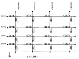
- Figure 1 shows an array of relays with each relay having two activation coils. One coil of each relay is connected to a column drive signal and the remaining coil of each relay is connected to a row drive signal.
- the individual coils in each row or column are connected in series in the figure. Alternatively the individual coils in each row or column could be connected in parallel.
- the row and column drive signals would be typically generated by controllable current or voltage sources.
- the type of control required is polarity of voltage/current and duration. In the case of the use of voltage sources the current is determined by the voltage and total coil resistance of the row or column.
- the individual relays may be made to latch in the activated state after being addressed.
- Example methods of latching include the use of latching type relays which include a bias magnet or the addition of a third coil to each relay which is constantly energized.
- individual relays may be released using a similar addressing system but with the polarity of the applied row and column signals reversed compared to that for setting.
- the row and column coils in figure 1 have one end connected to a driver and one end connected to ground.
- the drivers must be capable of producing three states 1. no current 2. positive current 3. negative current.
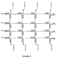
- Figure 2 shows an alternative arrangement where the row and column coils do not have one end grounded, and a differential drive arrangement is used for the row and column coils.
- the row and column drivers can be simplified to have only two states i.e. zero state and positive state.
- Figure 3 shows an example of row and column addressing signals used to apply the invention to a relay array.
- the first two waveforms are the row addressing signals.
- the addressed row has a positive polarity pulse applied while the non-energized rows have negative polarity pulses.
- the second two waveforms are the column addressing signals.
- the addressed column is driven with a positive polarity pulse typically of twice the amplitude of the row pulses.
- the unaddressed columns have no drive applied.
- the relay at the intersection of the addressed row and addressed column is operated by the superposition of the row current and column current.
- the negative row currents in the non-addressed rows serve to increase the ratio of current in the selected relay to current in non-selected relays. This ratio may typically be 3:1 by making the column current twice the row currents. This compares with a ratio of 2:1 for conventional row /column addressing.
- Figure 4 shows an example of the driver waveforms used in a differential drive embodiment of the invention.
- the a drive signals are connected to one end of the row or column coils while the b drive signals are connected to the other end.
- By activating either the a driver or b driver current through the direction of current through the coils may be controlled. With neither driver activated no current flows through the coils.
- the unaddressed rows are driven with waveforms so as to result in a reversed current flow compared to the addressed row.
- the addressed column has a drive signal applied that is typically delayed compared to the row signals to ensure proper addressing.
- Figure 5 shows a row column addressing system for an array of relays using shared row and column coils. Such a system of shared coils is described in the unpublished Australian patent application no. 28005/01.
- the sharing of row and column coils may be achieved by using elongated planar coils that pass through the magnetic aperture of multiple relays comprising a row or column.
- the magnetic aperture of each relay in the array has one elongated row coil and one elongated column coil passing through it.
- the individual relays may be located on top of the row column coil intersection points and be driven by the magnetic field resulting at these points.
- the shared row and column coils may serve one row or column each or may serve two adjacent rows or columns depending on how the coils are passed through the magnetic apertures of the individual relays.
Landscapes
- Physics & Mathematics (AREA)
- Electromagnetism (AREA)
- Control Of Indicators Other Than Cathode Ray Tubes (AREA)
- Relay Circuits (AREA)
- Emergency Protection Circuit Devices (AREA)
- Exchange Systems With Centralized Control (AREA)
Abstract
Description
- This invention relates to an addressing system for arrays of relays. While the invention is suitable for use in miniaturized relays, it can also be used with larger relays.
- The pending unpublished Australian patent application no. 28005/01 discloses a miniaturized relay formed integrally in a substrate such as a printed circuit board. In a preferred embodiment of this arrangement, the relays are arranged in an array and a row and column addressing system is used to set or reset relays.
- A known method of addressing relays in an array is to provide two windings on each relay, wherein one winding is associated with a row drive signal and one winding is associated with a column drive signal, and half of the required activation current is provided by each winding. A known limitation of such addressing arrangements is limited discrimination between selected relays and non-selected relays. The present invention relates to an enhanced addressing system for such arrays of relays.
- The discrimination of row and column addressing in a relay array as discribed above can be improved by the use of "cancelling currents" in the non-addressed relays.
- False operation of relays can occur in a row and column addressing system with insufficient discrimination of activation current between addressed and non-addressed relays.
- Discrimination can be increased by providing a current below the minimum trip current in the row coil of the selected relay, and providing twice this current in the column coil of the selected relay. In all the other rows, an opposite current equal to the first row current, but in the opposite direction is used to counteract the column current and reduce the net magnetic force to below the trip threshold for all relays in those other rows, except for the selected row, where the currents reinforce.
- This gives a 3:1 discrimination between selected and non-selected relays. To prevent false operation, the below the trip threshold currents are applied before the double current is applied to the selected column.
-
- Figure 1 shows a row/column addressing system for an array of relays
- Figure 2 shows a row column addressing system for an array of relays adapted for differential drive
- Figure 3 shows an example of row and column drive signals used to implement the method.
- Figure 4 shows an example of row and column drive signals used to implement a differential drive embodiment of the method
- Figure 5 shows a row/column addressing system for an array of relays using shared/extended coils.
-
- The invention will be described with reference to the accompanying drawings.
Figure 1 shows an array of relays with each relay having two activation coils. One coil of each relay is connected to a column drive signal and the remaining coil of each relay is connected to a row drive signal. The individual coils in each row or column are connected in series in the figure. Alternatively the individual coils in each row or column could be connected in parallel. - The row and column drive signals would be typically generated by controllable current or voltage sources. The type of control required is polarity of voltage/current and duration. In the case of the use of voltage sources the current is determined by the voltage and total coil resistance of the row or column.
- Optionally the individual relays may be made to latch in the activated state after being addressed. Example methods of latching include the use of latching type relays which include a bias magnet or the addition of a third coil to each relay which is constantly energized. In the case of latching operation individual relays may be released using a similar addressing system but with the polarity of the applied row and column signals reversed compared to that for setting.
- The row and column coils in figure 1 have one end connected to a driver and one end connected to ground. In this arrangement the drivers must be capable of producing three
states 1. no current 2.positive current 3. negative current. - Figure 2 shows an alternative arrangement where the row and column coils do not have one end grounded, and a differential drive arrangement is used for the row and column coils. In this arrangement the row and column drivers can be simplified to have only two states i.e. zero state and positive state.
- Figure 3 shows an example of row and column addressing signals used to apply the invention to a relay array.
- The first two waveforms are the row addressing signals. The addressed row has a positive polarity pulse applied while the non-adressed rows have negative polarity pulses.
- The second two waveforms are the column addressing signals. The addressed column is driven with a positive polarity pulse typically of twice the amplitude of the row pulses. The unaddressed columns have no drive applied.
- By delaying the application of the double current column pulse until after the row currents are applied addressing of unselected relays is avoided. Similarly the column drive should be removed before the row drive is removed.
- The relay at the intersection of the addressed row and addressed column is operated by the superposition of the row current and column current. The negative row currents in the non-addressed rows serve to increase the ratio of current in the selected relay to current in non-selected relays. This ratio may typically be 3:1 by making the column current twice the row currents. This compares with a ratio of 2:1 for conventional row /column addressing.
- It shall be understood that the same approach may be applied for an array of arbitary size.
- Figure 4 shows an example of the driver waveforms used in a differential drive embodiment of the invention. The a drive signals are connected to one end of the row or column coils while the b drive signals are connected to the other end. By activating either the a driver or b driver current through the direction of current through the coils may be controlled. With neither driver activated no current flows through the coils.
- The unaddressed rows are driven with waveforms so as to result in a reversed current flow compared to the addressed row.
- The addressed column has a drive signal applied that is typically delayed compared to the row signals to ensure proper addressing.
- In the case of latching relays, resetting of an addressed relay is achieved by reversing the current flow.
- Figure 5 shows a row column addressing system for an array of relays using shared row and column coils. Such a system of shared coils is described in the unpublished Australian patent application no. 28005/01.
- In this arrangement voltages or currents are applied to the shared row and column coils to achieve addressing of selected relays in a manner similar to that described above for separate row and column coils per relay. Since the row and column coils are span the entire row or column there is no need in this case to connect individual relay coils in series or parallel.
- The sharing of row and column coils may be achieved by using elongated planar coils that pass through the magnetic aperture of multiple relays comprising a row or column. In this arrangement the magnetic aperture of each relay in the array has one elongated row coil and one elongated column coil passing through it.
In an alternative embodiment the individual relays may be located on top of the row column coil intersection points and be driven by the magnetic field resulting at these points. - The shared row and column coils may serve one row or column each or may serve two adjacent rows or columns depending on how the coils are passed through the magnetic apertures of the individual relays.
Claims (8)
- A method of operating a relay array using row and column addressing to improve discrimination between selected and non-selected relays, including:wherein the sum of the first and third currents is greater than the trip current.applying a first current less than the trip current to a row containing the selected relay;applying a second current less than the trip current to the other rows, and having the opposite sense to the first current;applying a third current to the column containing the selected relay, the third current having the same sense as the first current;
- A method as claimed in claim 1, wherein the first and second currents have the same value, and wherein the third current has twice the value of the first current.
- A method as claimed in claim 1 or claim 2 in which the second current is applied before the third current.
- A relay array driver having controllable sources to apply a first current to the row containing a selected relay, and to apply a second current of the opposite polarity to the rows which do not contain the selected relay, and to apply a third current to the column which contains the selected relay.
- A relay array driver as claimed in claim 4 wherein the controllable sources are controllable current sources.
- A relay array driver as claimed in claim 4 wherein the controllable sources are controllable voltage sources and the current is then determined by the coil resistances.
- A driver as claimed in claims 4 to 6, including a timer to cause the second current to be applied before the third current.
- A driver as claimed in claims 4 to 7, wherein the rows and columns have drivers at each end and the rows and columns are driven differentially.
Priority Applications (6)
| Application Number | Priority Date | Filing Date | Title |
|---|---|---|---|
| EP01440260A EP1331657B1 (en) | 2001-08-07 | 2001-08-07 | Method of providing reliable switching for DSL relay array |
| DE60100906T DE60100906T2 (en) | 2001-08-07 | 2001-08-07 | Process for the reliable switching of a DSL relay matrix |
| ES01440260T ES2206389T3 (en) | 2001-08-07 | 2001-08-07 | METHOD OF PROVIDING A RELIABLE SWITCH FOR A DSL NETWORK MATRIX. |
| AT01440260T ATE251338T1 (en) | 2001-08-07 | 2001-08-07 | METHOD FOR RELIABLE SWITCHING A DSL RELAY MATRIX |
| US10/201,217 US6741443B2 (en) | 2001-08-07 | 2002-07-24 | Method of providing reliable switching for DSL relay array |
| AU2002300371A AU2002300371B2 (en) | 2001-08-07 | 2002-08-02 | Method of providing reliable switching for DSL relay array |
Applications Claiming Priority (1)
| Application Number | Priority Date | Filing Date | Title |
|---|---|---|---|
| EP01440260A EP1331657B1 (en) | 2001-08-07 | 2001-08-07 | Method of providing reliable switching for DSL relay array |
Publications (2)
| Publication Number | Publication Date |
|---|---|
| EP1331657A1 true EP1331657A1 (en) | 2003-07-30 |
| EP1331657B1 EP1331657B1 (en) | 2003-10-01 |
Family
ID=8183278
Family Applications (1)
| Application Number | Title | Priority Date | Filing Date |
|---|---|---|---|
| EP01440260A Expired - Lifetime EP1331657B1 (en) | 2001-08-07 | 2001-08-07 | Method of providing reliable switching for DSL relay array |
Country Status (6)
| Country | Link |
|---|---|
| US (1) | US6741443B2 (en) |
| EP (1) | EP1331657B1 (en) |
| AT (1) | ATE251338T1 (en) |
| AU (1) | AU2002300371B2 (en) |
| DE (1) | DE60100906T2 (en) |
| ES (1) | ES2206389T3 (en) |
Cited By (1)
| Publication number | Priority date | Publication date | Assignee | Title |
|---|---|---|---|---|
| AU2002300371B2 (en) * | 2001-08-07 | 2007-03-22 | Alcatel | Method of providing reliable switching for DSL relay array |
Families Citing this family (1)
| Publication number | Priority date | Publication date | Assignee | Title |
|---|---|---|---|---|
| CN106653479B (en) * | 2016-11-14 | 2018-11-02 | 合肥同智机电控制技术有限公司 | A kind of multichannel triggering property load triggers control device |
Citations (2)
| Publication number | Priority date | Publication date | Assignee | Title |
|---|---|---|---|---|
| FR77301E (en) * | 1959-09-25 | 1962-02-16 | Int Standard Electric Corp | Switching Device Improvements |
| GB1509822A (en) * | 1975-01-30 | 1978-05-04 | Int Standard Electric Corp | Switching device in which relays are placed in a coordinate arrangement |
Family Cites Families (3)
| Publication number | Priority date | Publication date | Assignee | Title |
|---|---|---|---|---|
| US4868448A (en) * | 1986-09-24 | 1989-09-19 | General Electric Company | Piezoelectric relay switching matrix |
| US6081232A (en) * | 1998-07-06 | 2000-06-27 | The United States Of America As Represented By The Secretary Of The Army | Communication relay and a space-fed phased array radar, both utilizing improved mach-zehnder interferometer |
| EP1331657B1 (en) * | 2001-08-07 | 2003-10-01 | Alcatel | Method of providing reliable switching for DSL relay array |
-
2001
- 2001-08-07 EP EP01440260A patent/EP1331657B1/en not_active Expired - Lifetime
- 2001-08-07 DE DE60100906T patent/DE60100906T2/en not_active Expired - Lifetime
- 2001-08-07 ES ES01440260T patent/ES2206389T3/en not_active Expired - Lifetime
- 2001-08-07 AT AT01440260T patent/ATE251338T1/en not_active IP Right Cessation
-
2002
- 2002-07-24 US US10/201,217 patent/US6741443B2/en not_active Expired - Lifetime
- 2002-08-02 AU AU2002300371A patent/AU2002300371B2/en not_active Ceased
Patent Citations (2)
| Publication number | Priority date | Publication date | Assignee | Title |
|---|---|---|---|---|
| FR77301E (en) * | 1959-09-25 | 1962-02-16 | Int Standard Electric Corp | Switching Device Improvements |
| GB1509822A (en) * | 1975-01-30 | 1978-05-04 | Int Standard Electric Corp | Switching device in which relays are placed in a coordinate arrangement |
Cited By (1)
| Publication number | Priority date | Publication date | Assignee | Title |
|---|---|---|---|---|
| AU2002300371B2 (en) * | 2001-08-07 | 2007-03-22 | Alcatel | Method of providing reliable switching for DSL relay array |
Also Published As
| Publication number | Publication date |
|---|---|
| ATE251338T1 (en) | 2003-10-15 |
| AU2002300371B2 (en) | 2007-03-22 |
| ES2206389T3 (en) | 2004-05-16 |
| DE60100906T2 (en) | 2004-05-19 |
| DE60100906D1 (en) | 2003-11-06 |
| EP1331657B1 (en) | 2003-10-01 |
| US20030030959A1 (en) | 2003-02-13 |
| US6741443B2 (en) | 2004-05-25 |
Similar Documents
| Publication | Publication Date | Title |
|---|---|---|
| DE3919625C2 (en) | Semiconductor memory device | |
| DE69806133T2 (en) | HIGHLY EFFICIENT MAGNETIC INTEGRATED MINIATURE CIRCUIT STRUCTURE | |
| US3990068A (en) | Plasma display panel drive system | |
| DE2246047B2 (en) | Display arrangements | |
| US5157387A (en) | Method and apparatus for activating a liquid crystal display | |
| DE2306067A1 (en) | DEVICE FOR THE QUICK DISPLAY OF VISUAL INFORMATION DEVELOPED BY MAGNETIC DISPLAY ELEMENTS IN THE MOSAIC SYSTEM | |
| JP3909292B2 (en) | Method for writing to magnetoresistive memory cell and porcelain resistive memory written and sold by the method | |
| US4069480A (en) | Blanking circuit for electromagnetic display | |
| WO2006061730A1 (en) | Passive matrix electrophoretic display with reset | |
| EP1331657B1 (en) | Method of providing reliable switching for DSL relay array | |
| US4156872A (en) | Display element write sensor | |
| KR870011481A (en) | Time Division Driving Method of Optical Switch Device Using Ferroelectric Liquid Crystal | |
| DE69018534T2 (en) | Multi-track magnetic head with large field contrast. | |
| US4779082A (en) | Matrix display apparatus employing movable magnetic elements | |
| DE3705488A1 (en) | ELECTROMAGNETIC DISPLAY ELEMENT | |
| US3042905A (en) | Memory systems | |
| US12361267B2 (en) | Operation method of neural network element using spin-orbit torque | |
| KR100450465B1 (en) | Circuit and method for aging acceleration in a mram | |
| US6501686B2 (en) | Electronic driver circuit for word lines in a memory matrix, and memory apparatus | |
| JPH02500936A (en) | Ferroelectric liquid crystal device | |
| DE1285000B (en) | Circuit arrangement for the removal of magnetic storage elements | |
| US3072892A (en) | Magnetic core matrices | |
| DE3335922A1 (en) | Display panel for the visual representation of information | |
| US3500468A (en) | Associative memory devices | |
| DE4302224C2 (en) | Pulse generation circuit for semiconductor device |
Legal Events
| Date | Code | Title | Description |
|---|---|---|---|
| GRAH | Despatch of communication of intention to grant a patent |
Free format text: ORIGINAL CODE: EPIDOS IGRA |
|
| GRAH | Despatch of communication of intention to grant a patent |
Free format text: ORIGINAL CODE: EPIDOS IGRA |
|
| PUAI | Public reference made under article 153(3) epc to a published international application that has entered the european phase |
Free format text: ORIGINAL CODE: 0009012 |
|
| 17P | Request for examination filed |
Effective date: 20020330 |
|
| AK | Designated contracting states |
Designated state(s): AT BE CH CY DE DK ES FI FR GB GR IE IT LI LU MC NL PT SE TR |
|
| AX | Request for extension of the european patent |
Extension state: AL LT LV MK RO SI |
|
| GRAA | (expected) grant |
Free format text: ORIGINAL CODE: 0009210 |
|
| AK | Designated contracting states |
Kind code of ref document: B1 Designated state(s): AT BE CH CY DE DK ES FI FR GB GR IE IT LI LU MC NL PT SE TR |
|
| AX | Request for extension of the european patent |
Extension state: AL LT LV MK RO SI |
|
| PG25 | Lapsed in a contracting state [announced via postgrant information from national office to epo] |
Ref country code: BE Free format text: LAPSE BECAUSE OF FAILURE TO SUBMIT A TRANSLATION OF THE DESCRIPTION OR TO PAY THE FEE WITHIN THE PRESCRIBED TIME-LIMIT Effective date: 20031001 Ref country code: AT Free format text: LAPSE BECAUSE OF FAILURE TO SUBMIT A TRANSLATION OF THE DESCRIPTION OR TO PAY THE FEE WITHIN THE PRESCRIBED TIME-LIMIT Effective date: 20031001 Ref country code: CH Free format text: LAPSE BECAUSE OF FAILURE TO SUBMIT A TRANSLATION OF THE DESCRIPTION OR TO PAY THE FEE WITHIN THE PRESCRIBED TIME-LIMIT Effective date: 20031001 Ref country code: NL Free format text: LAPSE BECAUSE OF FAILURE TO SUBMIT A TRANSLATION OF THE DESCRIPTION OR TO PAY THE FEE WITHIN THE PRESCRIBED TIME-LIMIT Effective date: 20031001 Ref country code: CY Free format text: LAPSE BECAUSE OF FAILURE TO SUBMIT A TRANSLATION OF THE DESCRIPTION OR TO PAY THE FEE WITHIN THE PRESCRIBED TIME-LIMIT Effective date: 20031001 Ref country code: FI Free format text: LAPSE BECAUSE OF FAILURE TO SUBMIT A TRANSLATION OF THE DESCRIPTION OR TO PAY THE FEE WITHIN THE PRESCRIBED TIME-LIMIT Effective date: 20031001 Ref country code: TR Free format text: LAPSE BECAUSE OF FAILURE TO SUBMIT A TRANSLATION OF THE DESCRIPTION OR TO PAY THE FEE WITHIN THE PRESCRIBED TIME-LIMIT Effective date: 20031001 Ref country code: LI Free format text: LAPSE BECAUSE OF FAILURE TO SUBMIT A TRANSLATION OF THE DESCRIPTION OR TO PAY THE FEE WITHIN THE PRESCRIBED TIME-LIMIT Effective date: 20031001 |
|
| REG | Reference to a national code |
Ref country code: GB Ref legal event code: FG4D |
|
| REG | Reference to a national code |
Ref country code: CH Ref legal event code: EP |
|
| REG | Reference to a national code |
Ref country code: IE Ref legal event code: FG4D |
|
| REF | Corresponds to: |
Ref document number: 60100906 Country of ref document: DE Date of ref document: 20031106 Kind code of ref document: P |
|
| PG25 | Lapsed in a contracting state [announced via postgrant information from national office to epo] |
Ref country code: SE Free format text: LAPSE BECAUSE OF FAILURE TO SUBMIT A TRANSLATION OF THE DESCRIPTION OR TO PAY THE FEE WITHIN THE PRESCRIBED TIME-LIMIT Effective date: 20040101 Ref country code: GR Free format text: LAPSE BECAUSE OF FAILURE TO SUBMIT A TRANSLATION OF THE DESCRIPTION OR TO PAY THE FEE WITHIN THE PRESCRIBED TIME-LIMIT Effective date: 20040101 Ref country code: DK Free format text: LAPSE BECAUSE OF FAILURE TO SUBMIT A TRANSLATION OF THE DESCRIPTION OR TO PAY THE FEE WITHIN THE PRESCRIBED TIME-LIMIT Effective date: 20040101 |
|
| NLV1 | Nl: lapsed or annulled due to failure to fulfill the requirements of art. 29p and 29m of the patents act | ||
| LTIE | Lt: invalidation of european patent or patent extension |
Effective date: 20031001 |
|
| REG | Reference to a national code |
Ref country code: CH Ref legal event code: PL |
|
| AKX | Designation fees paid |
Designated state(s): AT BE CH CY DE DK ES FI FR GB GR IE IT LI LU MC NL PT SE TR |
|
| REG | Reference to a national code |
Ref country code: ES Ref legal event code: FG2A Ref document number: 2206389 Country of ref document: ES Kind code of ref document: T3 |
|
| ET | Fr: translation filed | ||
| PLBE | No opposition filed within time limit |
Free format text: ORIGINAL CODE: 0009261 |
|
| STAA | Information on the status of an ep patent application or granted ep patent |
Free format text: STATUS: NO OPPOSITION FILED WITHIN TIME LIMIT |
|
| PG25 | Lapsed in a contracting state [announced via postgrant information from national office to epo] |
Ref country code: LU Free format text: LAPSE BECAUSE OF NON-PAYMENT OF DUE FEES Effective date: 20040807 |
|
| PG25 | Lapsed in a contracting state [announced via postgrant information from national office to epo] |
Ref country code: IE Free format text: LAPSE BECAUSE OF NON-PAYMENT OF DUE FEES Effective date: 20040809 |
|
| PG25 | Lapsed in a contracting state [announced via postgrant information from national office to epo] |
Ref country code: MC Free format text: LAPSE BECAUSE OF NON-PAYMENT OF DUE FEES Effective date: 20040831 |
|
| 26N | No opposition filed |
Effective date: 20040702 |
|
| REG | Reference to a national code |
Ref country code: IE Ref legal event code: MM4A |
|
| PG25 | Lapsed in a contracting state [announced via postgrant information from national office to epo] |
Ref country code: PT Free format text: LAPSE BECAUSE OF NON-PAYMENT OF DUE FEES Effective date: 20040301 |
|
| REG | Reference to a national code |
Ref country code: GB Ref legal event code: 732E Free format text: REGISTERED BETWEEN 20131114 AND 20131120 |
|
| REG | Reference to a national code |
Ref country code: FR Ref legal event code: GC Effective date: 20140717 |
|
| REG | Reference to a national code |
Ref country code: FR Ref legal event code: RG Effective date: 20141016 |
|
| REG | Reference to a national code |
Ref country code: FR Ref legal event code: PLFP Year of fee payment: 15 |
|
| REG | Reference to a national code |
Ref country code: FR Ref legal event code: PLFP Year of fee payment: 16 |
|
| REG | Reference to a national code |
Ref country code: FR Ref legal event code: PLFP Year of fee payment: 17 |
|
| PGFP | Annual fee paid to national office [announced via postgrant information from national office to epo] |
Ref country code: IT Payment date: 20170828 Year of fee payment: 17 Ref country code: ES Payment date: 20170928 Year of fee payment: 17 Ref country code: FR Payment date: 20170822 Year of fee payment: 17 Ref country code: GB Payment date: 20170822 Year of fee payment: 17 |
|
| GBPC | Gb: european patent ceased through non-payment of renewal fee |
Effective date: 20180807 |
|
| REG | Reference to a national code |
Ref country code: GB Ref legal event code: 732E Free format text: REGISTERED BETWEEN 20190429 AND 20190502 |
|
| REG | Reference to a national code |
Ref country code: DE Ref legal event code: R082 Ref document number: 60100906 Country of ref document: DE Representative=s name: MENZIETTI WETZEL, DE Ref country code: DE Ref legal event code: R081 Ref document number: 60100906 Country of ref document: DE Owner name: PROVENANCE ASSET GROUP LLC, PITTSFORD, US Free format text: FORMER OWNER: ALCATEL LUCENT, PARIS, FR |
|
| PG25 | Lapsed in a contracting state [announced via postgrant information from national office to epo] |
Ref country code: IT Free format text: LAPSE BECAUSE OF NON-PAYMENT OF DUE FEES Effective date: 20180807 |
|
| PG25 | Lapsed in a contracting state [announced via postgrant information from national office to epo] |
Ref country code: FR Free format text: LAPSE BECAUSE OF NON-PAYMENT OF DUE FEES Effective date: 20180831 |
|
| REG | Reference to a national code |
Ref country code: ES Ref legal event code: FD2A Effective date: 20190918 |
|
| PG25 | Lapsed in a contracting state [announced via postgrant information from national office to epo] |
Ref country code: ES Free format text: LAPSE BECAUSE OF NON-PAYMENT OF DUE FEES Effective date: 20180808 Ref country code: GB Free format text: LAPSE BECAUSE OF NON-PAYMENT OF DUE FEES Effective date: 20180807 |
|
| PGFP | Annual fee paid to national office [announced via postgrant information from national office to epo] |
Ref country code: DE Payment date: 20200901 Year of fee payment: 20 |
|
| REG | Reference to a national code |
Ref country code: DE Ref legal event code: R071 Ref document number: 60100906 Country of ref document: DE |