EP1331642A1 - Semiconductor storage device, its testing method, and test circuit - Google Patents
Semiconductor storage device, its testing method, and test circuit Download PDFInfo
- Publication number
- EP1331642A1 EP1331642A1 EP01961212A EP01961212A EP1331642A1 EP 1331642 A1 EP1331642 A1 EP 1331642A1 EP 01961212 A EP01961212 A EP 01961212A EP 01961212 A EP01961212 A EP 01961212A EP 1331642 A1 EP1331642 A1 EP 1331642A1
- Authority
- EP
- European Patent Office
- Prior art keywords
- address
- circuit
- test
- refresh
- semiconductor memory
- Prior art date
- Legal status (The legal status is an assumption and is not a legal conclusion. Google has not performed a legal analysis and makes no representation as to the accuracy of the status listed.)
- Withdrawn
Links
- 238000012360 testing method Methods 0.000 title claims abstract description 226
- 239000004065 semiconductor Substances 0.000 title claims abstract description 76
- 238000000034 method Methods 0.000 claims description 38
- 230000008569 process Effects 0.000 claims description 36
- 238000010998 test method Methods 0.000 claims description 23
- 238000013500 data storage Methods 0.000 claims description 11
- 230000008859 change Effects 0.000 claims description 10
- 230000004044 response Effects 0.000 claims description 7
- 230000005856 abnormality Effects 0.000 abstract 1
- 238000004519 manufacturing process Methods 0.000 abstract 1
- 230000007704 transition Effects 0.000 description 9
- 238000010586 diagram Methods 0.000 description 5
- 230000000630 rising effect Effects 0.000 description 4
- 101150110971 CIN7 gene Proteins 0.000 description 3
- 101150110298 INV1 gene Proteins 0.000 description 3
- 101100397044 Xenopus laevis invs-a gene Proteins 0.000 description 3
- 230000007257 malfunction Effects 0.000 description 3
- 230000007547 defect Effects 0.000 description 2
- 230000003111 delayed effect Effects 0.000 description 2
- 230000003213 activating effect Effects 0.000 description 1
- 230000005540 biological transmission Effects 0.000 description 1
- 230000001934 delay Effects 0.000 description 1
- 230000000694 effects Effects 0.000 description 1
- 230000006870 function Effects 0.000 description 1
- 230000005764 inhibitory process Effects 0.000 description 1
- 230000010354 integration Effects 0.000 description 1
- 230000013011 mating Effects 0.000 description 1
- 238000012986 modification Methods 0.000 description 1
- 230000004048 modification Effects 0.000 description 1
- 230000003068 static effect Effects 0.000 description 1
Images


Classifications
-
- G—PHYSICS
- G11—INFORMATION STORAGE
- G11C—STATIC STORES
- G11C29/00—Checking stores for correct operation ; Subsequent repair; Testing stores during standby or offline operation
-
- G—PHYSICS
- G11—INFORMATION STORAGE
- G11C—STATIC STORES
- G11C29/00—Checking stores for correct operation ; Subsequent repair; Testing stores during standby or offline operation
- G11C29/04—Detection or location of defective memory elements, e.g. cell constructio details, timing of test signals
- G11C29/50—Marginal testing, e.g. race, voltage or current testing
- G11C29/50016—Marginal testing, e.g. race, voltage or current testing of retention
-
- G—PHYSICS
- G11—INFORMATION STORAGE
- G11C—STATIC STORES
- G11C29/00—Checking stores for correct operation ; Subsequent repair; Testing stores during standby or offline operation
- G11C29/04—Detection or location of defective memory elements, e.g. cell constructio details, timing of test signals
- G11C29/08—Functional testing, e.g. testing during refresh, power-on self testing [POST] or distributed testing
- G11C29/12—Built-in arrangements for testing, e.g. built-in self testing [BIST] or interconnection details
-
- G—PHYSICS
- G11—INFORMATION STORAGE
- G11C—STATIC STORES
- G11C29/00—Checking stores for correct operation ; Subsequent repair; Testing stores during standby or offline operation
- G11C29/04—Detection or location of defective memory elements, e.g. cell constructio details, timing of test signals
- G11C29/08—Functional testing, e.g. testing during refresh, power-on self testing [POST] or distributed testing
- G11C29/12—Built-in arrangements for testing, e.g. built-in self testing [BIST] or interconnection details
- G11C29/46—Test trigger logic
-
- G—PHYSICS
- G11—INFORMATION STORAGE
- G11C—STATIC STORES
- G11C11/00—Digital stores characterised by the use of particular electric or magnetic storage elements; Storage elements therefor
- G11C11/21—Digital stores characterised by the use of particular electric or magnetic storage elements; Storage elements therefor using electric elements
- G11C11/34—Digital stores characterised by the use of particular electric or magnetic storage elements; Storage elements therefor using electric elements using semiconductor devices
- G11C11/40—Digital stores characterised by the use of particular electric or magnetic storage elements; Storage elements therefor using electric elements using semiconductor devices using transistors
- G11C11/401—Digital stores characterised by the use of particular electric or magnetic storage elements; Storage elements therefor using electric elements using semiconductor devices using transistors forming cells needing refreshing or charge regeneration, i.e. dynamic cells
Definitions
- the present invention relates to a semiconductor memory device, and its test method as well as a test circuit integrated in the semiconductor memory device.
- test circuit For semiconductor memory devices a variety of tests is necessary to make before shipment, for which purpose in many cases, a test circuit has previously been provided in the semiconductor memory device.
- FIG. 1 is a block diagram of a semiconductor memory device with such a test circuit, for example, one structural example of a pseudo SRAM (a pseudo static random access memory).
- the structure of this conventional semiconductor memory device is disclosed in Japanese Laid-open Patent Publication No. 1-125796.
- This semiconductor memory device has the following structure.
- a memory array 1 has a plurality of memory cells which store data.
- a sense amplifier 2 is connected to the memory cell array 1 for amplifying data from the memory array 1.
- a column I/O circuit 3 becomes connected to a bit line of the memory cells in the memory array 1 for selectively activating this bit line.
- a column decoder 4 receives an input of external addresses A8-A15 and is connected to the column I/O circuit 3, so that the external addresses A8-A15 enter into the column I/O circuit 3, whereby the column I/O circuit 3 selectively activates a bit line based on these external addresses A8-A15.
- a main amplifier/write buffer 5 is provided for writing or reading data.
- a multiplexer 8 is connected to an output side of a refresh control circuit 12 and also connected to an output side of an address counter 9, so that in accordance with an output signal from a refresh control circuit 12, the multiplexer 8 selects any of externally entered external addresses A0-A7 and the refresh address outputted from the address counter 9.
- An output side of the multiplexer 8 is connected to a row decoder 7 so that a selected one of the external addresses A0-A7 or the refresh address is inputted into the row decoder 7.
- the row decoder 7 is connected to a word driver 6 so that any one of the external addresses A0-A7 or the refresh address is inputted into the word driver 6.
- the word driver 6 is connected to a word line of the memory cell in the memory array 1, so that the word driver 6 selectively activates the word line based on the external addresses A0-A7 or the refresh address.
- a test mode deciding circuit 10 receives an input of a /CE signal (/ representing a negative logic signal) or a /RFSH signal, so that the test mode deciding circuit 10 decides whether the mode is a test mode or not, and outputs a test signal which indicates the decided result.
- An output control circuit 14 is connected to an output side of the test mode deciding circuit 10, so that the output control circuit 14 is controlled by the test signal outputted from the test mode deciding circuit 1 and outputs an I/O output switching signal.
- the output control circuit 14 is connected to the timer circuit 11 and the I/O output switching circuit 15, so that for test, the output control circuit 14 controls the I/O output switching circuit 15, whereby a frequency divided signal outputted from the timer circuit 11 is supplied through the I/O output switching circuit 15 to an I/O terminal.
- the refresh control circuit 12 receives inputs of the /CE signal and the /RFSH signal, so that if those signals satisfy predetermined conditions, then the refresh control circuit 12 performs refresh operations of the memory cells.
- the above-described timer circuit 11 outputs a refresh request signal periodically at a constant time interval.
- the timer circuit 11 is connected to the refresh control circuit 12 so that the refresh request signal is inputted into the refresh control circuit 12.
- a timing generating circuit 13 is connected to this refresh control circuit 12 for receiving an input of the refresh control signal outputted from the refresh control circuit 12 and also receives external inputs of an /RE signal, an /OE signal and a CS signal, so that the timing generating circuit 13 outputs an internal synchronizing signal and controls operations of the entirety of the circuit.
- the test mode deciding circuit 10 decides that the mode is the test mode.
- the test mode deciding circuit 10 transmits a signal through the output control circuit 14 and outputs this signal for oscillating the timer circuit 11, whereby the refresh control circuit 12 operates the address counter 9 and controls the multiplexer 8, so that the refresh address (n-address) of the address counter 9 is outputted from the multiplexer 8 as the row address of the memory cells.
- the external addresses A8 ⁇ A15 are entered as the column addresses to the column decoder 4.
- a memory cell of a designated address is selected by the row address of n-address and the column addresses A8 ⁇ A15, so that a read out operation of data content of the cell is accomplished. Accordingly, the specific data have previously been written into the cell of this address so that in the test mode, the content in the cell is directly read out, thereby accurately deciding whether or not data have correctly been written and read out. Namely, it is possible to accurately decide whether or not the timer circuit 11 and the address counter 9 normally operate.
- the timer circuit 11 When the mode is set into the test mode, the timer circuit 11 is oscillated, wherein the frequency divided signal outputted from the timer circuit 11 is supplied through the output switching circuit 15 to the I/O7 terminal. Checking the frequency divided output signal results in an accurate decision on whether or the timer circuit 11 normally operates.
- the above described pseudo SRAM is a semiconductor memory device which has the same memory cell structure as the DRAM (dynamic random access memory), and has the same condition in use as the SRAM, wherein it is necessary to internally perform a self-refresh of the memory cells when a predetermined time passes.
- the address of the memory cell to be self-refreshed or the refresh address is generated by the inside of the circuit, for which reason the refresh address is completely irrelevant to the externally supplied read/write addresses.
- the test conducted by the above-described semiconductor memory device is, however, only to check the operation of the timer circuit 11 and also sequentially read out the data of the memory cells by sequentially changing the counted value of the address counter 9. It is impossible to intentionally check the operation or make the test in the worst case which is likely to cause the above-described malfunction.
- an object of the present invention is to provide a semiconductor memory device which is capable of checking operations under any conditions.
- a further object of the present invention is to provide a test circuit integrated in a semiconductor memory device and capable of checking operation under any condition.
- a yet further object of the present invention is to provide a test method capable of checking operation of a semiconductor memory device under any conditions.
- the present invention was made to solve the above issues, and provides a test method for a semiconductor memory device with a plurality of memory cells which need refreshes, wherein during a test operation, there is accomplished, at least one time, a combination of : a read/write process for reading or writing the memory cell based on a first address externally entered ; and a refresh process for refreshing the memory cells based on a second address externally entered.
- the combination of two processes may optionally be that after the refresh process is made, then the read/write process is made.
- the combination of two processes may optionally be that after the read/write process is made, then the refresh process is made.
- the combination of two processes may optionally be made in one cycle.
- the read/write process and subsequent the refresh process and further subsequent the read/write process may optionally be accomplished in one cycle.
- the two processes may optionally be made at a common column address and at row addresses close to each other.
- the two processes may optionally be made at a common column address and at row addresses adjacent to each other.
- the test method for a semiconductor memory device may optionally further include a process of discontinuing the refresh of the memory cell based on a third address generated inside the semiconductor memory device, in response to a switch of the semiconductor memory device from a normal operation mode to a test mode.
- the test address may be selected from the third address and the test address, so that the refresh of the memory cell based on the third address may be discontinued.
- the semiconductor memory device may optionally be switched from the normal operation mode to the test mode based on a mode switching signal externally entered.
- the test address may be selected from the third address and the test address, so that the refresh of the memory cell based on the third address may be discontinued.
- the test operation may optionally be that a set of plural row addresses is subject to the refresh operation with fixing a column address and sequentially changing row addresses.
- the test operation may optionally be that a set of all row addresses is subject to the refresh operation with fixing a column address and sequentially changing row addresses.
- the test operation may optionally be that a set of respective all row addresses for each of plural blocks divided from a memory cell array is subject to the refresh operation with fixing a column address and sequentially changing row addresses.
- Both the first address and the second address may optionally be externally entered every change of the row address.
- the first address may optionally be externally entered every change of the row address, while only an initial address of the second address is externally entered, and the second address may be automatically changed in accordance with a predetermined constant rule every change to the row address.
- a predetermined increment of the second address may optionally be made every change to the row address.
- a hold test of a memory cell to be subject to the test may be previously tested and a predetermined test pattern may be written, before the two processes may be accomplished.
- the present invention provides a semiconductor memory device having a plurality of memory cells which need refresh, a circuit element for supplying a first address, and an access address control circuit for refreshing the memory cell based on an address, wherein the semiconductor memory device further has : a circuit for holding a second address externally entered ; and a refresh address switching circuit electrically coupled to the circuit element for supplying the first address and also coupled to the circuit for holding the second address, and in a normal operation mode, the refresh address switching circuit supplies the first address to the access address control circuit, and in a test mode, the refresh address switching circuit supplies the second address to the access address control circuit.
- the refresh address switching circuit may optionally comprise a selecting circuit which is electrically coupled to the circuit element for supplying the first address and also coupled to the circuit for holding data, and in the normal operation mode, the selecting circuit selects the first address, and in the test mode, the selecting circuit selects the second address.
- the selecting circuit may optionally comprise a multiplexer electrically coupled to the circuit element for supplying the first address and also coupled to the circuit for holding data.
- the semiconductor memory device may optionally further include : a control circuit electrically coupled to the refresh address switching circuit for supplying the refresh address switching circuit a control signal which switches between the normal operation mode and the test mode.
- the control circuit may optionally comprise a test entry circuit which switches between the normal operation mode and the test mode in response to a predetermined external signal.
- the circuit for holding the second address may optionally comprise a data storage device electrically coupled to the refresh address switching circuit.
- the semiconductor memory device may optionally further include an address inverting circuit electrically coupled to between the circuit for holding data and the refresh address switching circuit for inverting the second address outputted from the data storage device, and supplying the same to the refresh address switching circuit.
- the circuit element for supplying the first address may optionally comprise a refresh address generating circuit connected to the refresh address switching circuit.
- the present invention provides a test circuit for a semiconductor memory device, the circuit having a plurality of memory cells which need refresh and a circuit element for supplying a first address based on an internal signal, wherein the test circuit has : a circuit for holding a second address externally entered ; and a refresh address switching circuit electrically coupled to the circuit element for supplying the first address and also coupled to the circuit for holding the second address, and in a normal operation mode, the test circuit supplies the first address to the access address control circuit, and in a test mode, the test circuit supplies the second address to the access address control circuit.
- the refresh address switching circuit may optionally comprise a selecting circuit which is electrically coupled to the circuit element for supplying the first address and also coupled to the circuit for holding data, and in the normal operation mode, the selecting circuit selects the first address, and in the test mode, the selecting circuit selects the second address.
- the selecting circuit may optionally comprise a multiplexer electrically coupled to the circuit element for supplying the first address and also coupled to the circuit for holding data.
- the test circuit may optionally further include : a control circuit electrically coupled to the refresh address switching circuit for supplying the refresh address switching circuit a control signal which switches between the normal operation mode and the test mode.
- the control circuit may optionally comprise a test entry circuit which switches between the normal operation mode and the test mode in response to a predetermined external signal.
- the circuit for holding the second address may optionally comprise a data storage device electrically coupled to the refresh address switching circuit.
- the test circuit may optionally further include an address inverting circuit electrically coupled to between the circuit for holding data and the refresh address switching circuit for inverting the second address outputted from the data storage device, and supplying the same to the refresh address switching circuit.
- the test circuit may optionally be integrated in the semiconductor memory device, or be separated from the semiconductor memory device and be mounted on a same chip as the semiconductor memory device. In either configuration, there is no problem, provided that the test circuit is electrically coupled to the semiconductor memory device, and signals and addresses are transmitted between the test circuit and the semiconductor memory device.
- test circuit is integrated in the semiconductor memory device.
- FIG. 2 is a block diagram showing a circuit configuration of a semiconductor memory device (pseudo SRAM) in accordance with this embodiment.
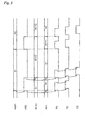
- FIG. 3 is a timing chart of output signals from respective circuits of the semiconductor memory device shown in FIG. 2.
- the circuit configuration of the semiconductor memory device (pseudo SRAM) will be described with reference to FIG. 2, while the output signals from the respective circuits will be described with reference to FIG. 3.
- a read/write address Add is applied to an address terminal 21 from outside.
- a terminal 22 is applied with a first test signal TE1 from outside.
- a terminal 23 is applied with a second test signal TE2 from outside. Only the terminal 22 is a terminal dedicated for the test.
- the terminal 21 is applied with the read/write address Add in the normal operation.
- the terminal 23 is also applied with an output enable signal OE in the normal operation and serves as a terminal for receiving the test signal.
- An address transition detector circuit (ATD circuit) 25 is connected to the terminal 21 for receiving an input of the read/write address Add which was applied to the terminal 21 from outside, so that the address transition detector circuit 25 detects any transition of row address data AddR (see FIG. 3) included in this address data Add. If at least one bit in all bits of the row address data AddR is transitioned, then the address transition detector circuit (ATD circuit) 25 detects the transition and outputs a pulse signal ATD.
- a row control circuit 26 is connected to an output side of the address transition detector circuit (ATD circuit) 25, so that, based on the pulse signal ATD outputted from the address transition detector circuit (ATD circuit) 25, the row control circuit 26 generates and outputs a row enable signal RE, a sense enable signal SE and a column control signal CC.
- the row enable signal RE is a pulse signal which rises at a rising time and a falling time of the pulse signal ATD, and then falls after a predetermined time passes from those times.
- the sense enable signal SE is a signal delayed by a predetermined time from the row enable signal RE.
- the column control signal CC is a later one of two sequential row enable signals RE, namely a signal delayed by a predetermined time from the pulse signal based on the falling of the signal ATD.
- the row control circuit 26 does not output the row enable signal RE.
- a column control circuit 27 is connected to the row control circuit 26 for receiving the column control signal CC outputted from the row control circuit 26 and further delays the column control signal CC, and outputs a column enable signal CE.
- a memory cell array 30 has a similar structure as a memory cell array of DRAM.
- a row decoder 31 is connected to word lines of the memory cell array 30 and also connected to the row control circuit 26, so that at a timing when the row enable signal RE outputted from the row control circuit 26 becomes "1", the row decoder 31 selectively activates a word line of the memory cell array 30, wherein the word line corresponds to row address data RA1 outputted from a multiplexer (MUX) 32.
- MUX multiplexer
- a sense amplifier 33 is connected to each bit line of the memory cell array 30 and also connected to the row control circuit 26, so that the sense amplifier 33 activates each bit line of the memory cell array 30 at a timing when the sense enable signal SE outputted from the row control circuit 26 becomes "1".
- a column decoder 35 is connected to the above-described terminal 21 and the column control circuit 27, so that at a timing when a column enable signal CE outputted from the column control circuit 27 becomes "1", the column decoder 35 decodes column address data AddC included in the address data Add applied to the terminal 21, so that a sense amplifier corresponding to this decode result is connected through an I/O buffer 36 to an input/output data terminal 37.
- a refresh control circuit 40 is a circuit for self-refresh of the memory cell array 30.
- This refresh control circuit 40 is connected to an output side of the address transmission detector circuit (ATD circuit) 25 for receiving the pulse signal ATD and outputs a pulse signal and a reset signal at a time when the pulse signal ATD falls.
- the refresh control circuit 40 is further connected to a timer 42 and a refresh address generating circuit 41, so that the refresh control circuit 40 outputs a pulse signal at a time when the pulse signal ATD falls, and the pulse signal as outputted is entered into the refresh address generating circuit 41, and the reset signal is entered into the timer 42.
- the refresh address generating circuit 41 receives the pulse signal and makes an increment by one of the refresh address RFAD.
- the above-described refresh control circuit 40 detects, based on a timer signal from the timer 40 that any output of the pulse signal ATD from the address transition detector circuit (ATD circuit) does not appear for a predetermined time, so that the refresh control circuit 40 outputs a self-refresh signal RF.
- An output side of the refresh control circuit 40 is connected to the row control circuit 26, so that the self-refresh signal RF as outputted is entered into the row control circuit 26.
- a test circuit 50 for testing a pre-shipment complete product receives inputs of first and second test signals which were applied to the terminals 22 and 23, and the test circuit 50 outputs an output signal T3 and a refresh address RA.
- the refresh control circuit 40 is connected to the test circuit 50 for receiving an input of the output signal T3 and then outputting a signal M and a self-refresh signal RF, whereby a self-refresh of the memory cell array 30 is conducted.
- the test circuit 50 comprises a data store circuit 51, an inverter circuit 52, a test entry circuit 53 and a multiplexer 54.
- the data store circuit 51 captures and outputs row address data AddR included in the address data Add which were applied to the terminal 21, at a timing when the signal T1 outputted from the text entry circuit 53 rises.
- the row address data AddR as outputted is entered into the inverter circuit 52.
- the inverter circuit 52 inverts respective bits outputted from the data store circuit 51 and outputs a test address TA.
- the test entry circuit 53 is connected to the terminals 22 and 23, and the test entry circuit 53 outputs signals T1 ⁇ T3 based on the first and second test signals TE1 and TE2 which were applied to those terminals.
- the multiplexer 54 selects any one of the test address TA from the inverter circuit 52 and the refresh address RFAD from the refresh address generating circuit 41, based on the signal T2 from the test entry circuit 53, and the multiplexer 54 outputs a signal RA.
- This signal RA is entered into the above-described multiplexer 32.
- test mode operation and the normal operation of the above-described semiconductor memory device will be described separately.
- test signal TE1 is set at "0", whereby the signals T1 ⁇ T3 outputted from the test entry circuit 53 become "0".
- the test circuit 50 does not operate, and thus the operation is substantially the same as the semiconductor integrated circuit free of any integration of the test circuit.
- the ATD circuit 25 detects that the data "A1" were applied, whereby the pulse signal ATD ("1") is entered into the row control circuit 26 and the multiplexer 32.
- the multiplexer 32 receives the pulse signal ATD ("1") and outputs data RA from the multiplexer 54 as the row address data RA1.
- the row address data RA1 are then entered into the row decoder 31.
- the multiplexer 54 Since the signal T2 is "0", the multiplexer 54 outputs the refresh address READ which is supplied through the multiplexer 32 to the row decoder 31, provided that the refresh address RFAD was "R1".
- the row control circuit 26 receives the pulse signal ATD and outputs the row enable signal RE.
- This row enable signal RE is entered into the row decoder 31.
- the row decoder 31 receives this row enable signal RE and activates a word line designated by the above-described address data "R1".
- the row control circuit 26 outputs the sense enable signal SE which is then supplied to the sense amplifier 33, whereby the sense amplifier is activated.
- the sense amplifier 33 is activated, a memory cell connected to a word line designated by the above-described row address data "R1" is refreshed.
- the refresh control circuit 40 supplies a pulse signal to the refresh address generating circuit 41, whereby the refresh address RFAD is incremented and becomes "R1+1". Simultaneously, the timer 42 is reset.
- the multiplexer 32 supplies the row decoder 31 the data AddR (data "A1" at this time) as the row address data RA1.
- the row control circuit 26 supplies the row enable signal RE to the row decoder 31.
- the row decoder 31 receives the row enable signal RE and activates a word line of the memory cell array 30, wherein the word line is designated by row address data "A1" outputted from the multiplexer 32. Subsequently, the row control circuit 26 outputs the sense enable signal SE which is then supplied to the sense amplifier 33, whereby a word line corresponding to the address data "A1" of the sense amplifier 33 is activated.
- the column control circuit 27 supplies the column enable signal CE to the column decoder 35.
- the column decoder 35 receives the column enable signal CE and decodes a column address data AddC, so that a sense amplifier corresponding to this decode result is connected through the I/O buffer 36 to the input/output data terminal 37.
- data stored in the memory cell array 30 are transmitted through the sense amplifier 33 and the I/O buffer 36 to the data terminal 37.
- data on the data terminal 37 are written into the memory cell array 30.
- the timer 42 supplies the pulse signal to the refresh control circuit 40.
- the refresh control circuit 40 receives the pulse signal and conducts the self-refresh. Namely, the refresh signal RF is supplied to the row control 26, and the signal M of "1" is supplied to the multiplexer 32.
- the multiplexer 32 receives this signal M and supplies the row decoder 31 the refresh address RFAD (data "R1+1") as the row address data RA1.
- the refresh signal RF is supplied to the row control circuit 26, and then the row control circuit 26 supplies the row enable signal RE to the row decoder 31 and subsequently supplies the sense enable signal SE to the sense amplifier 33, whereby a memory cell connected to a word line corresponding to the row address data "R1+1" is refreshed similarly to the above case.
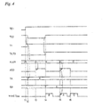
- FIG. 4 is a timing chart for describing the test operation.
- test patterns for the pre-shipment test may be considered.
- a read/write "address B" is "X1”
- "refresh address A” is an inverted address "/X1” of "X1”. The following descriptions will be made by taking one example that the read/write "address B" is "X1” and "refresh address A" is the inverted address "/X1".
- the test signal TE1 rises up to "1", whereby the test entry circuit 53 enters into the test mode, and thereafter the test entry circuit 53 recognizes any signals applied to the terminal 23 to be the second test signal TE2. Subsequently, the address data "X1" are applied to the terminal 21. At a time t2, the second test signal TE2 applied to the terminal 23 falls to "0".
- the second test signal TE2 falls to "0", then the test entry circuit 53 detects this fall, and raises the signal T1 to "1".
- the signal T1 rises to "1", and upon this rising, the data store circuit 51 captures the address data AddR applied to the address terminal 21, namely the address data "X1", whereby the address data "X1" are then supplied to the inverter circuit 52.
- the inverter circuit 52 inverts the address data "X1” and outputs the same as data "/X1".
- the inverted address data "/X1" are supplied as the test address data to the multiplexer 54.
- the inverter 52 is interposed between the data store circuit 51 and the multiplexer 54.
- the multiplexer 32 selects the address "X1" which was entered through the address terminal 21 so that the read or write operation is made at the address "X1".
- the multiplexer 32 selects the inverted address "/X1" which was entered through the address terminal 21 and inverted by the inverter 52, so that the read or write operation is made at the inverted address "/X1".
- the address data "X1" supplied from an external tester may be used commonly for both the read or write operation and the refresh operation. This may make it easy to prepare he test patterns and also make a test program simple.
- the inverter 52 In case the inverter 52 is not provided, it is necessary that the inverted address data "/X1" are applied as the refresh address to the address terminal 21. When the read or write address is changed, then the inverted address as the refresh address is needed to be applied to the address terminal 21. As a result, the test program is likely to be complicated. This is more remarkable as a scale of the memory cell array is large.
- the inverter 52 for allowing the address data applied to the address terminal 21 to be used commonly for both the read or write operation and the refresh operation.
- the inverter 52 is mere circuit design choice and not essential for the test circuit. For example, depending upon the test pattern, it is not necessary that the read or write address B is "X1", the refresh address A is the inverted address "/X1" of "X1". In this case, it is unnecessary to provide, on purpose, the inverter 52.
- the address data "X1 as the read/write address "B” as the address data AddR are applied to the address terminal 21.
- the address data "X1 are applied to the address terminal 21, and as described above, the pulse signal ATD is outputted from the ATD circuit 25.
- the outputted pulse signal ATD is entered into the row control circuit 26. Since at this time, the test signal TE2 is "0", then the row enable signal RE and the sense amplifier enable signal SE are not outputted from the row control circuit 26.
- the second test signal TE2 rises to "1" at a time t4, that a predetermined time (a time slightly longer than a pulse width of the pulse signal ATD) passes from the time t3 when the address data "X1" was applied to the terminal 21.
- the test signal TE2 rises to "1”, and then the test entry circuit 53 detects this rising, and the signals T2 and T3 rise to "1".
- the signal T2 rises to "1", then the multiplexer 54 outputs the test address data TA as the address data RA.
- the signal T3 rises, and the refresh control circuit 40 detects this rising, and supplies the self-refresh signal RF to the row control circuit 26 and also supplies the signal M to the multiplexer 32.
- the signal M is entered into the multiplexer 32, and the multiplexer 32 supplies the address data AddR (the data "X1" at this time) to the row decoder 31.
- the row enable signal RE is outputted from the row control circuit 26.
- This row enable signal RE is then entered into the row decoder 31, whereby a word line designated by the address data "X1" is activated.
- the sense enable signal SE is outputted from the row control circuit 26, the sense amplifier 33 is activated, and the read/write is made to the word line designated by the address data "X1".
- address data "C” are applied to the address terminal 21.
- the ATD circuit 25 detects this, and supplies the pulse signal ATD "1" to the multiplexer 32 and the row control circuit 26.
- the multiplexer 32 selects an output from the multiplexer 54, namely the test address TA (the address data "/X1" as the refresh address A at this time), and then supplies the selected data to the row decoder 31.
- the pulse signal ATD is supplied to the row control circuit 26
- the second test signal TE2 has been "1"
- the row enable signal RE is outputted from the row control circuit 26, and the row enable signal RE as outputted is then entered into the row decoder 31, whereby the word line designated by the address data "/X1" is activated.
- the sense enable signal SE is outputted from the row control circuit 26, and the sense amplifier 33 is activated, whereby the memory cell connected to the word line designated by the address data "/X1" is refreshed.
- the pulse signal ATD falls to "0"
- the multiplexer 32 supplies the address data AddR (data C at this time) to the row decoder 31.
- the row enable signal RE is outputted from the row control circuit 26.
- the row enable signal RE as outputted is entered into the row decoder 31, whereby a word line designated by the address data "C” is activated.
- the sense enable signal SE is outputted from the row control circuit 26, and the sense amplifier 33 is activated, and a read/write operation of the word line designed by the address data "C" is made.
- the test circuit 50 shown in FIG. 2 is capable of previously setting the test-purpose refresh address (the above address data "A") in the data store circuit 51. Since the refresh address "A" previously set in the data storage circuit 51 could have been previously recognized, it is possible that the test-purpose read/write addresses (the above-described address data "B", "C") adjacent to this refresh address are entered from outside, so that the test under any condition, for example, the worst condition, may intentionally and surely made.
- a word line is designated based on the refresh address "A" for refreshing the memory cell and subsequently an adjacent word line to the above word line is designated based on the test-purpose read/write address for the read/write operation, so that the test is intentionally made, wherein adjacent two of the word lines are sequentially activated with fixing a common bit line. Namely, it is possible to verify whether or not any malfunction of the storing operation appears under any conditions, for example, under the worst condition with an insufficient pre-charge or a slight leakage of current under a field insulating film.
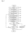
- Step S1 If a chip originally has any stationary defect or has a memory cell with poor hold characteristics, the test for refresh operation makes no sense, for which reason the holding test is needed to be carried out previously (Step S1).
- the holding test may be made in the known test sequences similarly to those of the test taken place for the general-purpose DRAM.
- data are written into memory cells of the memory cell array 30 and the refresh remains inhibited for a predetermined time, before data are read out from the memory cells, wherein the predetermined time (or refresh cycle) is adjusted so that the read out data correspond to the written data, thereby deciding the hold times of the memory cells.
- This test is conducted for all of the memory cells, so that it is possible to decide the refresh cycle based on the shortest hold time of the memory cells.
- the inhibition of the refresh operation may be made by entry of the control signal into the refresh control circuit 40.
- test patterns have previously been written into the memory cell array 30 (Step S2).
- the test pattern with all bits of "1" is used.
- Step S3 An optional hold time is set. Subsequently, the first test signal TE1 is raised to "1" to set the circuit into the test mode (Step S4).
- Address data ("B") are applied to the address terminal 21, wherein the address data ("B") designate a word line which is connected to the same sense amplifier as a word line which is designated by the address data "A” (Step S6).
- Address data are applied to the address terminal 21, wherein the address data ("C") designate a word line which is connected to the same sense amplifier as a word line which is designated by the address data "A” (Step S7).
- Step S8 data stored in the memory cells connected to the respective word lines designated by the above addresses "A", "B” and “C” are read out and then checked (Step S8). If the result of the check is "NG” (Step S9), then the test is finished and the chip is disposed (Step S10). If the result of the check is "PASS” (Step S9), then it is decided whether or not the entirety of the test has been completed (Step S11). If the result of the decision is "NO", then it returns to the step S5.
- a word line is fixed as a refresh word line, while the word lines of the normal accesses before and after the refresh operation are sequentially changed.
- a word line is fixed as a refresh word line, while the word lines of the normal accesses before and after the refresh operation are sequentially changed from the top one to the bottom one.
- the above test process will be repeated by fixing another word line as the refresh word line until all of the word lines have been selected as the refresh word line, whereby the test is made for all of the test patterns.
- the test may be made for all combinations of the row addresses in the each block.
- the test is made by changing the row address, independently of the column addresses.
- the bit line is connected through a column switch to a data bus.
- the data of the memory cells may be influenced depending on how to open the bit lines and pre-charge. Accordingly, it is preferable to conduct the test with further changing the column addresses.
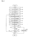
- FIG. 6 is a flow chart of the test to be conducted by changing not only the row addresses but also the column addresses.
- the steps S1 ⁇ S5 are conducted similarly to the above. Thereafter, data "D" as the column address data AddC are applied to the address terminal 21.
- the column decoder 35 decodes the column address data AddC, and a sense amplifier corresponding to the decoded result is connected through the I/O buffer 36 to the input/output data terminal 37. Namely, the bit line is designated by the column address data AddC (Step S12).
- Address data ("B") are applied to the address terminal 21, wherein the address data ("B") designate a word line which is connected to the same sense amplifier as a word line which is designated by the address data "A” (Step S6).
- address data are applied to the address terminal 21, wherein the address data ("C") designate a word line which is connected to the same sense amplifier as a word line which is designated by the address data "A” (Step S7).
- the same test will be repeated by changing the bit lines designated.
- the column address is also changed for the test in order to investigate whether or not the data of the memory cells may be influenced depending on how to open the bit lines and pre-charge.
- enabling to optionally set the address from the outside of the chip increases the flexibility. In other words, designation of all of the addresses should be made from the outside. This is complicated and inconvenience method. It is, however, possible that the above normal access addresses "B" and “C” only are given from the outside, while the refresh address "A" is automatically incremented inside of the circuit, so as to save the programming work for the test program. In this case, it is possible to increment the refresh address by utilizing the address counter in the refresh address generating circuit 41.
- test-purpose refresh address (the above address data "A)
- the increment is made in accordance with the predetermined rule, for which reason it is possible to previously recognize the incremented refresh address (address data "A+1").
- the test-purpose read/write addresses (the above-described address data "B", "C") adjacent to this incremented refresh address are entered from outside, so that the test under any conditions, for example, the worst condition, may intentionally and surely made.
- the word line is designated by the automatically incremented refresh address for taking place the refresh operation of the memory cell, and subsequently the word lines adjacent to the above word line are designated by the test-purpose read/write address for taking place the read/write operation, thereby enabling the test under any optional conditions, for example, the worst condition without designating all of the addresses from the outside.
- the multiplexer 54 receives the refresh address READ outputted from the refresh address generating circuit 41 and also receives the test address TA outputted from the data store circuit 51, and, in the normal operation mode, the multiplexer 54 selects the refresh address RFAD generated in the circuit based on the control signal T2 from the test entry circuit 53, and in the test mode, the multiplexer 54 selects the test address TA entered from the outside.
- the supply of the refresh address RFAD generated inside of the circuit is discontinued, so that in the test mode, it is prevented that the refresh operation is made based on the refresh address RFAD generated inside of the circuit.
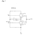
- the multiplexer 54 has a first gate further comprising a first n-type transistor N1 and a first p-type transistor P1, a second gate further comprising a second n-type transistor N2 and a second p-type transistor P2, and an inverter INV1.
- the multiplexer 54 also has a test address input unit for the test address TA which was outputted from the data store circuit 51 and entered through the inverter 52, and a refresh address input unit for receiving an input of the refresh address RFAD outputted from the refresh address generating circuit 41, a control signal input unit for receiving an input of the signal T2 outputted from the test entry circuit 53, and an output unit of the circuit.
- the first gate comprising the first n-type transistor N1 and the first p-type transistor P1 is provided between the test address input unit and the output unit.
- the second gate comprising the second n-type transistor N2 and the second p-type transistor P2 is provided between the refresh address input unit and the output unit.
- control signal input unit is connected to a gate of the first n-type transistor N1, a gate of the second p-type transistor P2, and an input side of the inverter INV1.
- An output side of the inverter INV1 is connected to a gate of the first p-type transistor P1 and a gate of the second n-type transistor N2.
- the signal T2 outputted from the test entry circuit 53 is entered into the gate of the first n-type transistor N1 and the gate of the second p-type transistor P2, while the inverted signal of the signal T2 is entered into the gate of the first p-type transistor P1 and the gate of the second n-type transistor N2.
- the signal T2 is in the inactive state or on low level "L", whereby the first gate comprising the first n-type transistor N1 and the first p-type transistor P1 is closed, while the second gate comprising the second n-type transistor N2 and the second p-type transistor P2 is opened.
- the test address TA is not outputted, while the refresh address RFAD is outputted, so that the refresh operation is made of the memory cell based on the refresh address RFAD generated inside of the circuit in the normal operation mode.
- the signal T2 is in the active state or on high level "H", whereby the first gate comprising the first n-type transistor N1 and the first p-type transistor P1 is opened, while the second gate comprising the second n-type transistor N2 and the second p-type transistor P2 is closed.
- the test address TA is outputted, while the refresh address RFAD is not outputted, so that the refresh operation is made under the worst condition of the memory cell based on the test address TA entered from the outside of the circuit in the test mode.
- the above-multiplexer 54 is only one example of the circuits which have a function of selecting any one of the test address TA and the refresh address RFAD based on the control signal generated upon transition between the normal operation mode and the test mode. It is not unnecessary to limit the circuit to this multiplexer. It is no problem, provided that the row address for access for the read/write operation in the test mode and the row address for access for the refresh operation are surely controllable from the outside.
- test-purpose refresh address (the above address data "A") may previously be set in the data store circuit 51 and the refresh address "A" may previously be recognized, for which reason it is possible that the test-purpose read/write addresses (the above address data "B” and "C") are entered from the outside of the circuit, so that word lines adjacent to the word line designated by the refresh address "A” are designated based on the test-purpose read/write addresses for taking place the test-purpose read/write operations, and subsequently the word line is designated by the refresh address "A” for taking place the refresh operation of the memory cell.
- This allows that the test is intentionally and surely made under the worst conditions, wherein adjacent two of the word lines are sequentially activated with a fixed common bit line.
- one example of the word condition is that the adjacent two of the word lines are sequentially activated with a fixed common bit line. Notwithstanding, this case is not necessarily the worst case. For example, the worst case might be another case that non-adjacent two word lines are sequentially activated with a fixed common bit line. The worst case might be still another case that the bit lines are different and not common. Further, the tests not only under the worst condition but also under other bad conditions might, in case, be needed. In accordance with the present invention, the refresh addresses for the test operation are controllable on the tester side, so that the test operation can surely be made under any conditions.
- test circuit is integrated in the semiconductor memory device. It is possible, if necessary, that the test circuit and the semiconductor memory device are separated from each other but mounted on the same chip. In either structure, there is no problem, provided the test circuit and the semiconductor memory device are electrically coupled to each other for transmitting signals and addresses between the test circuit and the semiconductor memory device.
- the test-purpose refresh address is stored in the internal data storage device, so that the test-purpose addresses corresponding to adjacent word lines to a word line designated by the test-purpose refresh address are applied to the address terminal, whereby the read/write operation is made based on the test-purpose address and subsequently the refresh operation of the memory cell is conducted based on the test-purpose refresh address stored in the data storage device.
- the refresh operation of the memory cell is conducted before the read/write operation is made. Namely, the test may be conducted for any address combination. This allows checking operation in the worst case.
Landscapes
- For Increasing The Reliability Of Semiconductor Memories (AREA)
- Dram (AREA)
- Tests Of Electronic Circuits (AREA)
Abstract
The present invention provides a semiconductor memory device capable of checking operation in the worst case in address combinations, and its manufacturing method. Specific data for test are written into a memory cell array 30. Then, a test signal TE1 is set "1" to set a device in a test mode. Refresh addresses for test are then stored in a data store circuit 51. A first address for test is applied to an address terminal 21, whereby a normal read or write operation is accomplished based on the first address for test. A second address for test is applied to the address terminal 21, whereby a refresh operation is accomplished based on the address for test, and subsequently another normal read or write operation is accomplished based on the second address for test. Data of the memory cell array 30 are checked to decide the presence or absence of any abnormality. <IMAGE>
Description
The present invention relates to a semiconductor memory device,
and its test method as well as a test circuit integrated in the semiconductor
memory device.
For semiconductor memory devices a variety of tests is necessary
to make before shipment, for which purpose in many cases, a test circuit
has previously been provided in the semiconductor memory device.
FIG. 1 is a block diagram of a semiconductor memory device
with such a test circuit, for example, one structural example of a pseudo
SRAM (a pseudo static random access memory). The structure of this
conventional semiconductor memory device is disclosed in Japanese Laid-open
Patent Publication No. 1-125796. This semiconductor memory device
has the following structure.
A memory array 1 has a plurality of memory cells which store
data. A sense amplifier 2 is connected to the memory cell array 1 for
amplifying data from the memory array 1. A column I/O circuit 3 becomes
connected to a bit line of the memory cells in the memory array 1 for
selectively activating this bit line. A column decoder 4 receives an input of
external addresses A8-A15 and is connected to the column I/O circuit 3, so
that the external addresses A8-A15 enter into the column I/O circuit 3,
whereby the column I/O circuit 3 selectively activates a bit line based on
these external addresses A8-A15. Further, a main amplifier/write buffer 5 is
provided for writing or reading data.
A multiplexer 8 is connected to an output side of a refresh control
circuit 12 and also connected to an output side of an address counter 9, so
that in accordance with an output signal from a refresh control circuit 12,
the multiplexer 8 selects any of externally entered external addresses A0-A7
and the refresh address outputted from the address counter 9. An output
side of the multiplexer 8 is connected to a row decoder 7 so that a selected
one of the external addresses A0-A7 or the refresh address is inputted into
the row decoder 7. The row decoder 7 is connected to a word driver 6 so
that any one of the external addresses A0-A7 or the refresh address is
inputted into the word driver 6. The word driver 6 is connected to a word
line of the memory cell in the memory array 1, so that the word driver 6
selectively activates the word line based on the external addresses A0-A7
or the refresh address.
A test mode deciding circuit 10 receives an input of a /CE signal
(/ representing a negative logic signal) or a /RFSH signal, so that the test
mode deciding circuit 10 decides whether the mode is a test mode or not,
and outputs a test signal which indicates the decided result. An output
control circuit 14 is connected to an output side of the test mode deciding
circuit 10, so that the output control circuit 14 is controlled by the test
signal outputted from the test mode deciding circuit 1 and outputs an I/O
output switching signal. Further, the output control circuit 14 is connected
to the timer circuit 11 and the I/O output switching circuit 15, so that for
test, the output control circuit 14 controls the I/O output switching circuit
15, whereby a frequency divided signal outputted from the timer circuit 11
is supplied through the I/O output switching circuit 15 to an I/O terminal.
The refresh control circuit 12 receives inputs of the /CE signal
and the /RFSH signal, so that if those signals satisfy predetermined
conditions, then the refresh control circuit 12 performs refresh operations
of the memory cells. The above-described timer circuit 11 outputs a refresh
request signal periodically at a constant time interval. The timer circuit 11
is connected to the refresh control circuit 12 so that the refresh request
signal is inputted into the refresh control circuit 12. A timing generating
circuit 13 is connected to this refresh control circuit 12 for receiving an
input of the refresh control signal outputted from the refresh control circuit
12 and also receives external inputs of an /RE signal, an /OE signal and a
CS signal, so that the timing generating circuit 13 outputs an internal
synchronizing signal and controls operations of the entirety of the circuit.
In such configurations, if the /RFSH signal is a low level (L) at a
time when the /CE signal transits from a high level (H) to a low level (L),
then the test mode deciding circuit 10 decides that the mode is the test
mode. In this case, the test mode deciding circuit 10 transmits a signal
through the output control circuit 14 and outputs this signal for oscillating
the timer circuit 11, whereby the refresh control circuit 12 operates the
address counter 9 and controls the multiplexer 8, so that the refresh address
(n-address) of the address counter 9 is outputted from the multiplexer 8 as
the row address of the memory cells. The external addresses A8∼A15 are
entered as the column addresses to the column decoder 4.
In the above manners, a memory cell of a designated address is
selected by the row address of n-address and the column addresses A8∼A15,
so that a read out operation of data content of the cell is accomplished.
Accordingly, the specific data have previously been written into the cell of
this address so that in the test mode, the content in the cell is directly read out,
thereby accurately deciding whether or not data have correctly been written
and read out. Namely, it is possible to accurately decide whether or not the
timer circuit 11 and the address counter 9 normally operate.
When the mode is set into the test mode, the timer circuit 11 is
oscillated, wherein the frequency divided signal outputted from the timer
circuit 11 is supplied through the output switching circuit 15 to the I/O7
terminal. Checking the frequency divided output signal results in an
accurate decision on whether or the timer circuit 11 normally operates.
The above described pseudo SRAM is a semiconductor memory
device which has the same memory cell structure as the DRAM (dynamic
random access memory), and has the same condition in use as the SRAM,
wherein it is necessary to internally perform a self-refresh of the memory
cells when a predetermined time passes.
The address of the memory cell to be self-refreshed or the refresh
address is generated by the inside of the circuit, for which reason the
refresh address is completely irrelevant to the externally supplied
read/write addresses.
In the worst case, for example, it is possible that adjacent two of
the word lines are sequentially activated, while the common bit line is
activated. In this case, it is possible that any memory malfunction appears
due to an insufficient pre-charge and a slight leakage of current under a
field insulating film.
The test conducted by the above-described semiconductor
memory device is, however, only to check the operation of the timer circuit
11 and also sequentially read out the data of the memory cells by
sequentially changing the counted value of the address counter 9. It is
impossible to intentionally check the operation or make the test in the worst
case which is likely to cause the above-described malfunction.
In consideration of the above-described circumstances, an object
of the present invention is to provide a semiconductor memory device
which is capable of checking operations under any conditions.
A further object of the present invention is to provide a test
circuit integrated in a semiconductor memory device and capable of
checking operation under any condition.
A yet further object of the present invention is to provide a test
method capable of checking operation of a semiconductor memory device
under any conditions.
The present invention was made to solve the above issues, and
provides a test method for a semiconductor memory device with a plurality
of memory cells which need refreshes, wherein during a test operation,
there is accomplished, at least one time, a combination of : a read/write
process for reading or writing the memory cell based on a first address
externally entered ; and a refresh process for refreshing the memory cells
based on a second address externally entered.
The combination of two processes may optionally be that after
the refresh process is made, then the read/write process is made.
The combination of two processes may optionally be that after
the read/write process is made, then the refresh process is made.
The combination of two processes may optionally be made in
one cycle.
The read/write process and subsequent the refresh process and
further subsequent the read/write process may optionally be accomplished
in one cycle.
The two processes may optionally be made at a common column
address and at row addresses close to each other.
The two processes may optionally be made at a common column
address and at row addresses adjacent to each other.
The test method for a semiconductor memory device may
optionally further include a process of discontinuing the refresh of the
memory cell based on a third address generated inside the semiconductor
memory device, in response to a switch of the semiconductor memory
device from a normal operation mode to a test mode.
When the normal operation mode is switched to the test mode
based on a mode switching signal externally entered, the test address may
be selected from the third address and the test address, so that the refresh of
the memory cell based on the third address may be discontinued.
The semiconductor memory device may optionally be switched
from the normal operation mode to the test mode based on a mode
switching signal externally entered.
When the normal operation mode may be switched to the test
mode based on the mode switching signal externally entered, the test
address may be selected from the third address and the test address, so that
the refresh of the memory cell based on the third address may be
discontinued.
The test operation may optionally be that a set of plural row
addresses is subject to the refresh operation with fixing a column address
and sequentially changing row addresses.
The test operation may optionally be that a set of all row
addresses is subject to the refresh operation with fixing a column address
and sequentially changing row addresses.
The test operation may optionally be that a set of respective all
row addresses for each of plural blocks divided from a memory cell array is
subject to the refresh operation with fixing a column address and
sequentially changing row addresses.
Both the first address and the second address may optionally be
externally entered every change of the row address.
The first address may optionally be externally entered every
change of the row address, while only an initial address of the second
address is externally entered, and the second address may be automatically
changed in accordance with a predetermined constant rule every change to
the row address.
A predetermined increment of the second address may optionally
be made every change to the row address.
A hold test of a memory cell to be subject to the test may be
previously tested and a predetermined test pattern may be written, before
the two processes may be accomplished.
The present invention provides a semiconductor memory device
having a plurality of memory cells which need refresh, a circuit element for
supplying a first address, and an access address control circuit for
refreshing the memory cell based on an address, wherein the semiconductor
memory device further has : a circuit for holding a second address
externally entered ; and a refresh address switching circuit electrically
coupled to the circuit element for supplying the first address and also
coupled to the circuit for holding the second address, and in a normal
operation mode, the refresh address switching circuit supplies the first
address to the access address control circuit, and in a test mode, the refresh
address switching circuit supplies the second address to the access address
control circuit.
The refresh address switching circuit may optionally comprise a
selecting circuit which is electrically coupled to the circuit element for
supplying the first address and also coupled to the circuit for holding data,
and in the normal operation mode, the selecting circuit selects the first
address, and in the test mode, the selecting circuit selects the second
address.
The selecting circuit may optionally comprise a multiplexer
electrically coupled to the circuit element for supplying the first address
and also coupled to the circuit for holding data.
The semiconductor memory device may optionally further
include : a control circuit electrically coupled to the refresh address
switching circuit for supplying the refresh address switching circuit a
control signal which switches between the normal operation mode and the
test mode.
The control circuit may optionally comprise a test entry circuit
which switches between the normal operation mode and the test mode in
response to a predetermined external signal.
The circuit for holding the second address may optionally
comprise a data storage device electrically coupled to the refresh address
switching circuit.
The semiconductor memory device may optionally further
include an address inverting circuit electrically coupled to between the
circuit for holding data and the refresh address switching circuit for
inverting the second address outputted from the data storage device, and
supplying the same to the refresh address switching circuit.
The circuit element for supplying the first address may optionally
comprise a refresh address generating circuit connected to the refresh
address switching circuit.
The present invention provides a test circuit for a semiconductor
memory device, the circuit having a plurality of memory cells which need
refresh and a circuit element for supplying a first address based on an
internal signal, wherein the test circuit has : a circuit for holding a second
address externally entered ; and a refresh address switching circuit
electrically coupled to the circuit element for supplying the first address
and also coupled to the circuit for holding the second address, and in a
normal operation mode, the test circuit supplies the first address to the
access address control circuit, and in a test mode, the test circuit supplies
the second address to the access address control circuit.
The refresh address switching circuit may optionally comprise a
selecting circuit which is electrically coupled to the circuit element for
supplying the first address and also coupled to the circuit for holding data,
and in the normal operation mode, the selecting circuit selects the first
address, and in the test mode, the selecting circuit selects the second
address.
The selecting circuit may optionally comprise a multiplexer
electrically coupled to the circuit element for supplying the first address
and also coupled to the circuit for holding data.
The test circuit may optionally further include : a control circuit
electrically coupled to the refresh address switching circuit for supplying
the refresh address switching circuit a control signal which switches
between the normal operation mode and the test mode.
The control circuit may optionally comprise a test entry circuit
which switches between the normal operation mode and the test mode in
response to a predetermined external signal.
The circuit for holding the second address may optionally
comprise a data storage device electrically coupled to the refresh address
switching circuit.
The test circuit may optionally further include an address
inverting circuit electrically coupled to between the circuit for holding data
and the refresh address switching circuit for inverting the second address
outputted from the data storage device, and supplying the same to the
refresh address switching circuit.
The test circuit may optionally be integrated in the
semiconductor memory device, or be separated from the semiconductor
memory device and be mounted on a same chip as the semiconductor
memory device. In either configuration, there is no problem, provided that
the test circuit is electrically coupled to the semiconductor memory device,
and signals and addresses are transmitted between the test circuit and the
semiconductor memory device.
One embodiment of the present invention will, hereinafter, be
described with reference to the drawings. In the following embodiment,
one structural example is shown, wherein the test circuit is integrated in the
semiconductor memory device.
FIG. 2 is a block diagram showing a circuit configuration of a
semiconductor memory device (pseudo SRAM) in accordance with this
embodiment. FIG. 3 is a timing chart of output signals from respective
circuits of the semiconductor memory device shown in FIG. 2. The circuit
configuration of the semiconductor memory device (pseudo SRAM) will be
described with reference to FIG. 2, while the output signals from the
respective circuits will be described with reference to FIG. 3. A read/write
address Add is applied to an address terminal 21 from outside. A terminal
22 is applied with a first test signal TE1 from outside. A terminal 23 is
applied with a second test signal TE2 from outside. Only the terminal 22 is
a terminal dedicated for the test. The terminal 21 is applied with the
read/write address Add in the normal operation. The terminal 23 is also
applied with an output enable signal OE in the normal operation and serves
as a terminal for receiving the test signal.
An address transition detector circuit (ATD circuit) 25 is
connected to the terminal 21 for receiving an input of the read/write
address Add which was applied to the terminal 21 from outside, so that the
address transition detector circuit 25 detects any transition of row address
data AddR (see FIG. 3) included in this address data Add. If at least one bit
in all bits of the row address data AddR is transitioned, then the address
transition detector circuit (ATD circuit) 25 detects the transition and
outputs a pulse signal ATD.
A row control circuit 26 is connected to an output side of the
address transition detector circuit (ATD circuit) 25, so that, based on the
pulse signal ATD outputted from the address transition detector circuit
(ATD circuit) 25, the row control circuit 26 generates and outputs a row
enable signal RE, a sense enable signal SE and a column control signal CC.
As shown in FIG. 3, the row enable signal RE is a pulse signal which rises
at a rising time and a falling time of the pulse signal ATD, and then falls
after a predetermined time passes from those times. The sense enable signal
SE is a signal delayed by a predetermined time from the row enable signal
RE. Even not shown in the drawing, the column control signal CC is a later
one of two sequential row enable signals RE, namely a signal delayed by a
predetermined time from the pulse signal based on the falling of the signal
ATD. When the second text TE2 is "0" or in the low level, the row control
circuit 26 does not output the row enable signal RE.
A column control circuit 27 is connected to the row control
circuit 26 for receiving the column control signal CC outputted from the
row control circuit 26 and further delays the column control signal CC, and
outputs a column enable signal CE.
A memory cell array 30 has a similar structure as a memory cell
array of DRAM. A row decoder 31 is connected to word lines of the
memory cell array 30 and also connected to the row control circuit 26, so
that at a timing when the row enable signal RE outputted from the row
control circuit 26 becomes "1", the row decoder 31 selectively activates a
word line of the memory cell array 30, wherein the word line corresponds
to row address data RA1 outputted from a multiplexer (MUX) 32.
A sense amplifier 33 is connected to each bit line of the memory
cell array 30 and also connected to the row control circuit 26, so that the
sense amplifier 33 activates each bit line of the memory cell array 30 at a
timing when the sense enable signal SE outputted from the row control
circuit 26 becomes "1".
A column decoder 35 is connected to the above-described
terminal 21 and the column control circuit 27, so that at a timing when a
column enable signal CE outputted from the column control circuit 27
becomes "1", the column decoder 35 decodes column address data AddC
included in the address data Add applied to the terminal 21, so that a sense
amplifier corresponding to this decode result is connected through an I/O
buffer 36 to an input/output data terminal 37.
A refresh control circuit 40 is a circuit for self-refresh of the
memory cell array 30. This refresh control circuit 40 is connected to an
output side of the address transmission detector circuit (ATD circuit) 25 for
receiving the pulse signal ATD and outputs a pulse signal and a reset signal
at a time when the pulse signal ATD falls. The refresh control circuit 40 is
further connected to a timer 42 and a refresh address generating circuit 41,
so that the refresh control circuit 40 outputs a pulse signal at a time when
the pulse signal ATD falls, and the pulse signal as outputted is entered into
the refresh address generating circuit 41, and the reset signal is entered into
the timer 42. The refresh address generating circuit 41 receives the pulse
signal and makes an increment by one of the refresh address RFAD.
The above-described refresh control circuit 40 detects, based on a
timer signal from the timer 40 that any output of the pulse signal ATD from
the address transition detector circuit (ATD circuit) does not appear for a
predetermined time, so that the refresh control circuit 40 outputs a self-refresh
signal RF. An output side of the refresh control circuit 40 is
connected to the row control circuit 26, so that the self-refresh signal RF as
outputted is entered into the row control circuit 26.
Further, a test circuit 50 for testing a pre-shipment complete
product receives inputs of first and second test signals which were applied
to the terminals 22 and 23, and the test circuit 50 outputs an output signal
T3 and a refresh address RA. The refresh control circuit 40 is connected to
the test circuit 50 for receiving an input of the output signal T3 and then
outputting a signal M and a self-refresh signal RF, whereby a self-refresh of
the memory cell array 30 is conducted.
The test circuit 50 comprises a data store circuit 51, an inverter
circuit 52, a test entry circuit 53 and a multiplexer 54. The data store circuit
51 captures and outputs row address data AddR included in the address
data Add which were applied to the terminal 21, at a timing when the signal
T1 outputted from the text entry circuit 53 rises. The row address data
AddR as outputted is entered into the inverter circuit 52. The inverter
circuit 52 inverts respective bits outputted from the data store circuit 51 and
outputs a test address TA. The test entry circuit 53 is connected to the
terminals 22 and 23, and the test entry circuit 53 outputs signals T1 ∼ T3
based on the first and second test signals TE1 and TE2 which were applied
to those terminals. The multiplexer 54 selects any one of the test address
TA from the inverter circuit 52 and the refresh address RFAD from the
refresh address generating circuit 41, based on the signal T2 from the test
entry circuit 53, and the multiplexer 54 outputs a signal RA. This signal RA
is entered into the above-described multiplexer 32.
The test mode operation and the normal operation of the above-described
semiconductor memory device will be described separately.
Initially, the normal operation will be described with reference to
FIG. 3. In this mode, the test signal TE1 is set at "0", whereby the signals
T1 ∼ T3 outputted from the test entry circuit 53 become "0". In the normal
operation, the test circuit 50 does not operate, and thus the operation is
substantially the same as the semiconductor integrated circuit free of any
integration of the test circuit.
In this state, when data "A1" as the row address data AddR are
applied to the terminal 21, the ATD circuit 25 detects that the data "A1"
were applied, whereby the pulse signal ATD ("1") is entered into the row
control circuit 26 and the multiplexer 32. The multiplexer 32 receives the
pulse signal ATD ("1") and outputs data RA from the multiplexer 54 as the
row address data RA1. The row address data RA1 are then entered into the
row decoder 31.
Since the signal T2 is "0", the multiplexer 54 outputs the refresh
address READ which is supplied through the multiplexer 32 to the row
decoder 31, provided that the refresh address RFAD was "R1".
On the other hand, the row control circuit 26 receives the pulse
signal ATD and outputs the row enable signal RE. This row enable signal
RE is entered into the row decoder 31. The row decoder 31 receives this
row enable signal RE and activates a word line designated by the above-described
address data "R1".
Subsequently, the row control circuit 26 outputs the sense enable
signal SE which is then supplied to the sense amplifier 33, whereby the
sense amplifier is activated. After the sense amplifier 33 is activated, a
memory cell connected to a word line designated by the above-described
row address data "R1" is refreshed.
When the pulse signal ATD falls, the refresh control circuit 40
supplies a pulse signal to the refresh address generating circuit 41, whereby
the refresh address RFAD is incremented and becomes "R1+1".
Simultaneously, the timer 42 is reset. When the pulse signal ATD falls, the
multiplexer 32 supplies the row decoder 31 the data AddR (data "A1" at
this time) as the row address data RA1. When the pulse signal ATD falls,
the row control circuit 26 supplies the row enable signal RE to the row
decoder 31.
The row decoder 31 receives the row enable signal RE and
activates a word line of the memory cell array 30, wherein the word line is
designated by row address data "A1" outputted from the multiplexer 32.
Subsequently, the row control circuit 26 outputs the sense enable signal SE
which is then supplied to the sense amplifier 33, whereby a word line
corresponding to the address data "A1" of the sense amplifier 33 is
activated.
Subsequently, the column control circuit 27 supplies the column
enable signal CE to the column decoder 35. The column decoder 35
receives the column enable signal CE and decodes a column address data
AddC, so that a sense amplifier corresponding to this decode result is
connected through the I/O buffer 36 to the input/output data terminal 37. In
case of read operation, data stored in the memory cell array 30 are
transmitted through the sense amplifier 33 and the I/O buffer 36 to the data
terminal 37. In case of write operation, data on the data terminal 37 are
written into the memory cell array 30.
As described above, in accordance with the semiconductor
memory device of FIG. 2, after the read/write address data Add are applied
to the address terminal 21, a refresh of a memory cell connected to a word
line designated by the refresh address RFAD is made and subsequently a
read/write operation of the memory cell array 30 is made based on the
address data Add.
If the read/write operation of the memory cell array 30 has not
been conducted within a predetermined time period, then the timer 42
supplies the pulse signal to the refresh control circuit 40. The refresh
control circuit 40 receives the pulse signal and conducts the self-refresh.
Namely, the refresh signal RF is supplied to the row control 26, and the
signal M of "1" is supplied to the multiplexer 32. The multiplexer 32
receives this signal M and supplies the row decoder 31 the refresh address
RFAD (data "R1+1") as the row address data RA1.
The refresh signal RF is supplied to the row control circuit 26,
and then the row control circuit 26 supplies the row enable signal RE to the
row decoder 31 and subsequently supplies the sense enable signal SE to the
sense amplifier 33, whereby a memory cell connected to a word line
corresponding to the row address data "R1+1" is refreshed similarly to the
above case.
The above describes the normal operation of the semiconductor
memory device shown in FIG. 2.
Subsequently, the pre-shipment test operation using the test
circuit 50 will be described with reference to FIG. 4, which is a timing chart
for describing the test operation.
A variety of patterns as test patterns for the pre-shipment test
may be considered. As one example, it is possible to conduct the test,
wherein a read/write "address B" is "X1", and "refresh address A" is an
inverted address "/X1" of "X1". The following descriptions will be made
by taking one example that the read/write "address B" is "X1" and "refresh
address A" is the inverted address "/X1".
In this pre-shipment test, at a time t1, the test signal TE1 rises up
to "1", whereby the test entry circuit 53 enters into the test mode, and
thereafter the test entry circuit 53 recognizes any signals applied to the
terminal 23 to be the second test signal TE2. Subsequently, the address data
"X1" are applied to the terminal 21. At a time t2, the second test signal TE2
applied to the terminal 23 falls to "0".
The second test signal TE2 falls to "0", then the test entry circuit
53 detects this fall, and raises the signal T1 to "1". The signal T1 rises to
"1", and upon this rising, the data store circuit 51 captures the address data
AddR applied to the address terminal 21, namely the address data "X1",
whereby the address data "X1" are then supplied to the inverter circuit 52.
The inverter circuit 52 inverts the address data "X1" and outputs the same
as data "/X1". The inverted address data "/X1" are supplied as the test
address data to the multiplexer 54.
In the above embodiment, as described above, the inverter 52 is
interposed between the data store circuit 51 and the multiplexer 54. Thus, it
is possible to conduct the refresh at the inverted address "/X1" and the
read/write operation at the address "X1" without any change to the address
data "X1" to be applied to the address terminal 21. Namely, in the read or
write operation, the multiplexer 32 selects the address "X1" which was
entered through the address terminal 21 so that the read or write operation
is made at the address "X1". In the refresh operation, the multiplexer 32
selects the inverted address "/X1" which was entered through the address
terminal 21 and inverted by the inverter 52, so that the read or write
operation is made at the inverted address "/X1".
The address data "X1" supplied from an external tester may be
used commonly for both the read or write operation and the refresh
operation. This may make it easy to prepare he test patterns and also make
a test program simple.
In case the inverter 52 is not provided, it is necessary that the
inverted address data "/X1" are applied as the refresh address to the address
terminal 21. When the read or write address is changed, then the inverted
address as the refresh address is needed to be applied to the address
terminal 21. As a result, the test program is likely to be complicated. This is
more remarkable as a scale of the memory cell array is large.
Accordingly, it is preferable to provide the inverter 52 for
allowing the address data applied to the address terminal 21 to be used
commonly for both the read or write operation and the refresh operation.
The inverter 52 is mere circuit design choice and not essential for the test
circuit. For example, depending upon the test pattern, it is not necessary
that the read or write address B is "X1", the refresh address A is the
inverted address "/X1" of "X1". In this case, it is unnecessary to provide,
on purpose, the inverter 52.
At a time t3, the address data "X1 as the read/write address "B"
as the address data AddR are applied to the address terminal 21. The
address data "X1 are applied to the address terminal 21, and as described
above, the pulse signal ATD is outputted from the ATD circuit 25. The
outputted pulse signal ATD is entered into the row control circuit 26. Since
at this time, the test signal TE2 is "0", then the row enable signal RE and
the sense amplifier enable signal SE are not outputted from the row control
circuit 26.
The second test signal TE2 rises to "1" at a time t4, that a
predetermined time (a time slightly longer than a pulse width of the pulse
signal ATD) passes from the time t3 when the address data "X1" was
applied to the terminal 21. The test signal TE2 rises to "1", and then the test
entry circuit 53 detects this rising, and the signals T2 and T3 rise to "1".
The signal T2 rises to "1", then the multiplexer 54 outputs the test address
data TA as the address data RA.
At this time t4, the signal T3 rises, and the refresh control circuit
40 detects this rising, and supplies the self-refresh signal RF to the row
control circuit 26 and also supplies the signal M to the multiplexer 32. The
signal M is entered into the multiplexer 32, and the multiplexer 32 supplies
the address data AddR (the data "X1" at this time) to the row decoder 31.
When the signal RF is entered into the row control circuit 26, the second
test signal TE2 has already risen to "1". Thus, the row enable signal RE is
outputted from the row control circuit 26. This row enable signal RE is
then entered into the row decoder 31, whereby a word line designated by
the address data "X1" is activated. Subsequently, the sense enable signal SE
is outputted from the row control circuit 26, the sense amplifier 33 is
activated, and the read/write is made to the word line designated by the
address data "X1".
At a time t5, address data "C" are applied to the address terminal
21. When the address data "C" are applied to the address terminal 21, then
the ATD circuit 25 detects this, and supplies the pulse signal ATD "1" to
the multiplexer 32 and the row control circuit 26. The multiplexer 32
selects an output from the multiplexer 54, namely the test address TA (the
address data "/X1" as the refresh address A at this time), and then supplies
the selected data to the row decoder 31. As the pulse signal ATD is
supplied to the row control circuit 26, the second test signal TE2 has been
"1", and thus the row enable signal RE is outputted from the row control
circuit 26, and the row enable signal RE as outputted is then entered into
the row decoder 31, whereby the word line designated by the address data
"/X1" is activated. Subsequently, the sense enable signal SE is outputted
from the row control circuit 26, and the sense amplifier 33 is activated,
whereby the memory cell connected to the word line designated by the
address data "/X1" is refreshed.
At a time t6, the pulse signal ATD falls to "0", then the
multiplexer 32 supplies the address data AddR (data C at this time) to the
row decoder 31. When the pulse signal ATD falls to "0", the row enable
signal RE is outputted from the row control circuit 26. The row enable
signal RE as outputted is entered into the row decoder 31, whereby a word
line designated by the address data "C" is activated. Subsequently, the
sense enable signal SE is outputted from the row control circuit 26, and the
sense amplifier 33 is activated, and a read/write operation of the word line
designed by the address data "C" is made.
As described above, the test circuit 50 shown in FIG. 2 is capable
of previously setting the test-purpose refresh address (the above address
data "A") in the data store circuit 51. Since the refresh address "A"
previously set in the data storage circuit 51 could have been previously
recognized, it is possible that the test-purpose read/write addresses (the
above-described address data "B", "C") adjacent to this refresh address are
entered from outside, so that the test under any condition, for example, the
worst condition, may intentionally and surely made.
A word line is designated based on the refresh address "A" for
refreshing the memory cell and subsequently an adjacent word line to the
above word line is designated based on the test-purpose read/write address
for the read/write operation, so that the test is intentionally made, wherein
adjacent two of the word lines are sequentially activated with fixing a
common bit line. Namely, it is possible to verify whether or not any
malfunction of the storing operation appears under any conditions, for
example, under the worst condition with an insufficient pre-charge or a
slight leakage of current under a field insulating film.
The pre-shipment test using the above-described test circuit 50
will be described with reference to the flow chart of FIG. 5.
If a chip originally has any stationary defect or has a memory cell
with poor hold characteristics, the test for refresh operation makes no
sense, for which reason the holding test is needed to be carried out
previously (Step S1). The holding test may be made in the known test
sequences similarly to those of the test taken place for the general-purpose
DRAM.
Namely, data are written into memory cells of the memory cell
array 30 and the refresh remains inhibited for a predetermined time, before
data are read out from the memory cells, wherein the predetermined time
(or refresh cycle) is adjusted so that the read out data correspond to the
written data, thereby deciding the hold times of the memory cells. This test
is conducted for all of the memory cells, so that it is possible to decide the
refresh cycle based on the shortest hold time of the memory cells. The
inhibition of the refresh operation may be made by entry of the control
signal into the refresh control circuit 40.
Subsequently, in order to make a post-test decision on whether or
not the refresh operation and the read/write operation are made correctly,
the test patterns have previously been written into the memory cell array 30
(Step S2). In order to investigate the normality of the refresh operation and
the read/write operation, the test pattern with all bits of "1" is used.
An optional hold time is set (Step S3). Subsequently, the first test
signal TE1 is raised to "1" to set the circuit into the test mode (Step S4).
Subsequently, the refresh address data ("A") are applied to the
address terminal 21, to cause the test signal TE2 to fall to "0", whereby
the address data "A" are written into the data store circuit 51 (Step
S5).
Address data ("B") are applied to the address terminal 21,
wherein the address data ("B") designate a word line which is connected to
the same sense amplifier as a word line which is designated by the address
data "A" (Step S6).
After the predetermined time has passed, similarly to the above,
Address data ("C") are applied to the address terminal 21, wherein the
address data ("C") designate a word line which is connected to the same
sense amplifier as a word line which is designated by the address data "A"
(Step S7).
Through the above processes, as shown in FIG. 4, the normal
access to the address "B", the refresh operation at the address "A" and the
normal access to the address "C" are sequentially conducted.
Subsequently, data stored in the memory cells connected to the
respective word lines designated by the above addresses "A", "B" and "C"
are read out and then checked (Step S8). If the result of the check is "NG"
(Step S9), then the test is finished and the chip is disposed (Step S10). If
the result of the check is "PASS" (Step S9), then it is decided whether or
not the entirety of the test has been completed (Step S11). If the result of
the decision is "NO", then it returns to the step S5.
Thereafter, the above steps S5 ∼ S8 are repeated until the result
of decision on, whether or not the entirety of the test has been completed,
becomes "YES". The test is made for all combinations of the row addresses
with the common sense amplifier. For testing all combinations of the row
addresses, it is possible that a word line is fixed as a refresh word line,
while the word lines of the normal accesses before and after the refresh
operation are sequentially changed. For example, a word line is fixed as a
refresh word line, while the word lines of the normal accesses before and
after the refresh operation are sequentially changed from the top one to the
bottom one.
The above test process will be repeated by fixing another word
line as the refresh word line until all of the word lines have been selected as
the refresh word line, whereby the test is made for all of the test patterns.
In case the memory cell array 30 is divided into a plurality of
blocks, each of which is allocated with each sense amplifier, the test may
be made for all combinations of the row addresses in the each block.
Practically, it takes a long time to make the test for all patterns. It
is possible alternatively to make the test with disciplined addresses.
Namely, initially, all patterns are subject to the test, but after any tendency
appears, some of the patterns may be omitted. For the test techniques for
not only the DRAM but also the normal memory, there may be a pattern
which is likely to find out the defects. For example, a combined test of test
methods such as mating or gallop may be effective. Needless to say, it is
preferable to conduct the test for all patterns.
In the above-described embodiment, the test is made by changing
the row address, independently of the column addresses. In the normal
accesses, the bit line is connected through a column switch to a data bus.
The data of the memory cells may be influenced depending on how to open
the bit lines and pre-charge. Accordingly, it is preferable to conduct the test
with further changing the column addresses.
In this case, it is possible to add a process for setting optional
column address data AddC following to the step S5 in FIG. 5. FIG. 6 is a
flow chart of the test to be conducted by changing not only the row
addresses but also the column addresses.
The steps S1 ∼ S5 are conducted similarly to the above.
Thereafter, data "D" as the column address data AddC are applied to the
address terminal 21. The column decoder 35 decodes the column address
data AddC, and a sense amplifier corresponding to the decoded result is
connected through the I/O buffer 36 to the input/output data terminal 37.
Namely, the bit line is designated by the column address data AddC (Step
S12).
Address data ("B") are applied to the address terminal 21,
wherein the address data ("B") designate a word line which is connected to
the same sense amplifier as a word line which is designated by the address
data "A" (Step S6).
After the predetermined time has passed, similarly to the above,
address data ("C") are applied to the address terminal 21, wherein the
address data ("C") designate a word line which is connected to the same
sense amplifier as a word line which is designated by the address data "A"
(Step S7).
Through the above processes, the normal access to the address
"B", the refresh operation at the address "A" and the normal access to the
address "C" are sequentially conducted with fixing a bit line designated by
the column address AddC.
The same test will be repeated by changing the bit lines
designated. In addition to the refresh row address, the column address is
also changed for the test in order to investigate whether or not the data of
the memory cells may be influenced depending on how to open the bit lines
and pre-charge.
In accordance with the above embodiment, enabling to optionally
set the address from the outside of the chip increases the flexibility. In
other words, designation of all of the addresses should be made from the
outside. This is complicated and inconvenience method. It is, however,
possible that the above normal access addresses "B" and "C" only are given
from the outside, while the refresh address "A" is automatically
incremented inside of the circuit, so as to save the programming work for
the test program. In this case, it is possible to increment the refresh address
by utilizing the address counter in the refresh address generating circuit 41.
In case the test-purpose refresh address (the above address data
"A") is automatically incremented inside of the test circuit 50, the
increment is made in accordance with the predetermined rule, for which
reason it is possible to previously recognize the incremented refresh
address (address data "A+1"). Thus, it is possible that the test-purpose
read/write addresses (the above-described address data "B", "C") adjacent
to this incremented refresh address are entered from outside, so that the test
under any conditions, for example, the worst condition, may intentionally
and surely made.
Namely, the word line is designated by the automatically
incremented refresh address for taking place the refresh operation of the
memory cell, and subsequently the word lines adjacent to the above word
line are designated by the test-purpose read/write address for taking place
the read/write operation, thereby enabling the test under any optional
conditions, for example, the worst condition without designating all of the
addresses from the outside.
In the above embodiment, the multiplexer 54 receives the refresh
address READ outputted from the refresh address generating circuit 41 and
also receives the test address TA outputted from the data store circuit 51,
and, in the normal operation mode, the multiplexer 54 selects the refresh
address RFAD generated in the circuit based on the control signal T2 from
the test entry circuit 53, and in the test mode, the multiplexer 54 selects the
test address TA entered from the outside. In response to the change from
the normal operation mode to the test mode, the supply of the refresh
address RFAD generated inside of the circuit is discontinued, so that in the
test mode, it is prevented that the refresh operation is made based on the
refresh address RFAD generated inside of the circuit.
One example of the circuit configuration of the above-described
multiplexer 54 is shown in FIG. 7. The multiplexer 54 has a first gate
further comprising a first n-type transistor N1 and a first p-type transistor
P1, a second gate further comprising a second n-type transistor N2 and a
second p-type transistor P2, and an inverter INV1. The multiplexer 54 also
has a test address input unit for the test address TA which was outputted
from the data store circuit 51 and entered through the inverter 52, and a
refresh address input unit for receiving an input of the refresh address
RFAD outputted from the refresh address generating circuit 41, a control
signal input unit for receiving an input of the signal T2 outputted from the
test entry circuit 53, and an output unit of the circuit.
The first gate comprising the first n-type transistor N1 and the
first p-type transistor P1 is provided between the test address input unit and
the output unit. The second gate comprising the second n-type transistor N2
and the second p-type transistor P2 is provided between the refresh address
input unit and the output unit.
Further, the control signal input unit is connected to a gate of the
first n-type transistor N1, a gate of the second p-type transistor P2, and an
input side of the inverter INV1. An output side of the inverter INV1 is
connected to a gate of the first p-type transistor P1 and a gate of the second
n-type transistor N2.
The signal T2 outputted from the test entry circuit 53 is entered
into the gate of the first n-type transistor N1 and the gate of the second p-type
transistor P2, while the inverted signal of the signal T2 is entered into
the gate of the first p-type transistor P1 and the gate of the second n-type
transistor N2.
Accordingly, in the normal operation mode, the signal T2 is in
the inactive state or on low level "L", whereby the first gate comprising the
first n-type transistor N1 and the first p-type transistor P1 is closed, while
the second gate comprising the second n-type transistor N2 and the second
p-type transistor P2 is opened. The test address TA is not outputted, while
the refresh address RFAD is outputted, so that the refresh operation is made
of the memory cell based on the refresh address RFAD generated inside of
the circuit in the normal operation mode.
In the test mode, the signal T2 is in the active state or on high
level "H", whereby the first gate comprising the first n-type transistor N1
and the first p-type transistor P1 is opened, while the second gate
comprising the second n-type transistor N2 and the second p-type transistor
P2 is closed. The test address TA is outputted, while the refresh address
RFAD is not outputted, so that the refresh operation is made under the
worst condition of the memory cell based on the test address TA entered
from the outside of the circuit in the test mode.
The above-multiplexer 54 is only one example of the circuits
which have a function of selecting any one of the test address TA and the
refresh address RFAD based on the control signal generated upon transition
between the normal operation mode and the test mode. It is not unnecessary
to limit the circuit to this multiplexer. It is no problem, provided that the
row address for access for the read/write operation in the test mode and the
row address for access for the refresh operation are surely controllable from
the outside.
In the above embodiment, there has been described a case after
the refresh operation has been made, whereupon the read/write operation is
made. The present invention is also applicable to another case in which,
after the read/write operation is made, the refresh operation is made.
As described above, the test-purpose refresh address (the above
address data "A") may previously be set in the data store circuit 51 and the
refresh address "A" may previously be recognized, for which reason it is
possible that the test-purpose read/write addresses (the above address data
"B" and "C") are entered from the outside of the circuit, so that word lines
adjacent to the word line designated by the refresh address "A" are
designated based on the test-purpose read/write addresses for taking place
the test-purpose read/write operations, and subsequently the word line is
designated by the refresh address "A" for taking place the refresh operation
of the memory cell. This allows that the test is intentionally and surely
made under the worst conditions, wherein adjacent two of the word lines
are sequentially activated with a fixed common bit line.
In the above description, one example of the word condition is
that the adjacent two of the word lines are sequentially activated with a
fixed common bit line. Notwithstanding, this case is not necessarily the
worst case. For example, the worst case might be another case that non-adjacent
two word lines are sequentially activated with a fixed common bit
line. The worst case might be still another case that the bit lines are
different and not common. Further, the tests not only under the worst
condition but also under other bad conditions might, in case, be needed. In
accordance with the present invention, the refresh addresses for the test
operation are controllable on the tester side, so that the test operation can
surely be made under any conditions.
Further, in the embodiment, description has been made in case
the test circuit is integrated in the semiconductor memory device. It is
possible, if necessary, that the test circuit and the semiconductor memory
device are separated from each other but mounted on the same chip. In
either structure, there is no problem, provided the test circuit and the
semiconductor memory device are electrically coupled to each other for
transmitting signals and addresses between the test circuit and the
semiconductor memory device.
The present invention should not be limited to the structures of
the above described embodiment. A variety of modifications to the
embodiment may be available unless the subject matter of the present
invention is changed.
As described above, in accordance with the present invention, in
the test operation, the test-purpose refresh address is stored in the internal
data storage device, so that the test-purpose addresses corresponding to
adjacent word lines to a word line designated by the test-purpose refresh
address are applied to the address terminal, whereby the read/write
operation is made based on the test-purpose address and subsequently the
refresh operation of the memory cell is conducted based on the test-purpose
refresh address stored in the data storage device.
Otherwise, the refresh operation of the memory cell is conducted
before the read/write operation is made. Namely, the test may be conducted
for any address combination. This allows checking operation in the worst
case.
Claims (35)
- A test method for a semiconductor memory device with a plurality of memory cells which need refreshing,
wherein during a test operation, there is accomplished, at least one time, a combination of:a read/write process for reading or writing said memory cell based on a first address externally entered ; anda refresh process for refreshing said memory cells based on a second address externally entered. - The test method for a semiconductor memory device as claimed in claim 1, wherein said combination of two processes is that after said refresh process said read/write process is carried out.
- The test method for a semiconductor memory device as claimed in claim 1, wherein said combination of two processes is that after said read/write process said refresh process is performed.
- The test method for a semiconductor memory device as claimed in any one of claims 1-3, wherein said combination of two processes is made in one cycle.
- The test method for a semiconductor memory device as claimed in claim 1, wherein said read/write process and subsequent said refresh process and further subsequent said read/write process are accomplished in one cycle.
- The test method for a semiconductor memory device as claimed in claim 1, wherein said two processes are made at a common column address and at row addresses close to each other.
- The test method for a semiconductor memory device as claimed in claim 6, wherein said two processes are made at a common column address and at row addresses adjacent to each other.
- The test method for a semiconductor memory device as claimed in claim 1, further including a process of discontinuing the refresh of said memory cell based on a third address generated inside of said semiconductor memory device, in response to a switch of said semiconductor memory device from a normal operation mode to a test mode.
- The test method for a semiconductor memory device as claimed in claim 8, wherein when the normal operation mode is switched to the test mode based on a mode switching signal externally entered, the test address is selected from said third address and said test address, so that said refresh of said memory cell based on said third address is discontinued.
- The test method for a semiconductor memory device as claimed in claim 1, wherein said semiconductor memory device is switched from the normal operation mode to the test mode based on a mode switching signal externally entered.
- The test method for a semiconductor memory device as claimed in claim 10, wherein when the normal operation mode is switched to the test mode based on the mode switching signal externally entered, the test address is selected from said third address and said test address, so that said refresh of said memory cell based on said third address is discontinued.
- The test method for a semiconductor memory device as claimed in claim 1, wherein said test operation is that a set of plural row addresses is subject to said refresh operation with fixing a column address and sequentially changing row addresses.
- The test method for a semiconductor memory device as claimed in claim 12, wherein said test operation is that a set of all row addresses is subject to said refresh operation with fixing a column address and sequentially changing row addresses.
- The test method for a semiconductor memory device as claimed in claim 12, wherein said test operation is that a set of respective all row addresses for each of plural blocks divided from a memory cell array is subject to said refresh operation with fixing a column address and sequentially changing row addresses.
- The test method for a semiconductor memory device as claimed in claim 1, wherein both said first address and said second address are externally entered every change of the row address.
- The test method for a semiconductor memory device as claimed in claim 1, wherein said first address is externally entered every change of the row address, while only an initial address of said second address is externally entered, and said second address is automatically changed in accordance with a predetermined constant rule every change to the row address.
- The test method for a semiconductor memory device as claimed in claim 16, wherein a predetermined increment of said second address is made every change to the row address.
- The test method for a semiconductor memory device as claimed in claim 1, wherein a hold test of a memory cell to be subject to the test is previously tested and a predetermined test pattern is written, before said two processes are accomplished.
- A semiconductor memory device having a plurality of memory cells which need refresh, a circuit element for supplying a first address, and an access address control circuit for refreshing said memory cell based on an address,
wherein said semiconductor memory device further has :a circuit for holding a second address externally entered ; anda refresh address switching circuit electrically coupled to said circuit element for supplying said first address and also coupled to said circuit for holding said second address, and in a normal operation mode, said refresh address switching circuit supplies said first address to said access address control circuit, and in a test mode, said refresh address switching circuit supplies said second address to said access address control circuit. - The semiconductor memory device as claimed in claim 19, wherein said refresh address switching circuit comprises a selecting circuit which is electrically coupled to said circuit element for supplying said first address and also coupled to said circuit for holding data, and in said normal operation mode, said selecting circuit selects said first address, and in said test mode, said selecting circuit selects said second address.
- The semiconductor memory device as claimed in claim 20, wherein said selecting circuit comprises a multiplexer electrically coupled to said circuit element for supplying said first address and also coupled to said circuit for holding data.
- The semiconductor memory device as claimed in claim 19, further including : a control circuit electrically coupled to said refresh address switching circuit for supplying said refresh address switching circuit a control signal which switches between said normal operation mode and said test mode.
- The semiconductor memory device as claimed in claim 22, wherein said control circuit comprises a test entry circuit which switches between said normal operation mode and said test mode in response to a predetermined external signal.
- The semiconductor memory device as claimed in claim 18, wherein said circuit for holding said second address comprises a data storage device electrically coupled to said refresh address switching circuit.
- The semiconductor memory device as claimed in claim 19, further including an address inverting circuit electrically coupled to between said circuit for holding data and said refresh address switching circuit for inverting said second address outputted from said data storage device, and supplying the same to said refresh address switching circuit.
- The semiconductor memory device as claimed in claim 19, wherein said circuit element for supplying said first address comprises a refresh address generating circuit connected to said refresh address switching circuit.
- A test circuit for a semiconductor memory device, said circuit having a plurality of memory cells which need refresh and a circuit element for supplying a first address based on an internal signal,
wherein said test circuit has :a circuit for holding a second address externally entered ; anda refresh address switching circuit electrically coupled to said circuit element for supplying said first address and also coupled to said circuit for holding said second address, and in a normal operation mode, said test circuit supplies said first address to said access address control circuit, and in a test mode, said test circuit supplies said second address to said access address control circuit. - The test circuit as claimed in claim 27, wherein said refresh address switching circuit comprises a selecting circuit which is electrically coupled to said circuit element for supplying said first address and also coupled to said circuit for holding data, and in said normal operation mode, said selecting circuit selects said first address, and in said test mode, said selecting circuit selects said second address.
- The test circuit as claimed in claim 28, wherein said selecting circuit comprises a multiplexer electrically coupled to said circuit element for supplying said first address and also coupled to said circuit for holding data.
- The test circuit as claimed in claim 27, further including : a control circuit electrically coupled to said refresh address switching circuit for supplying said refresh address switching circuit a control signal which switches between said normal operation mode and said test mode.
- The test circuit as claimed in claim 30, wherein said control circuit comprises a test entry circuit which switches between said normal operation mode and said test mode in response to a predetermined external signal.
- The test circuit as claimed in claim 27, wherein said circuit for holding said second address comprises a data storage device electrically coupled to said refresh address switching circuit.
- The test circuit as claimed in claim 27, further including an address inverting circuit electrically coupled to between said circuit for holding data and said refresh address switching circuit for inverting said second address outputted from said data storage device, and supplying the same to said refresh address switching circuit.
- The test circuit as claimed in claim 27, wherein said test circuit is integrated in said semiconductor memory device.
- The test circuit as claimed in claim 27, wherein said test circuit is separated from said semiconductor memory device and is mounted on the same chip as said semiconductor memory device.
Applications Claiming Priority (3)
| Application Number | Priority Date | Filing Date | Title |
|---|---|---|---|
| JP2000264548 | 2000-08-31 | ||
| JP2000264548 | 2000-08-31 | ||
| PCT/JP2001/007486 WO2002019339A1 (en) | 2000-08-31 | 2001-08-30 | Semiconductor storage device, its testing method, and test circuit |
Publications (2)
| Publication Number | Publication Date |
|---|---|
| EP1331642A1 true EP1331642A1 (en) | 2003-07-30 |
| EP1331642A4 EP1331642A4 (en) | 2008-03-19 |
Family
ID=18751950
Family Applications (1)
| Application Number | Title | Priority Date | Filing Date |
|---|---|---|---|
| EP01961212A Withdrawn EP1331642A4 (en) | 2000-08-31 | 2001-08-30 | Semiconductor storage device, its testing method, and test circuit |
Country Status (6)
| Country | Link |
|---|---|
| US (1) | US7035154B2 (en) |
| EP (1) | EP1331642A4 (en) |
| KR (1) | KR100474421B1 (en) |
| CN (1) | CN1231918C (en) |
| TW (1) | TW520503B (en) |
| WO (1) | WO2002019339A1 (en) |
Families Citing this family (14)
| Publication number | Priority date | Publication date | Assignee | Title |
|---|---|---|---|---|
| KR100612034B1 (en) * | 2004-11-01 | 2006-08-11 | 삼성전자주식회사 | Internal test mode entry method and internal test mode entry circuit therefor |
| US7433992B2 (en) | 2004-11-18 | 2008-10-07 | Intel Corporation | Command controlling different operations in different chips |
| US8438297B1 (en) | 2005-01-31 | 2013-05-07 | At&T Intellectual Property Ii, L.P. | Method and system for supplying media over communication networks |
| BRPI0609896A2 (en) * | 2005-05-30 | 2010-05-11 | Seiko Epson Corp | semiconductor memory device |
| CN101202115B (en) * | 2006-12-15 | 2010-05-19 | 上海华虹Nec电子有限公司 | Method for implementing test mode of embedded non-volatility memory chip |
| US7643371B2 (en) * | 2006-12-28 | 2010-01-05 | Spansion Llc | Address/data multiplexed device |
| KR100962025B1 (en) * | 2008-10-21 | 2010-06-08 | 주식회사 하이닉스반도체 | Wafer test trigger signal generation circuit of semiconductor device and wafer test circuit using same |
| KR101069672B1 (en) * | 2009-04-20 | 2011-10-04 | 주식회사 하이닉스반도체 | Address control circuit for semiconductor memory apparatus |
| US8612812B2 (en) * | 2010-12-30 | 2013-12-17 | Hynix Semiconductor Inc. | Semiconductor memory device, test circuit, and test operation method thereof |
| CN105954666B (en) * | 2016-04-19 | 2019-01-04 | 上海华虹宏力半导体制造有限公司 | The no write de-lay method of dynamic data |
| JP2019102106A (en) * | 2017-11-28 | 2019-06-24 | ルネサスエレクトロニクス株式会社 | Semiconductor device |
| DE102019128331B4 (en) | 2019-08-29 | 2024-10-02 | Taiwan Semiconductor Manufacturing Co., Ltd. | SHARED DECODER CIRCUIT AND METHOD |
| CN112447218B (en) | 2019-08-29 | 2025-05-06 | 台湾积体电路制造股份有限公司 | Memory circuit and method |
| CN117766010B (en) * | 2022-09-19 | 2026-04-24 | 长鑫存储技术有限公司 | Memory Built-in Self-Test Method and Apparatus |
Family Cites Families (13)
| Publication number | Priority date | Publication date | Assignee | Title |
|---|---|---|---|---|
| JPS57127993A (en) * | 1981-01-28 | 1982-08-09 | Nec Corp | Semiconductor storage circuit |
| JPH01125796A (en) | 1987-11-11 | 1989-05-18 | Fujitsu Ltd | False static random access memory |
| JPH0229989A (en) * | 1988-07-19 | 1990-01-31 | Mitsubishi Electric Corp | Dynamic random access memory device |
| EP0429673B1 (en) * | 1989-06-16 | 1996-11-13 | Advantest Corporation | Test pattern generator |
| JPH03138742A (en) * | 1989-10-25 | 1991-06-13 | Toshiba Corp | Memory system |
| JPH04372790A (en) * | 1991-06-21 | 1992-12-25 | Sharp Corp | Semiconductor memory |
| JPH05217366A (en) * | 1992-02-04 | 1993-08-27 | Sharp Corp | Dynamic type semiconductor memory |
| JPH05249196A (en) * | 1992-03-02 | 1993-09-28 | Hitachi Ltd | Semiconductor memory device |
| US5844914A (en) * | 1996-05-15 | 1998-12-01 | Samsung Electronics, Co. Ltd. | Test circuit and method for refresh and descrambling in an integrated memory circuit |
| JPH10162600A (en) * | 1996-11-26 | 1998-06-19 | Mitsubishi Electric Corp | Semiconductor memory device with built-in test function |
| JPH10172298A (en) * | 1996-12-05 | 1998-06-26 | Mitsubishi Electric Corp | Semiconductor storage device |
| US6272588B1 (en) * | 1997-05-30 | 2001-08-07 | Motorola Inc. | Method and apparatus for verifying and characterizing data retention time in a DRAM using built-in test circuitry |
| US6049505A (en) * | 1998-05-22 | 2000-04-11 | Micron Technology, Inc. | Method and apparatus for generating memory addresses for testing memory devices |
-
2001
- 2001-08-30 KR KR10-2003-7002851A patent/KR100474421B1/en not_active Expired - Fee Related
- 2001-08-30 CN CNB018150373A patent/CN1231918C/en not_active Expired - Fee Related
- 2001-08-30 EP EP01961212A patent/EP1331642A4/en not_active Withdrawn
- 2001-08-30 US US10/362,891 patent/US7035154B2/en not_active Expired - Fee Related
- 2001-08-30 WO PCT/JP2001/007486 patent/WO2002019339A1/en not_active Ceased
- 2001-08-31 TW TW090121927A patent/TW520503B/en active
Also Published As
| Publication number | Publication date |
|---|---|
| US20040027898A1 (en) | 2004-02-12 |
| KR100474421B1 (en) | 2005-03-14 |
| CN1455932A (en) | 2003-11-12 |
| TW520503B (en) | 2003-02-11 |
| WO2002019339A1 (en) | 2002-03-07 |
| US7035154B2 (en) | 2006-04-25 |
| CN1231918C (en) | 2005-12-14 |
| EP1331642A4 (en) | 2008-03-19 |
| KR20030023771A (en) | 2003-03-19 |
Similar Documents
| Publication | Publication Date | Title |
|---|---|---|
| US6883061B2 (en) | Electronic system and refresh method | |
| KR100768729B1 (en) | Clock synchronized dynamic memory and clock synchronized integrated circuit | |
| US5075886A (en) | Refresh control circuit of pseudo static random access memory and pseudo static random access memory apparatus | |
| US8040751B2 (en) | Semiconductor memory device | |
| US7193917B2 (en) | Semiconductor storage device, test method therefor, and test circuit therefor | |
| KR100401506B1 (en) | Synchronous memory device having asynchronous precharge | |
| US7035154B2 (en) | Semiconductor memory device and its test method as well as test circuit | |
| US6219292B1 (en) | Semiconductor memory device having reduced power requirements during refresh operation by performing refresh operation in a burst method | |
| US6657920B2 (en) | Circuit for generating internal address in semiconductor memory device | |
| US7742350B2 (en) | Semiconductor device | |
| US6654299B2 (en) | Semiconductor device | |
| US8745454B2 (en) | Semiconductor device having test mode and method of controlling the same | |
| US5150329A (en) | Dynamic memory with a refresh control circuit | |
| US6528817B1 (en) | Semiconductor device and method for testing semiconductor device | |
| KR100405582B1 (en) | Synchronous semiconductor memory device | |
| KR100191023B1 (en) | Dymamic semiconductor memory device | |
| US6108248A (en) | Column address strobe signal generator for synchronous dynamic random access memory | |
| JP3381721B2 (en) | Semiconductor memory device, test method therefor, and test circuit | |
| KR20020025272A (en) | Memory Integrated circuit with self-refresh function and Operating method thereof | |
| US7755957B2 (en) | Semiconductor memory, method of controlling the semiconductor memory, and memory system | |
| KR100858881B1 (en) | A semiconductor memory device performing a filed refresh and a partial refresh operation. | |
| KR20010091110A (en) | Semiconductor memory device capable of easily measuring setup/hold time of internal signals |
Legal Events
| Date | Code | Title | Description |
|---|---|---|---|
| PUAI | Public reference made under article 153(3) epc to a published international application that has entered the european phase |
Free format text: ORIGINAL CODE: 0009012 |
|
| 17P | Request for examination filed |
Effective date: 20030329 |
|
| AK | Designated contracting states |
Designated state(s): DE FR GB IT |
|
| AX | Request for extension of the european patent |
Extension state: AL LT LV MK RO SI |
|
| A4 | Supplementary search report drawn up and despatched |
Effective date: 20080214 |
|
| STAA | Information on the status of an ep patent application or granted ep patent |
Free format text: STATUS: THE APPLICATION HAS BEEN WITHDRAWN |
|
| 18W | Application withdrawn |
Effective date: 20080320 |