EP1330145A2 - Electrical connection system for two printed circuit boards mounted on opposite sides of a mid-plane printed circuit board at angles to each other - Google Patents
Electrical connection system for two printed circuit boards mounted on opposite sides of a mid-plane printed circuit board at angles to each other Download PDFInfo
- Publication number
- EP1330145A2 EP1330145A2 EP03000693A EP03000693A EP1330145A2 EP 1330145 A2 EP1330145 A2 EP 1330145A2 EP 03000693 A EP03000693 A EP 03000693A EP 03000693 A EP03000693 A EP 03000693A EP 1330145 A2 EP1330145 A2 EP 1330145A2
- Authority
- EP
- European Patent Office
- Prior art keywords
- printed circuit
- face
- circuit board
- mid
- pairs
- Prior art date
- Legal status (The legal status is an assumption and is not a legal conclusion. Google has not performed a legal analysis and makes no representation as to the accuracy of the status listed.)
- Withdrawn
Links
- 238000010586 diagram Methods 0.000 description 9
- 229910000679 solder Inorganic materials 0.000 description 4
- 238000005553 drilling Methods 0.000 description 2
- 239000011229 interlayer Substances 0.000 description 2
- 238000000034 method Methods 0.000 description 2
- 230000009286 beneficial effect Effects 0.000 description 1
- 238000010276 construction Methods 0.000 description 1
- 238000012986 modification Methods 0.000 description 1
- 230000004048 modification Effects 0.000 description 1
Images




Classifications
-
- H—ELECTRICITY
- H05—ELECTRIC TECHNIQUES NOT OTHERWISE PROVIDED FOR
- H05K—PRINTED CIRCUITS; CASINGS OR CONSTRUCTIONAL DETAILS OF ELECTRIC APPARATUS; MANUFACTURE OF ASSEMBLAGES OF ELECTRICAL COMPONENTS
- H05K1/00—Printed circuits
- H05K1/02—Details
- H05K1/14—Structural association of two or more printed circuits
-
- H—ELECTRICITY
- H05—ELECTRIC TECHNIQUES NOT OTHERWISE PROVIDED FOR
- H05K—PRINTED CIRCUITS; CASINGS OR CONSTRUCTIONAL DETAILS OF ELECTRIC APPARATUS; MANUFACTURE OF ASSEMBLAGES OF ELECTRICAL COMPONENTS
- H05K1/00—Printed circuits
- H05K1/02—Details
- H05K1/11—Printed elements for providing electric connections to or between printed circuits
- H05K1/111—Pads for surface mounting, e.g. lay-out
- H05K1/112—Pads for surface mounting, e.g. lay-out directly combined with via connections
- H05K1/114—Pad being close to via, but not surrounding the via
-
- H—ELECTRICITY
- H05—ELECTRIC TECHNIQUES NOT OTHERWISE PROVIDED FOR
- H05K—PRINTED CIRCUITS; CASINGS OR CONSTRUCTIONAL DETAILS OF ELECTRIC APPARATUS; MANUFACTURE OF ASSEMBLAGES OF ELECTRICAL COMPONENTS
- H05K2203/00—Indexing scheme relating to apparatus or processes for manufacturing printed circuits covered by H05K3/00
- H05K2203/15—Position of the PCB during processing
- H05K2203/1572—Processing both sides of a PCB by the same process; Providing a similar arrangement of components on both sides; Making interlayer connections from two sides
Definitions
- the present invention relates to electrical connections of two printed circuit boards surface mounted on opposite sides of a mid-plane printed circuit board at angles to each other.
- the invention is a routing scheme providing a direct electrical path between electrical connections.
- a common hardware assembly technique involves two printed circuit boards, commonly referred to as daughter boards, that are connected to opposite sides of a mid-plane printed circuit board, commonly referred to as a mother board. These daughter boards are often connected at angles to each other. For the electrical device to function as desired, the electrical components on one daughter board must be able to transmit and receive electrical signals to and from the electrical components on the other daughter board.
- the interconnection system described in the Sample et al. is subject to two important drawbacks relating to the connection of the single ended connection pins.
- the electrical path connecting the single ended connection pins may vary in length. If the contacts are used for differential signals, this presents a problem because a longer electrical path may result in signals which are out of phase.
- the electrical path connecting the single ended pins may run through the mother board diagonally rather than straight (at an angle perpendicular to the top and bottom side of the mother board). This diagonal electrical path presents a problem because it results in the entrance and exit of the electrical path into and out of the mother board to be misaligned, thereby creating the need for additional drilling in the mother board and further raising the complexity of the design.
- connection system that provides a routing scheme in which the electrical paths between connections in each pair of connections are of equal length. Furthermore, there is a need for a connection system that provides a routing scheme in which the electrical path runs straight through the mother board so that the entrance and exit of the electrical path into and out of the mother board directly overlay one another. Additionally, it is desired that this connection system is a compact system that does not require the use of bulky connector plug-ins. A connection system with these and other improve characteristics is desired.
- the present invention is an electrical connection system that includes two connector printed circuit boards surface mounted on opposite sides of a mid-plane printed circuit board at angles to each other. Each of the connector boards contains pairs of electrical connections.
- An electrical path connects each electrical connection on the first connector board to a corresponding electrical connection on the second connector board.
- This electrical path consists of three elements.
- the first element is preferably an electrically conductive surface mount pad connecting each electrical connection on the first connector board to a via hole on the first face of the mid-plane board.
- the second element is preferably a mid-plane electrical trace through two overlaying via holes on each face of the mid-plane board. This connection is straight through the mid-plane board at an angle perpendicular to each face of the board.
- the third element is preferably another electrically conductive surface mount pad connecting the via holes on the second face of the mid-plane board to the corresponding electrical connection on the second connector board.
- the length of the mid-plane electrical trace is preferably equal to the width of the mid-plane board.
- the length of the surface mount pads may vary provided that the total length of the electrical path connecting the first connections in each pair of electrical connections is equal to the total length of the electrical path connecting the second connections in the pair.
- each via hole in each pair is fixed on an axis perpendicular to an axis that bisects the angle of misalignment of the connector boards. Additionally, each via hole in each pair may be equidistant from a point on an axis that bisects the angle of misalignment of the connector boards.
- the first element will be a long surface mount pad and the third element will be a short surface mount pad.
- the first element will be a short surface mount pad and the third element will be a long surface mount pad.
- the total length of the electrical path connecting the first connections in each pair of electrical connections is equal to the total length of the electrical path connecting the second connections in the pair.
- each via hole in each pair is fixed directly on an axis that bisects the angle of misalignment of the connector boards.
- all surface mount pads are equal in length.
- the total length of the electrical path connecting the first connections in each pair of electrical connections is equal to the total length of the electrical path connecting the second connections in the pair.
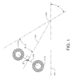
- Figure 1 illustrates a diagram of a first embodiment of the electrical connection system with the via holes fixed on an axis perpendicular to an axis that bisects the angle of misalignment of the connector boards.
- Misalignment angle A represents the angle of misalignment of top connector board 101 and bottom connector board 102.
- Bisecting axis 103 bisects angle A.
- Perpendicular axis 104 intersects bisecting axis 103 at intersection point P at an angle perpendicular to bisecting axis 103.
- Top surface via holes 111a and 112a are fixed along perpendicular axis 104 and are equidistant from intersection point P.
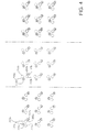
- the first column of Figure 2 illustrates a top view of the top surface of the PWB.
- Top surface mount pads 201a and 202a connect top daughter board connections 211a and 212a to via holes 111 and 112.
- the second column of Figure 2 illustrates a top view of the bottom surface of the PWB.
- Bottom surface mount pads 201b and 202b (shown by dashed lines) connect bottom daughter board connections 211b and 212b to via holes 111 and 112.
- the third column of Figure 2 illustrates a top view of the top surface and bottom surface of the PWB overlaid.
- Top first connection 211a is the outside connection on the top connector board
- bottom first connection 211b is the inside connection on the bottom connector board
- top second connection 212a is the inside connection on the top connector board
- bottom second connection 212b is the outside connection on the bottom connector board.
- the electrical path from the first top board connection 211a to the first bottom board connection 211b includes long top surface mount pad 201a and short bottom surface mount pad 201b.
- the electrical path from second top board connection 202a to second bottom board connection 202b includes short top surface mount pad 202a and long bottom surface mount pad 202b.
- both electrical paths consist of one long surface mount pad and one short surface mount pad. Both electrical paths are, therefore, of equal length. This ensures that the electrical signals transferred between electrical connections on each of the connector boards will not be out of phase.
- first top surface via hole 111a directly overlays first bottom surface via hole 111b and second top surface via hole 112a directly overlays second bottom surface via hole 112b.
- the electrical connection between via holes is straight through the mid-plane board at an angle perpendicular to faces of the mid-plane board. This allows for a straight through drilling procedure in construction of the mid-plane board.
- Figure 3 illustrates a diagram of a second embodiment of the electrical Connection system with the via holes fixed on an axis that bisects the angle of misalignment of the connector boards.
- Misalignment angle A represents the angle of misalignment of top connector board 101 and bottom connector board 102.
- Bisecting axis 103 bisects angle A.
- Top surface via holes 111a and 112a are fixed along bisecting axis 103.
- the first column of Figure 4 illustrates a top view of the top surface of the PWB.
- Top surface mount pads 201a and 202a connect top daughter board connections 211a and 212a to via holes 111 and 112.
- the second column of Figure 4 illustrates a top view of the bottom surface of the PWB.
- Bottom surface mount pads 201b and 202b (shown by dashed lines) connect bottom daughter board connections 211b and 212b to via holes 111 and 112.
- the third column of Figure 4 illustrates a top view of the top surface and bottom surface of the PWB overlaid.
- both first connections 211a,b are the outside connections
- both second connections 212a,b are the inside connections.
- this scheme is ideal for connecting boards oriented in directions such that the electrical signals travel from outside connections to outside connections and inside connections to inside connections.
- the electrical path from the first top board connection 211a to the first bottom board connection 211b includes top surface mount pad 201a and bottom surface mount pad 201b.
- the electrical path from second top board connection 212a to second bottom board connection 212b includes top surface mount pad 202a and bottom surface mount pad 202b.
- the length of all surface mount pads are equal because the distance from each via hole to each electrical connector is equal. All electrical paths are, therefore, of equal length.
- Figures 5-8 illustrate how the first routing scheme discussed generally in Figures 1 and 2 would be specifically implemented to the connection of two exemplary 5x8 headers on opposite sides of the mother board.
- Figure 5 illustrates a top view of the top surface of a mother board with two exemplary 5x8 headers on opposite sides of the mother board.
- Figure 6 illustrates a top view of the bottom surface of the mother board.
- Figure 7 illustrates a top view of the top surface and bottom surface of the mother board overlaid.
- the pattern in this case is a combination of two 4x4 patterns for a subtotal of 32 pairs.
- the 33 rd pair is the one of a kind pair in the top right corner of the diagrams.
- the 7 remaining pairs of the top most row and the right most column must be connected using the interlayer routing scheme shown in Figure 8.
Landscapes
- Engineering & Computer Science (AREA)
- Microelectronics & Electronic Packaging (AREA)
- Combinations Of Printed Boards (AREA)
- Coupling Device And Connection With Printed Circuit (AREA)
- Structure Of Printed Boards (AREA)
Abstract
Description
- The present invention relates to electrical connections of two printed circuit boards surface mounted on opposite sides of a mid-plane printed circuit board at angles to each other. Specifically, the invention is a routing scheme providing a direct electrical path between electrical connections.
- Modern electronic devices such as computers must be able to perform complex functions both quickly and effectively. Thus, it is essential that the internal hardware of these electrical devices is connected in an efficient manner. A common hardware assembly technique involves two printed circuit boards, commonly referred to as daughter boards, that are connected to opposite sides of a mid-plane printed circuit board, commonly referred to as a mother board. These daughter boards are often connected at angles to each other. For the electrical device to function as desired, the electrical components on one daughter board must be able to transmit and receive electrical signals to and from the electrical components on the other daughter board.
- There are several devices known in the prior art that provide such an electrical connection between two daughter boards. For example, Petit et al. describe in U.S. Patent No. 4,703,394 a system for interconnecting orthogonally disposed printed circuit boards. This system involves the use of four multiway connectors. Two of the connectors are mounted on respective facing edges of the connector boards, and two of the connectors are mounted on opposite sides of the mid-plane board. The connectors mounted on the connector boards plug into the connectors mounted on the mid-plane board.
- The interconnection system described in the Petit et al. requires the use of bulky connectors that makes its implementation undesirable in modern electrical devices which require a compact design.
- Sample et al. describe in U.S. Patent No. 5,887,158 a switching mid-plane and interconnecting system for interconnecting large numbers of signals. This system contains a mid-plane printed circuit board having a plurality of first connectors oriented in a first direction on one side of the mid-plane for making connections to the plurality of first printed-circuit boards. The mid-plane printed-circuit board also has a plurality of second connectors oriented in a second direction orthogonal to the plurality of first connectors on the other side of the mid-plane. The connectors are positioned such that connection pins on the plurality of first connectors and plurality of second connectors in regions of intersection are double-ended pins common to both. The remaining connection pins of the plurality of first connectors are single-ended connection pins which are connected to the single-ended connection pins of the plurality of second connectors via conductive traces on the mid-plane printed-circuit board.
- The interconnection system described in the Sample et al. is subject to two important drawbacks relating to the connection of the single ended connection pins. First, the electrical path connecting the single ended connection pins may vary in length. If the contacts are used for differential signals, this presents a problem because a longer electrical path may result in signals which are out of phase. Additionally, the electrical path connecting the single ended pins may run through the mother board diagonally rather than straight (at an angle perpendicular to the top and bottom side of the mother board). This diagonal electrical path presents a problem because it results in the entrance and exit of the electrical path into and out of the mother board to be misaligned, thereby creating the need for additional drilling in the mother board and further raising the complexity of the design.
- Thus, there is a need for a connection system that provides a routing scheme in which the electrical paths between connections in each pair of connections are of equal length. Furthermore, there is a need for a connection system that provides a routing scheme in which the electrical path runs straight through the mother board so that the entrance and exit of the electrical path into and out of the mother board directly overlay one another. Additionally, it is desired that this connection system is a compact system that does not require the use of bulky connector plug-ins. A connection system with these and other improve characteristics is desired.
- The present invention is an electrical connection system that includes two connector printed circuit boards surface mounted on opposite sides of a mid-plane printed circuit board at angles to each other. Each of the connector boards contains pairs of electrical connections. An electrical path connects each electrical connection on the first connector board to a corresponding electrical connection on the second connector board. This electrical path consists of three elements. The first element is preferably an electrically conductive surface mount pad connecting each electrical connection on the first connector board to a via hole on the first face of the mid-plane board. The second element is preferably a mid-plane electrical trace through two overlaying via holes on each face of the mid-plane board. This connection is straight through the mid-plane board at an angle perpendicular to each face of the board. The third element is preferably another electrically conductive surface mount pad connecting the via holes on the second face of the mid-plane board to the corresponding electrical connection on the second connector board.
- The length of the mid-plane electrical trace is preferably equal to the width of the mid-plane board. However, the length of the surface mount pads may vary provided that the total length of the electrical path connecting the first connections in each pair of electrical connections is equal to the total length of the electrical path connecting the second connections in the pair.
- In a preferred embodiment, each via hole in each pair is fixed on an axis perpendicular to an axis that bisects the angle of misalignment of the connector boards. Additionally, each via hole in each pair may be equidistant from a point on an axis that bisects the angle of misalignment of the connector boards. For the electrical paths connecting the first connections in each of the pairs of electrical connections, the first element will be a long surface mount pad and the third element will be a short surface mount pad. Conversely, for the electrical paths connecting the second connections in each of the pairs of electrical connections, the first element will be a short surface mount pad and the third element will be a long surface mount pad. Thus, the total length of the electrical path connecting the first connections in each pair of electrical connections is equal to the total length of the electrical path connecting the second connections in the pair.
- In a another preferred embodiment, each via hole in each pair is fixed directly on an axis that bisects the angle of misalignment of the connector boards. In this embodiment, all surface mount pads are equal in length. Thus, the total length of the electrical path connecting the first connections in each pair of electrical connections is equal to the total length of the electrical path connecting the second connections in the pair.
- The present invention will be better understood after reading the following detailed description of the presently preferred embodiments thereof with reference to the appended drawings, in which:
- Figure 1 illustrates a diagram of a first embodiment of the electrical connection system with the via holes fixed on an axis perpendicular to an axis that bisects the angle of misalignment of the connector boards.
- Figure 2 illustrates a diagram of the first embodiment adapted to a solder on surface mount connector where the front and backside daughter boards are orthogonal to each other.
- Figure 3 illustrates a diagram of the second embodiment of the electrical connection system with the via holes fixed on an axis that bisects the angle of misalignment of the connector boards.
- Figure 4 illustrates a diagram of the second embodiment adapted to a solder on surface mount connector where the front and backside daughter boards are orthogonal to each other.
- Figure 5 illustrates a top view of the top surface of a mother board with two exemplary 5x8 headers on opposite sides of the mother board.
- Figure 6 illustrates a top view of the bottom surface of a mother board with two exemplary 5x8 headers on opposite sides of the mother board.
- Figure 7 illustrates a top view of the top surface and bottom surface of a mother board overlaid with two exemplary 5x8 headers on opposite sides of the mother board.
- Figure 8 illustrates a view of the interlayer routing between unmatched pairs of connections of two exemplary 5x8 headers on opposite sides of the mother board.
-
- A system which meets the above-mentioned objects and provides other beneficial features in accordance with the presently preferred exemplary embodiment of the invention will be described below with reference to Figures 1-8. Those skilled in the art will readily appreciate that the description given herein with respect to those figures is for explanatory purposes only and is not intended in any way to limit the scope of the invention. Throughout the description, like reference numerals will refer to like elements in the respective figures.
- Figure 1 illustrates a diagram of a first embodiment of the electrical connection system with the via holes fixed on an axis perpendicular to an axis that bisects the angle of misalignment of the connector boards. Misalignment angle A represents the angle of misalignment of
top connector board 101 andbottom connector board 102.Bisecting axis 103 bisects angle A.Perpendicular axis 104 intersectsbisecting axis 103 at intersection point P at an angle perpendicular to bisectingaxis 103. Top surface viaholes perpendicular axis 104 and are equidistant from intersection point P. - Figure 2 illustrates a diagram of the first embodiment adapted to a solder on surface mount connector where the front and backside daughter boards are orthogonal (misalignment angle A = 90 degrees). The first column of Figure 2 illustrates a top view of the top surface of the PWB. Top
surface mount pads daughter board connections surface mount pads daughter board connections first connection 211a is the outside connection on the top connector board, and bottomfirst connection 211b is the inside connection on the bottom connector board. Conversely, topsecond connection 212a is the inside connection on the top connector board, and bottomsecond connection 212b is the outside connection on the bottom connector board. Thus, this scheme is ideal for connecting boards oriented in directions such that the electrical signals travel from outside connections to inside connections. - The electrical path from the first
top board connection 211a to the firstbottom board connection 211b includes long topsurface mount pad 201a and short bottomsurface mount pad 201b. The electrical path from secondtop board connection 202a to secondbottom board connection 202b includes short topsurface mount pad 202a and long bottomsurface mount pad 202b. As can be seen, both electrical paths consist of one long surface mount pad and one short surface mount pad. Both electrical paths are, therefore, of equal length. This ensures that the electrical signals transferred between electrical connections on each of the connector boards will not be out of phase. As may also be seen, first top surface viahole 111a directly overlays first bottom surface viahole 111b and second top surface viahole 112a directly overlays second bottom surface viahole 112b. Thus, the electrical connection between via holes is straight through the mid-plane board at an angle perpendicular to faces of the mid-plane board. This allows for a straight through drilling procedure in construction of the mid-plane board. - Figure 3 illustrates a diagram of a second embodiment of the electrical Connection system with the via holes fixed on an axis that bisects the angle of misalignment of the connector boards. Misalignment angle A represents the angle of misalignment of
top connector board 101 andbottom connector board 102.Bisecting axis 103 bisects angle A. Top surface viaholes axis 103. - Figure 4 illustrates a diagram of a second embodiemnt adapted to a solder on surface mount connector where the front and backside daughter boards are orthogonal (misalignment angle A = 90 degrees). The first column of Figure 4 illustrates a top view of the top surface of the PWB. Top
surface mount pads daughter board connections surface mount pads daughter board connections first connections 211a,b are the outside connections, and bothsecond connections 212a,b are the inside connections. Thus, this scheme is ideal for connecting boards oriented in directions such that the electrical signals travel from outside connections to outside connections and inside connections to inside connections. - The electrical path from the first
top board connection 211a to the firstbottom board connection 211b includes topsurface mount pad 201a and bottomsurface mount pad 201b. The electrical path from secondtop board connection 212a to secondbottom board connection 212b includes topsurface mount pad 202a and bottomsurface mount pad 202b. In this scheme, the length of all surface mount pads are equal because the distance from each via hole to each electrical connector is equal. All electrical paths are, therefore, of equal length. - Figures 5-8 illustrate how the first routing scheme discussed generally in Figures 1 and 2 would be specifically implemented to the connection of two exemplary 5x8 headers on opposite sides of the mother board. This illustration is for exemplary purposes only and is no way intended to limit the scope of this invention. Figure 5 illustrates a top view of the top surface of a mother board with two exemplary 5x8 headers on opposite sides of the mother board. Figure 6 illustrates a top view of the bottom surface of the mother board. Figure 7 illustrates a top view of the top surface and bottom surface of the mother board overlaid. There is a total of 40 pairs of connections. However, as is apparent from an examination of Figures 5-7, the routing scheme of this invention can only be applied to 33 of the 40 total pairs. The pattern in this case is a combination of two 4x4 patterns for a subtotal of 32 pairs. The 33rd pair is the one of a kind pair in the top right corner of the diagrams. The 7 remaining pairs of the top most row and the right most column must be connected using the interlayer routing scheme shown in Figure 8. While the invention has been described and illustrated with reference to specific embodiments, those skilled in the art will recognize that modification and variations may be made without departing from the principles of the invention as described above and set forth in the following claims. For example, while the invention has been described as being used to connect orthogonal first and second printed circuit boards, the invention may be used to connect printed circuit boards at any angle of misalignment. Furthermore, first and second printed circuit boards may contain any size pattern of connections and is not intended to be limited to a five by eight pattern of connections. Accordingly, reference should be made to the appended claims as indicating the scope of the invention.
Claims (20)
- A routing system for interconnecting two surface mounted printed circuit boards comprising:a mid-plane printed circuit board including a first face and a second face, said second face parallel to said first face;a first printed circuit board surface (101) mounted on said first face of said mid-plane printed circuit board, said first printed circuit board containing pairs of electrical connections (211a, 212a);a second printed circuit board surface (102) mounted on said second face of said mid-plane printed circuit board, said second printed circuit board containing pairs of electrical connections (211b, 212b), said second printed circuit boards mounted at an angle to said first printed circuit boards;a plurality of pairs of via holes (111a, 112a; 111b, 112b) on said first and second faces of said mid-plane printed circuit board positioned with respect to the angle of misalignment (A) of said first and second printed circuit boards, said pairs of via holes (111a, 112a) on said first face of said mid-plane printed circuit board directly overlaying said pairs of via holes (111b, 112b) on said second face of said mid-plane printed circuit board; anda plurality of electrical paths (201a, 202a; 201b, 202b) through said overlaying pairs of via holes connecting said pairs of electrical connections on said first printed circuit board to said electrical connections on said second printed circuit board.
- A system according to claim 1, wherein said pairs of via holes are positioned such that:A. each via hole in each of said pairs of via holes is fixed on an axis perpendicular to an axis (103) that bisects the angle of misalignment (A) of said first and second printed circuit boards; andB. both via holes in each of said pairs of via holes are equidistant from a point (P) on an axis that bisects the angle of misalignment of said first and second printed circuit boards.
- A system according to claim 1, wherein said pairs of via holes are positioned such that:A. each via hole in each of said pairs of via holes is fixed on an axis (103) that bisects the angle of misalignment (A) of said first and second printed circuit boards; andB. The distance between the first via hole (111a) in each of said pairs of via holes and the first electrical connection (211a) in one of said pairs of electrical connections is equal to the distance between the second via hole (111b) in each of said pairs of via holes and the second electrical connection (211b) in one of said pairs of electrical connections.
- A system according to claim 3, wherein said electrical paths (201a, 202a; 201b, 202b) are substantially equal in length.
- A system according to claim 3. wherein said electrical paths (201a, 202a; 201b, 202b) consist of:a first face electrically conductive surface mount pad mounted on said first face of said mid-plane printed circuit board connecting one of said electrical connections on said first printed circuit board to one of said via holes on said first face of said mid-plane printed circuit board;an electrically conductive trace connecting each of said via holes on said second face of said mid-plane printed circuit board with the directly overlaying via hole on said first face of said mid-plane printed circuit board; anda second face electrically conductive surface mount pads mounted on said second face of said mid-plane printed circuit board connecting one of said electrical connections on said second printed circuit board to one of said via holes on said second face of said mid-plane printed circuit board.
- A system according to claim 5, wherein said electrically conductive traces pass straight through said mid-plane printed circuit board at an angle perpendicular to said mid-plane printed circuit board.
- A system according to claim 5, wherein said electrically conductive traces are substantially equal in length.
- A system according to claim 5, wherein said first face electrically conductive surface mount pads are substantially equal in length.
- A system according to claim 5, wherein said second face electrically conductive surface mount pads are substantially equal in length.
- A system according to claim 5, wherein said first face electrically conductive surface mount pads are substantially equal in length to said second face electrically conductive surface mount pads.
- A system according to claim 5, wherein each of said first face surface mount pads (201a) connecting the first electrical connection (211a) in each of said pairs of electrical connections is a long surface mount pad and each of said first face surface mount pads connecting the second electrical connection in each of said pairs of electrical connections is a short surface mount pad.
- A system according to claim 11, wherein each of said long surface mount pads is substantially equal in length.
- A system according to claim 11, wherein each of said short surface mount pads is substantially equal in length.
- A system according to claim 5, wherein each of said second face surface mount pads (202a) connecting the first electrical connection (212a) in each of said pairs of electrical connections is a short surface mount pad and each of said second face surface mount pads connecting the second electrical connection in each of said pairs of electrical connections is a long surface mount pad.
- A system according to claim 14, wherein each of said long surface mount pads is substantially equal in length.
- A system according to claim 14, wherein each of said short surface mount pads is substantially equal in length.
- A system according to claim 1, wherein said first and second printed circuit boards are orthogonal.
- A system according to claim 1, wherein said first and second printed circuit boards are five by eight headers.
- A system according to claim 1 for interconnecting two surface mounted printed circuit boards comprising:a mid-plane printed circuit board including a first face and a second face, said second face parallel to said first face;a first printed circuit board surface (101) mounted on said first face of said mid-plane printed circuit board, said first printed circuit board containing pairs of electrical connections;a second printed circuit board surface (102) mounted on said second face of said mid-plane printed circuit board, said second printed circuit board containing pairs of electrical connections, said second printed circuit boards mounted at an angle to said first printed circuit boards;a plurality of pairs of via holes (111a, 112a; 111b, 112b) on said first and second faces of said mid-plane printed circuit board positioned such that:A. Each via hole in each of said pairs of via holes is fixed on an axis perpendicular to an axis (103) that bisects the angle of misalignment (A) of said first and second printed circuit boards;B. Both via holes in each of said pairs of via holes is equidistant from a point (P) on an axis that bisects the angle of misalignment of said first and second printed circuit boards; andC. Each of said pairs of via holes on said first face of said mid-plane printed circuit board is directly overlaying one of said pairs of via holes on said second face of said mid-plane printed circuit board;a plurality of electrically conductive traces (201a, 202a; 201b, 202b) connecting each of said via holes in said pairs of via hole on said second face of said mid-plane printed circuit board one of said directly overlaying via holes in said pairs of via holes on said first face of said mid-plane printed circuit board, said electrically conductive traces being substantially equal in length;a plurality of long first face electrically conductive surface mount pads (201a) mounted on said first face of said mid-plane printed circuit board, said long first face electrically conductive surface mount pads connecting the first connection in each of said pairs of electrical connections on said first printed circuit board to the first via hole (111a) in each of said pairs of via holes on said first face of said mid-plane printed circuit board, said long first face electrically conductive surface mount pads being substantially equal in length;a plurality of short first face electrically conductive surface mount pads (202a) mounted on said first face of said mid-plane printed circuit board, said short first face electrically conductive surface mount pads connecting the second connection in each of said pairs of electrical connections on said first printed circuit board to the second via hole (112a) in each of said pairs of via holes on said first face of said mid-plane printed circuit board, said short first face electrically conductive surface mount pads being substantially equal in length;a plurality of short second face electrically conductive surface mount pads (201b) mounted on said second face of said mid-plane printed circuit board, said short second face electrically conductive surface mount pads connecting the first connection in each of said pairs of electrical connections on said second printed circuit board to the first via hole (111b) in each of said pairs of via holes on said second face of said mid-plane printed circuit board, said short second face electrically conductive surface mount pads being substantially equal in length; anda plurality of long second face electrically conductive surface mount pads (202b) mounted on said second face of said mid-plane printed circuit board, each of said long second face electrically conductive surface mount pads connecting the second connection in each of said pairs of electrical connections on said second printed circuit board to the second via hole (112b) in each of said pairs via holes on said second face of said mid-plane printed circuit board, said long second face electrically conductive surface mount pads being substantially equal in length.
- A system according to claim 1 for interconnecting two surface mounted printed circuit boards comprising:a mid-plane printed circuit board including a first face and a second face, said second face parallel to said first face;a first printed circuit board surface (101) mounted on said first face of said mid-plane printed circuit board, said first printed circuit board containing pairs of electrical connections;a second printed circuit board surface (102) mounted on said second face of said mid-plane printed circuit board, said second printed circuit board containing pairs of electrical connections, said second printed circuit boards mounted at an angle to said first printed circuit boards;a plurality of pairs of via holes (111a, 112a; 111b, 112b) on said first and second faces of said mid-plane printed circuit board positioned such that:A. each via hole in each of said second face pairs of via holes is fixed on an axis (103) that bisects the angle of misalignment (A) of said first and second printed circuit boards:B. The distance between the first via hole (111a) in each of said second face pairs of via holes and the first electrical connection (211a) in one of said pairs of electrical connections on said second printed circuit board is equal to the distance between the second via hole (111b) in each of said second face pairs of via holes and the second electrical connection (211b) in one of said pairs of electrical connections on said second printed circuit board; andC. each of said pairs of via holes on said first face of said mid-plane printed circuit board is directly overlaying one of said pairs of via holes on said second face of said mid-plane printed circuit board;a plurality of electrically conductive traces (201a, 202a; 201b, 202b) connecting each of said via holes in said pairs of via hole on said second face of said mid-plane printed circuit board one of said directly overlaying via holes in said pairs of via holes on said first face of said mid-plane printed circuit board, said electrically conductive traces being substantially equal in length;a plurality of first face electrically conductive surface mount pads (201a, 202a) mounted on said first face of said mid-plane printed circuit board, each of said first face electrically conductive surface mount pads connecting one of said electrical connections on said first printed circuit board to one of said via holes (111a, 112a) on said first face of said mid-plane printed circuit board, said first face electrically conductive traces being substantially equal in length; anda plurality of second face electrically conductive surface mount pads (201b, 202b) mounted on said second face of said mid-plane printed circuit board, each of said second face electrically conductive surface mount pads connecting one of said electrical connections on said second printed circuit board to one of said via holes (111b, 112b) on said second face of said mid-plane printed circuit board, said second face electrically conductive traces being substantially equal in length to said first face electrically conductive traces.
Applications Claiming Priority (2)
| Application Number | Priority Date | Filing Date | Title |
|---|---|---|---|
| US51703 | 2002-01-18 | ||
| US10/051,703 US6717825B2 (en) | 2002-01-18 | 2002-01-18 | Electrical connection system for two printed circuit boards mounted on opposite sides of a mid-plane printed circuit board at angles to each other |
Publications (2)
| Publication Number | Publication Date |
|---|---|
| EP1330145A2 true EP1330145A2 (en) | 2003-07-23 |
| EP1330145A3 EP1330145A3 (en) | 2005-08-10 |
Family
ID=21972851
Family Applications (1)
| Application Number | Title | Priority Date | Filing Date |
|---|---|---|---|
| EP03000693A Withdrawn EP1330145A3 (en) | 2002-01-18 | 2003-01-17 | Electrical connection system for two printed circuit boards mounted on opposite sides of a mid-plane printed circuit board at angles to each other |
Country Status (6)
| Country | Link |
|---|---|
| US (1) | US6717825B2 (en) |
| EP (1) | EP1330145A3 (en) |
| JP (1) | JP2003243793A (en) |
| KR (1) | KR20030063170A (en) |
| CN (1) | CN1284427C (en) |
| CA (1) | CA2415934A1 (en) |
Cited By (3)
| Publication number | Priority date | Publication date | Assignee | Title |
|---|---|---|---|---|
| WO2005074336A3 (en) * | 2004-01-26 | 2005-10-06 | Litton Systems Inc | Multilayered circuit board for high-speed, differential signals |
| EP1831970A4 (en) * | 2004-12-24 | 2013-04-24 | Amphenol Corp | Midplane epecially applicable to an ortogonal architecture electronic system |
| US8444436B1 (en) | 2004-07-01 | 2013-05-21 | Amphenol Corporation | Midplane especially applicable to an orthogonal architecture electronic system |
Families Citing this family (62)
| Publication number | Priority date | Publication date | Assignee | Title |
|---|---|---|---|---|
| US7524209B2 (en) | 2003-09-26 | 2009-04-28 | Fci Americas Technology, Inc. | Impedance mating interface for electrical connectors |
| US7094102B2 (en) | 2004-07-01 | 2006-08-22 | Amphenol Corporation | Differential electrical connector assembly |
| US7281950B2 (en) * | 2004-09-29 | 2007-10-16 | Fci Americas Technology, Inc. | High speed connectors that minimize signal skew and crosstalk |
| US20060073709A1 (en) * | 2004-10-06 | 2006-04-06 | Teradyne, Inc. | High density midplane |
| US7284221B2 (en) * | 2004-11-29 | 2007-10-16 | Fci Americas Technology, Inc. | High-frequency, high-signal-density, surface-mount technology footprint definitions |
| CN101673885B (en) * | 2004-11-29 | 2012-07-18 | Fci公司 | Improved Matched Impedance Surface Mount Technology Footprint |
| US7709747B2 (en) * | 2004-11-29 | 2010-05-04 | Fci | Matched-impedance surface-mount technology footprints |
| JP4498181B2 (en) * | 2005-03-22 | 2010-07-07 | 東京エレクトロン株式会社 | Switch array |
| US20060228912A1 (en) * | 2005-04-07 | 2006-10-12 | Fci Americas Technology, Inc. | Orthogonal backplane connector |
| US7914304B2 (en) * | 2005-06-30 | 2011-03-29 | Amphenol Corporation | Electrical connector with conductors having diverging portions |
| US20090291593A1 (en) | 2005-06-30 | 2009-11-26 | Prescott Atkinson | High frequency broadside-coupled electrical connector |
| US7331802B2 (en) | 2005-11-02 | 2008-02-19 | Tyco Electronics Corporation | Orthogonal connector |
| CN100518442C (en) * | 2006-07-17 | 2009-07-22 | 英业达股份有限公司 | Wiring method and system |
| US7500871B2 (en) * | 2006-08-21 | 2009-03-10 | Fci Americas Technology, Inc. | Electrical connector system with jogged contact tails |
| US7713088B2 (en) | 2006-10-05 | 2010-05-11 | Fci | Broadside-coupled signal pair configurations for electrical connectors |
| US7708569B2 (en) | 2006-10-30 | 2010-05-04 | Fci Americas Technology, Inc. | Broadside-coupled signal pair configurations for electrical connectors |
| US7497736B2 (en) | 2006-12-19 | 2009-03-03 | Fci Americas Technology, Inc. | Shieldless, high-speed, low-cross-talk electrical connector |
| US7811100B2 (en) | 2007-07-13 | 2010-10-12 | Fci Americas Technology, Inc. | Electrical connector system having a continuous ground at the mating interface thereof |
| US8251745B2 (en) * | 2007-11-07 | 2012-08-28 | Fci Americas Technology Llc | Electrical connector system with orthogonal contact tails |
| US7654870B2 (en) * | 2008-02-11 | 2010-02-02 | Z-Plane, Inc. | Interconnection assembly for printed circuit boards |
| US8764464B2 (en) | 2008-02-29 | 2014-07-01 | Fci Americas Technology Llc | Cross talk reduction for high speed electrical connectors |
| US7758385B2 (en) * | 2008-03-07 | 2010-07-20 | Tyco Electronics Corporation | Orthogonal electrical connector and assembly |
| US8545240B2 (en) | 2008-11-14 | 2013-10-01 | Molex Incorporated | Connector with terminals forming differential pairs |
| MY155071A (en) | 2008-12-12 | 2015-08-28 | Molex Inc | Resonance modifying connector |
| US7988456B2 (en) * | 2009-01-14 | 2011-08-02 | Tyco Electronics Corporation | Orthogonal connector system |
| US7883366B2 (en) * | 2009-02-02 | 2011-02-08 | Tyco Electronics Corporation | High density connector assembly |
| US9277649B2 (en) | 2009-02-26 | 2016-03-01 | Fci Americas Technology Llc | Cross talk reduction for high-speed electrical connectors |
| US8366485B2 (en) | 2009-03-19 | 2013-02-05 | Fci Americas Technology Llc | Electrical connector having ribbed ground plate |
| US8079847B2 (en) * | 2009-06-01 | 2011-12-20 | Tyco Electronics Corporation | Orthogonal connector system with power connection |
| US8267721B2 (en) | 2009-10-28 | 2012-09-18 | Fci Americas Technology Llc | Electrical connector having ground plates and ground coupling bar |
| US8616919B2 (en) | 2009-11-13 | 2013-12-31 | Fci Americas Technology Llc | Attachment system for electrical connector |
| SG181953A1 (en) * | 2009-12-30 | 2012-07-30 | Framatome Connectors Int | Electrical connector having impedence tuning ribs |
| WO2011140438A2 (en) | 2010-05-07 | 2011-11-10 | Amphenol Corporation | High performance cable connector |
| US9136634B2 (en) | 2010-09-03 | 2015-09-15 | Fci Americas Technology Llc | Low-cross-talk electrical connector |
| US8657627B2 (en) | 2011-02-02 | 2014-02-25 | Amphenol Corporation | Mezzanine connector |
| US8827746B2 (en) * | 2011-08-01 | 2014-09-09 | Z-Plane, Inc. | Crosstalk reduction |
| US9137887B2 (en) * | 2011-09-07 | 2015-09-15 | Samtec, Inc. | Via structure for transmitting differential signals |
| EP2761981B1 (en) * | 2011-09-30 | 2017-12-13 | Airbus Operations S.A.S. | Electrical cabinet for an aircraft, including an improved electrical connection system |
| EP2624034A1 (en) | 2012-01-31 | 2013-08-07 | Fci | Dismountable optical coupling device |
| USD727852S1 (en) | 2012-04-13 | 2015-04-28 | Fci Americas Technology Llc | Ground shield for a right angle electrical connector |
| USD718253S1 (en) | 2012-04-13 | 2014-11-25 | Fci Americas Technology Llc | Electrical cable connector |
| USD727268S1 (en) | 2012-04-13 | 2015-04-21 | Fci Americas Technology Llc | Vertical electrical connector |
| US9257778B2 (en) | 2012-04-13 | 2016-02-09 | Fci Americas Technology | High speed electrical connector |
| US8944831B2 (en) | 2012-04-13 | 2015-02-03 | Fci Americas Technology Llc | Electrical connector having ribbed ground plate with engagement members |
| US9543703B2 (en) | 2012-07-11 | 2017-01-10 | Fci Americas Technology Llc | Electrical connector with reduced stack height |
| USD751507S1 (en) | 2012-07-11 | 2016-03-15 | Fci Americas Technology Llc | Electrical connector |
| CN104704682B (en) | 2012-08-22 | 2017-03-22 | 安费诺有限公司 | High-frequency electrical connector |
| USD745852S1 (en) | 2013-01-25 | 2015-12-22 | Fci Americas Technology Llc | Electrical connector |
| DE102013203661A1 (en) | 2013-03-04 | 2014-09-04 | Robert Bosch Gmbh | Method for operating an electrified motor vehicle and means for implementing it |
| USD720698S1 (en) | 2013-03-15 | 2015-01-06 | Fci Americas Technology Llc | Electrical cable connector |
| WO2015112717A1 (en) | 2014-01-22 | 2015-07-30 | Amphenol Corporation | High speed, high density electrical connector with shielded signal paths |
| US10541482B2 (en) | 2015-07-07 | 2020-01-21 | Amphenol Fci Asia Pte. Ltd. | Electrical connector with cavity between terminals |
| TWI790798B (en) | 2016-08-23 | 2023-01-21 | 美商安芬諾股份有限公司 | Connector configurable for high performance |
| CN110740569A (en) * | 2018-07-19 | 2020-01-31 | 鸿富锦精密工业(武汉)有限公司 | A printed circuit board |
| CN208862209U (en) | 2018-09-26 | 2019-05-14 | 安费诺东亚电子科技(深圳)有限公司 | A kind of connector and its pcb board of application |
| CN112930628B (en) | 2018-10-25 | 2024-02-20 | 申泰公司 | Hybrid electrical connectors for high frequency signals |
| TW202439723A (en) | 2019-02-19 | 2024-10-01 | 美商安芬諾股份有限公司 | Electrical connector and method for manufacturing electrical connector |
| TW202534957A (en) | 2020-01-27 | 2025-09-01 | 美商Fci美國有限責任公司 | High speed, high density direct mate orthogonal connector |
| TW202607982A (en) | 2020-01-27 | 2026-02-16 | 美商Fci美國有限責任公司 | Electrical connector |
| CN215816516U (en) | 2020-09-22 | 2022-02-11 | 安费诺商用电子产品(成都)有限公司 | Electrical connector |
| CN213636403U (en) | 2020-09-25 | 2021-07-06 | 安费诺商用电子产品(成都)有限公司 | Electrical connector |
| CN215266741U (en) | 2021-08-13 | 2021-12-21 | 安费诺商用电子产品(成都)有限公司 | High-performance card connector meeting high-bandwidth transmission |
Family Cites Families (17)
| Publication number | Priority date | Publication date | Assignee | Title |
|---|---|---|---|---|
| US3552123A (en) * | 1969-06-26 | 1971-01-05 | United Aircraft Corp | Sequential fuel control |
| US3680037A (en) * | 1970-11-05 | 1972-07-25 | Tech Wire Prod Inc | Electrical interconnector |
| US4472765A (en) * | 1982-09-13 | 1984-09-18 | Hughes Electronic Devices Corporation | Circuit structure |
| US5019945A (en) * | 1983-05-31 | 1991-05-28 | Trw Inc. | Backplane interconnection system |
| US4575780A (en) | 1984-04-03 | 1986-03-11 | Northern Telecom Limited | Backpanel assemblies |
| FR2589286B1 (en) | 1985-10-25 | 1988-05-13 | Cit Alcatel | ORTHOGONAL PRINTED CIRCUIT BOARD INTERCONNECTION ASSEMBLY AND SWITCHING NETWORKS USING THE SAME |
| US4838798A (en) | 1988-06-15 | 1989-06-13 | Amp Incorporated | High density board to board interconnection system |
| US4907977A (en) | 1988-10-14 | 1990-03-13 | Ncr Corporation | Computer backpanel inversion coupler |
| SE466282B (en) | 1989-10-02 | 1992-01-20 | Ericsson Telefon Ab L M | FUNCTIONAL UNIT FOR ELECTRONIC EQUIPMENT |
| US5335146A (en) | 1992-01-29 | 1994-08-02 | International Business Machines Corporation | High density packaging for device requiring large numbers of unique signals utilizing orthogonal plugging and zero insertion force connetors |
| US5352123A (en) | 1992-06-08 | 1994-10-04 | Quickturn Systems, Incorporated | Switching midplane and interconnection system for interconnecting large numbers of signals |
| CA2124773C (en) | 1994-05-31 | 1998-11-03 | Raymond Bruce Wallace | Backplane and shelf |
| US5926378A (en) | 1995-09-29 | 1999-07-20 | International Business Machines Corporation | Low profile riser card assembly using paired back-to-back peripheral card connectors mounted on universal footprints supporting different bus form factors |
| US5815374A (en) * | 1996-09-30 | 1998-09-29 | International Business Machines Corporation | Method and apparatus for redirecting certain input/output connections of integrated circuit chip configurations |
| US6163462A (en) * | 1997-12-08 | 2000-12-19 | Analog Devices, Inc. | Stress relief substrate for solder ball grid array mounted circuits and method of packaging |
| US6528737B1 (en) * | 2000-08-16 | 2003-03-04 | Nortel Networks Limited | Midplane configuration featuring surface contact connectors |
| US6538899B1 (en) * | 2001-01-02 | 2003-03-25 | Juniper Networks, Inc. | Traceless midplane |
-
2002
- 2002-01-18 US US10/051,703 patent/US6717825B2/en not_active Expired - Lifetime
-
2003
- 2003-01-08 CA CA002415934A patent/CA2415934A1/en not_active Abandoned
- 2003-01-17 EP EP03000693A patent/EP1330145A3/en not_active Withdrawn
- 2003-01-17 KR KR10-2003-0003172A patent/KR20030063170A/en not_active Ceased
- 2003-01-17 JP JP2003009541A patent/JP2003243793A/en not_active Withdrawn
- 2003-01-17 CN CNB03101710XA patent/CN1284427C/en not_active Expired - Fee Related
Non-Patent Citations (1)
| Title |
|---|
| None |
Cited By (5)
| Publication number | Priority date | Publication date | Assignee | Title |
|---|---|---|---|---|
| WO2005074336A3 (en) * | 2004-01-26 | 2005-10-06 | Litton Systems Inc | Multilayered circuit board for high-speed, differential signals |
| US7057115B2 (en) | 2004-01-26 | 2006-06-06 | Litton Systems, Inc. | Multilayered circuit board for high-speed, differential signals |
| US8444436B1 (en) | 2004-07-01 | 2013-05-21 | Amphenol Corporation | Midplane especially applicable to an orthogonal architecture electronic system |
| US9106020B2 (en) | 2004-07-01 | 2015-08-11 | Amphenol Corporation | Midplane especially applicable to an orthogonal architecture electronic system |
| EP1831970A4 (en) * | 2004-12-24 | 2013-04-24 | Amphenol Corp | Midplane epecially applicable to an ortogonal architecture electronic system |
Also Published As
| Publication number | Publication date |
|---|---|
| KR20030063170A (en) | 2003-07-28 |
| CN1433254A (en) | 2003-07-30 |
| EP1330145A3 (en) | 2005-08-10 |
| CN1284427C (en) | 2006-11-08 |
| CA2415934A1 (en) | 2003-07-18 |
| JP2003243793A (en) | 2003-08-29 |
| US20030137817A1 (en) | 2003-07-24 |
| US6717825B2 (en) | 2004-04-06 |
Similar Documents
| Publication | Publication Date | Title |
|---|---|---|
| US6717825B2 (en) | Electrical connection system for two printed circuit boards mounted on opposite sides of a mid-plane printed circuit board at angles to each other | |
| US12218462B2 (en) | High-frequency electrical connector | |
| US6287132B1 (en) | Connector with staggered contact design | |
| CN101120491B (en) | Midplane particularly suited for orthogonal architecture electronic systems | |
| US6824391B2 (en) | Electrical connector having customizable circuit board wafers | |
| US6336827B1 (en) | Balanced-transmission cable-and-connector unit | |
| US6641411B1 (en) | Low cost high speed connector | |
| CN1182630C (en) | Electrical connector including a housing supporting parallel circuit boards | |
| US6633490B2 (en) | Electronic board assembly including two elementary boards each carrying connectors on an edge thereof | |
| CN101120490B (en) | Differential electrical connector assembly | |
| US4618196A (en) | Gender reversal connector | |
| CN108140968B (en) | Connector system with adapter | |
| US6416333B1 (en) | Extension boards and method of extending boards | |
| US20020060906A1 (en) | Interconnecting method of wiring in printed circuit boards and printed circuit board unit | |
| US4859190A (en) | Dual connector printed circuit board assembly and method | |
| US6818838B1 (en) | PCB component placement and trace routing therebetween | |
| US20250386426A1 (en) | Electronic circuit board | |
| KR100505641B1 (en) | Memory module and memory system having the same | |
| US6118669A (en) | Routing topology for identical connector point layouts on primary and secondary sides of a substrate | |
| JP2000012130A (en) | Connector structure | |
| JP2002124742A (en) | Printed wiring boards, connecting parts, and electronic devices | |
| JPH01313866A (en) | Three-dimensionally mounted male connector | |
| JPH08316595A (en) | Flexible circuit board | |
| US20070207632A1 (en) | Midplane with offset connectors | |
| JPS62265797A (en) | Backboard structure |
Legal Events
| Date | Code | Title | Description |
|---|---|---|---|
| PUAI | Public reference made under article 153(3) epc to a published international application that has entered the european phase |
Free format text: ORIGINAL CODE: 0009012 |
|
| AK | Designated contracting states |
Designated state(s): AT BE BG CH CY CZ DE DK EE ES FI FR GB GR HU IE IT LI LU MC NL PT SE SI SK TR |
|
| AX | Request for extension of the european patent |
Extension state: AL LT LV MK RO |
|
| PUAL | Search report despatched |
Free format text: ORIGINAL CODE: 0009013 |
|
| AK | Designated contracting states |
Kind code of ref document: A3 Designated state(s): AT BE BG CH CY CZ DE DK EE ES FI FR GB GR HU IE IT LI LU MC NL PT SE SI SK TR |
|
| AX | Request for extension of the european patent |
Extension state: AL LT LV MK RO |
|
| 17P | Request for examination filed |
Effective date: 20051107 |
|
| AKX | Designation fees paid |
Designated state(s): AT BE BG CH CY CZ DE DK EE ES FI FR GB GR HU IE IT LI LU MC NL PT SE SI SK TR |
|
| 17Q | First examination report despatched |
Effective date: 20081216 |
|
| RAP1 | Party data changed (applicant data changed or rights of an application transferred) |
Owner name: FCI |
|
| APBK | Appeal reference recorded |
Free format text: ORIGINAL CODE: EPIDOSNREFNE |
|
| APBN | Date of receipt of notice of appeal recorded |
Free format text: ORIGINAL CODE: EPIDOSNNOA2E |
|
| APBR | Date of receipt of statement of grounds of appeal recorded |
Free format text: ORIGINAL CODE: EPIDOSNNOA3E |
|
| APAF | Appeal reference modified |
Free format text: ORIGINAL CODE: EPIDOSCREFNE |
|
| APBT | Appeal procedure closed |
Free format text: ORIGINAL CODE: EPIDOSNNOA9E |
|
| STAA | Information on the status of an ep patent application or granted ep patent |
Free format text: STATUS: THE APPLICATION IS DEEMED TO BE WITHDRAWN |
|
| 18D | Application deemed to be withdrawn |
Effective date: 20140415 |