EP1329939A1 - Photomultiplier - Google Patents
Photomultiplier Download PDFInfo
- Publication number
- EP1329939A1 EP1329939A1 EP01951938A EP01951938A EP1329939A1 EP 1329939 A1 EP1329939 A1 EP 1329939A1 EP 01951938 A EP01951938 A EP 01951938A EP 01951938 A EP01951938 A EP 01951938A EP 1329939 A1 EP1329939 A1 EP 1329939A1
- Authority
- EP
- European Patent Office
- Prior art keywords
- dynodes
- support portions
- dynode
- secondary electron
- electron emitting
- Prior art date
- Legal status (The legal status is an assumption and is not a legal conclusion. Google has not performed a legal analysis and makes no representation as to the accuracy of the status listed.)
- Granted
Links
Images


Classifications
-
- H—ELECTRICITY
- H01—ELECTRIC ELEMENTS
- H01J—ELECTRIC DISCHARGE TUBES OR DISCHARGE LAMPS
- H01J43/00—Secondary-emission tubes; Electron-multiplier tubes
- H01J43/04—Electron multipliers
- H01J43/06—Electrode arrangements
- H01J43/18—Electrode arrangements using essentially more than one dynode
- H01J43/20—Dynodes consisting of sheet material, e.g. plane, bent
Definitions
- the present invention relates to a photomultiplier tube, and particularly to a photomultiplier tube with excellent vibration resistance.
- a photomultiplier tube disclosed in Japanese unexamined patent application publication No. HEI-9-180670 is provided with two support portions protruding one from each end of the second and third dynodes. More specifically, these dynodes are configured from a concave plate part, forming the secondary electron emitting surface, and two upper and lower support plate parts extending from the top and bottom ends of the concave plate part toward the back side thereof. Support portions are formed on both ends of each of the top and bottom support plate parts. Holes are formed in each of two ceramic base plates for engaging the support portions on the two dynodes. Each support portion is supported by inserting the support portions into the corresponding holes and sandwiching each dynode between the two ceramic base plates.
- two support portions are formed on both ends of each dynode, extending along the same plane.
- a single slit corresponding to the two support portions on each dynode is formed in the two base plates.
- the two support portions are fixed in the base plates by inserting the support portions into the corresponding single slit and bending over the ends of the support portions.
- the photomultiplier tube includes a tube-shaped vacuum vessel extending along the tube axis; a photocathode positioned on one end of the tube-shaped vacuum vessel in relation to the tube axis for converting incident light to electrons; a pair of electrically insulating base plates; dynodes of a plurality of stages interposed between the pair of base plates and having secondary electron emitting surfaces formed on their inner walls for multiplying electrons sequentially; and an anode for receiving the electrons multiplied by the plurality of stages of dynodes.
- At least one dynode from among the dynodes of the plurality of stages is formed of planar first support portions extending outward from both ends of the secondary electron emitting surface on the base plate side; planar second support portions also extending outward from both ends of the secondary electron emitting surface on the base plate side and forming a prescribed angle with the first support portions; first through-holes formed in the pair of base plates for inserting the first support portions; and second through-holes formed in the pair of base plates for inserting the second support portions.
- the first and second support portions are formed at a prescribed angle in relation to each other. Therefore, rattling of the dynode in the direction of rotation about one support portion is restricted by the other support portion. Even when rattling is generated due to clearance, play, or the like provided for inserting the dynode into the through-holes of the base plate, the directivity and play of the rattling in one support portion is restricted by the other support portion, thereby enabling the dynodes to be reliably and fixedly supported.
- the second support portions are formed shorter than the thickness of the base plates. Hence, the second support portions do not protrude from the outer surfaces of the base plates.
- the second support portions do not protrude from the base plates when the dynodes are supported therein. Only the first support portions protrude from the base plates. Accordingly, power can be supplied to the dynodes via the first support portions protruding from the outside of the base plates, without wiring or the like interfering with each other. By eliminating the crowding of support portions, the problem of voltage proof destruction caused by support portions of different dynodes being placed close to one another does not occur.
- side surface portions disposed perpendicular to the secondary electron emitting surface are formed on both ends of the secondary electron emitting surface near the base plate in at least one dynode.
- the first support portions are formed on top of the side surface portions.
- the side surface portions are provided on both ends of the secondary electron emitting surface in the lengthwise direction, thereby preventing electrons from colliding directly with the base plate and charging up the same.
- the electron trajectories converge on the inner surface due to the potential on both side surface portions.
- the first support portions are provided on both side surface portions, and the second support portions form a prescribed angle with the first support portions, rattling relative to the first and second support portions is restrained by the side surface portions, thereby more effectively preventing rattling.
- lugs can be formed in an approximate central position on the first or second support portions in the thickness dimension thereof.
- the resulting ear parts can be pressed into the corresponding through-holes to fix the dynodes to the base plates satisfactorily.
- the photomultiplier tube of the present invention it is possible to provide a shielding plate between the dynode of the first stage and the dynodes of the (n-3) th through n th stages.
- This construction can prevent light and ions generated when electrons collide with dynodes of the (n-3) th through n th stages from traveling toward the photocathode.
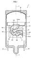
- a photomultiplier tube according to an embodiment of the present invention will be described while referring to Figs. 1 through 6.
- a photomultiplier tube 1 according to the embodiment includes a tube-shaped vacuum vessel 2 having a tube axis X.
- Fig. 1 is a cross-sectional view of the photomultiplier tube 1 cut along the tube axis X.
- the tube-shaped vacuum vessel 2 is formed of Kovar glass or a like material.
- Both ends of the tube-shaped vacuum vessel 2 along the tube axis X are closed.
- One end has a planar shape.
- a photocathode 2A is formed on the inner surface of this planar end for emitting electrons in response to incident light.
- the photocathode 2A is formed by reacting an alkali metal vapor with antimony that has been pre-deposited on the inner surface of the end.
- a plurality of lead pins 2B are provided on the other end of the tube-shaped vacuum vessel 2 for applying prescribed potentials to dynodes Dy1-Dy10 and an anode A.
- Fig. 1 shows only two of the lead pins 2B for convenience of illustration. Connecting parts not shown in the drawings serve to connect the photocathode 2A to a corresponding lead pin 2B via which a potential of -1000 V is applied.
- a cup-shaped focusing electrode 3 having a surface perpendicular to the tube axis X is disposed in a position facing the photocathode 2A.
- a center opening 3a centered at the point of intersection of the tube axis X and on a plane perpendicular thereto is formed in the focusing electrode 3.
- a mesh electrode 3A is mounted in the center opening 3a.
- the focusing electrode 3 and mesh electrode 3A are connected to corresponding lead pins 2B and have the same potential as the dynode Dy1 of the first stage.
- the dynodes Dy1-Dy10 are disposed on the opposite side of the focusing electrode 3 from the photocathode 2A for sequentially multiplying electrons.
- the dynodes Dy1-Dy10 each have secondary electron emitting surfaces.
- the dynode Dy1 of the first stage is disposed at a position facing the center opening 3a and intersecting the tube axis X.
- the dynodes Dy1-Dy10 are disposed such that the secondary electron emitting surfaces of neighboring dynodes oppose each other.
- the dynodes Dy1-Dy10 are positioned such that the paths formed between spaces of opposing dynodes continue from one to the next and intersect the tube axis X.
- the anode A is disposed on the opposite side of the tube axis X from the dynode Dy2 of the second stage. That is, as shown in Fig.
- the dynode Dy2 of the second stage is positioned on the left side of the tube axis X, while the anode A is positioned on the right.
- the mesh-shaped anode A is positioned between the dynode Dy10 of the tenth stage, serving as the final stage, and the dynode Dy9 of the ninth stage, one stage above the final stage.
- each of the dynodes Dy1-Dy10 and the anode A are connected to corresponding lead pins 2B by wires not shown in the drawings via which prescribed voltages are applied.
- the dynodes Dy2, Dy4, and Dy6-Dy9 are formed in identical shapes.
- Figs. 2(a) through 2(d) show the shape of the dynode Dy2 in more detail.
- the dynode Dy2 has a curved surface Dy2A having an arcuate cross-section and a flat surface Dy2B formed continuously and flush with the curved surface Dy2A.
- the curved surface Dy2A and flat surface Dy2B make up the secondary electron emitting surface.
- Side walls Dy2C erected from the curved surface Dy2A are formed through a pressing process on either lengthwise end of the curved surface Dy2A.
- First ear portions Dy2D forming the first support portions extend outward from both side walls Dy2C.
- Second ear portions Dy2E forming the second support portions extend outward from both lengthwise ends of the flat surface Dy2B.
- the first and second ear portions Dy2D and Dy2E are not parallel to each other but form a fixed angle. Lugs are formed in the centers of the first ear portions Dy2D and second ear portions Dy2E.
- the dynodes Dy3 and Dy5 of the third and fifth stages also have the same shape.
- Figs. 3(a) through 3(d) show the shape of the dynode Dy3 of the third stage in more detail.
- the dynode Dy3 of the third stage has a curved surface Dy3A with an arcuate cross-section.
- the curved surface Dy3A forms the secondary electron emitting surface and has a smaller surface area than the secondary electron emitting surfaces of dynodes in other stages (Dy2A + Dy2B).
- the dynode Dy3 (and dynode Dy5) is formed smaller than dynodes of other stages.
- First ear portions Dy3C are formed in a planar shape and extend outward from the side walls Dy3B perpendicular to the same on the opposite side from the curved surface Dy3A. Lugs are formed in the center portions of the first ear portions.
- side surfaces Dy1B stand upward from secondary electron emitting surfaces Dy1A on both lengthwise ends thereof, while first ear portions Dy1C extend outward from the side surfaces Dy1B. Lugs are formed in the center portions of the first ear portions Dy1C.
- the dynode Dy10 of the tenth stage has a planar secondary electron emitting surface Dy10A and two surfaces Dy10B and Dy10C standing out from both ends of the secondary electron emitting surface Dy10A.
- the dynode Dy10 of the tenth stage is formed in the shape of a three-sided rectangle.
- Three ear portions Dy10D, Dy10E, and Dy10F extend along the same plane as the secondary electron emitting surfaces Dy10A, Dy10B, and Dy10C, respectively and are formed on both lengthwise ends of the same.
- the ear portions Dy10E and Dy10F are parallel to one another, but perpendicular to the ear portions Dy10D. Lugs are formed in the center portions of the ear portions Dy10D, Dy10E, and Dy10F.
- the anode A has a secondary electron receiving portion A1 including a flat-shaped mesh construction. Ear portions A2 and A3 formed on the same plane as the receiving portion A1 extend outward from both lengthwise ends of the same.
- the dynodes Dy1-Dy10 and the anode A are supported on both lengthwise ends in base plates 4 and 5.
- Slit-shaped fixing holes Dy1c, Dy2d, Dy2e, Dy3c, Dy4d, Dy4e, Dy5c, Dy10d, Dy10e, Dy10f, a2, and a3 are formed in the base plate 5.
- identical slit-shaped fixing holes are formed in the base plate 4.
- Fig. 5 is a front view showing the dynodes Dy1-Dy10 and the anode A supported in the base plate 4 but not yet supported in the base plate 5.
- Fig. 6 shows the dynodes Dy1-Dy10 and the anode A about to be inserted into the base plate 5. The following description is identical for the case of supporting the ear portions Dy1C, Dy2D, Dy2E, Dy3C, Dy4D, Dy4E, Dy5C, Dy10D, Dy10E, and Dy10F of the dynodes Dy1-Dy10 and the anode A in the base plate 4.
- the dynode Dy1 of the first stage is supported in the base plate 5 by inserting the first ear portions Dy1C into the fixing holes Dy1c.
- the dynode Dy2 of the second stage is supported in the base plate 5 by inserting the first ear portions Dy2D into the fixing holes Dy2d and the second ear portions Dy2E into the fixing holes Dy2e.
- the dynode Dy3 of the third stage is supported in the base plate 5 by inserting the first ear portions Dy3C into the fixing holes Dy3c.
- the dynode Dy4 of the fourth stage is supported in the base plate 5 by inserting the ear portions Dy4D into the fixing holes Dy4d and the ear portions Dy4E into the fixing holes Dy4e.
- the dynode Dy5 of the fifth stage is supported in the base plate 5 by inserting the ear portions Dy5C into the fixing holes Dy5c.
- the dynodes Dy6-Dy9 are supported in the base plate 5 by inserting the first ear portions and second ear portions into the corresponding fixing holes.
- the dynode Dy10 of the tenth stage is supported in the base plate 5 by inserting the ear portions Dy10D into the fixing holes Dy10d, the ear portions Dy10E into the fixing holes Dy10e, and the ear portions Dy10F into the fixing holes Dy10f.
- the anode A is supported in the base plate 5 by inserting the ear portions A2 into the fixing holes a2 and the ear portions A3 into the fixing holes a3.
- the ear portions can be force-fitted into their corresponding fixing holes at this time.
- the dynodes Dy1-Dy10 are suitably fixed in the base plate 5. The same is true for the ear portions of the dynodes Dy6-Dy10 of the sixth through ninth stages.
- the first ear portions Dy1C, Dy2D, Dy3C, Dy4D, and Dy5C, and the ear portions Dy10E, Dy10F, A2, and A3 are formed longer than the thickness of the base plate 5, thereby protruding from the other side of the base plate 5.
- These ear portions serve as terminals for connecting to the lead pins 2B.
- the same is true for the first ear portions in the dynodes Dy6-Dy9 of the sixth through ninth stages.
- the dynodes Dy1 through Dy5 and Dy10 and the anode A can be more securely fixed to the base plate 5.
- the same effect is true for the dynodes Dy6-Dy9 of the sixth through ninth stages.
- the second ear portions Dy2E and Dy4E and the ear portion Dy10D are each formed shorter than the thickness of the base plate 5. These ear portions do not protrude from the outer side of the base plate 5 and therefore do not interfere with the wiring.
- the same description is true for the second ear portions on the dynodes Dy6-Dy9 of the sixth through ninth stages. Since the number of ear portions protruding from the base plate 5 can be decreased in this way, it is possible to avoid putting wiring of neighboring ear portions on dynodes Dy1-Dy10 in close proximity of one another, thereby preventing the problem of voltage proof destruction.
- the dynode Dy(i+2) of the (i+2) th stage is configured to penetrate between the secondary electron emitting surface of the dynodes Dyi and Dy(i+1) of the i th and (i+1) th stages, respectively.
- the dynodes Dy1-Dy10 are arranged in a curving series in order that the path formed in the spaces between dynodes cuts across the tube axis. Accordingly, a greater distance is formed between dynodes arranged on the outer part of the curve. Consequentially, the dynode Dy(i+2) of the (i+2) th stage positioned on the outer side of the curve generally does not penetrate between the secondary electron emitting surfaces of the dynodes Dyi and Dy(i+1) of the i th and (i+1) th stages.
- the secondary electron emitting surfaces of the dynodes Dy2, Dy4, Dy6, and Dy8 of the second, fourth, sixth, and eighth stages disposed on the outer part of the curve in the present embodiment are formed continuously with the curved surfaces Dy2A, Dy4A, Dy6A, and Dy8A having an arcuate cross-section. Therefore, as shown in Fig. 1, the dynode Dy(i+2) of the (i+2) th stage penetrates between the secondary electron emitting surfaces of the dynodes Dyi and Dy(i+1) of the i th and (i+1) th stages.
- the potential of the dynode Dy(i+2) of the (i+2) th stage leaks between the dynodes Dyi and Dy(i+1) of the i th and (i+1) th stages.
- secondary electrons emitted from the secondary electron emitting surface of the dynode Dyi of the i th stage are attracted to the dynode Dy(i+2) of the (i+2) th stage, enabling secondary electrons to be impinged on the part of high efficiency in the secondary electron emitting surface of the Dy(i+1) of the (i+1) th stage.
- the secondary electron emitting surfaces of the dynodes Dy3 and Dy5 of the third and fifth stages are formed only by the parts having an arcuate cross-section in order to facilitate reception of electrons from the dynodes Dy2 and Dy4 of the previous stages. Moreover, the secondary electron emitting surfaces are adjusted to emit electrons in a direction slightly toward the dynodes Dy2 and Dy4 of the previous stages so that the secondary electrons trace a correct trajectory in relation to the dynodes Dy4 and Dy6 of the next stages.
- Electrons emitted from the secondary electron emitting surfaces of the dynodes Dy2 and Dy4 would be attracted to the potential of the dynodes Dy5 and Dy7. Accordingly, the electrons would either not impinge at a desirable position on the dynodes Dy3 and Dy5 or would slip past the next stages of dynodes and impinge on the back surfaces of the dynodes Dy5 and Dy7.
- the secondary electron emitting surfaces of the dynodes Dy3 and Dy5 of the third and fifth stages have a smaller surface area than the secondary electron emitting surfaces of the dynodes Dy2, Dy4, and Dy6 through Dy9 of the second, fourth, and sixth through ninth stages in order to reduce the size of the dynodes Dy3 and Dy5 of the third and fifth stages arranged in the center of the curved series of dynodes.
- the dynodes Dy1-Dy10 can be arranged in a curved series such that the path in the spaces between dynodes crosses the tube axis.
- the secondary electron emitting surfaces of the dynodes Dy7 and Dy9 of the seventh and ninth stages arranged on the inner side of the curved series have the same surface area as the secondary electron emitting surfaces of the dynodes Dy2, Dy4, Dy6, and Dy8 of the second, fourth, sixth, and eighth stages arranged on the outer side of the curved series in order to slightly relax the increasing density of electrons near the secondary electron emitting surfaces of the dynodes Dy7 and Dy9 positioned relatively close to the final stage.
- a flat shielding plate 6 is provided parallel to the photocathode 2A and positioned around the dynodes Dy1-Dy10.
- the shielding plate 6 is positioned between the dynodes Dy7-Dy10 near the final stage and the dynode Dy1 of the first stage to prevent light or ions generated when electrons collide with the dynodes Dy7-Dy10 near the final stage from migrating toward the photocathode 2A.
- a prescribed voltage is applied to the shielding plate 6 by connecting the shielding plate 6 to a corresponding lead pin 2B.
- the operations of the photomultiplier tube 1 according to the embodiment will be described with reference to Fig. 1.
- photoelectrons are emitted.
- the photoelectrons are converged by the focusing electrode 3 and transferred to the dynode Dy1 of the first stage.
- secondary electrons are emitted from the dynode Dy1 and sequentially transmitted to the dynodes Dy2 through Dy10 of the second through tenth stages, causing an amplification cascade of sequentially generated secondary electrons.
- the secondary electrons are collected in the anode A and extracted therefrom as an output signal.
- the photomultiplier tube according to the present invention is not limited to the embodiment described above, but may be subjected to many modifications and variations without departing from the spirit of the invention, the scope of which is defined by the attached claims.
- line focus dynodes of a plurality of stages are positioned such that a curved path is formed by the spaces therebetween.
- the present invention also applies when line focus dynodes of a plurality of stages are arranged in a normal inline formation.
- the present invention described above can be applied to a wide range of applications requiring high precision optical detection and requiring good vibration resistance, as in oil exploration and the like, and good pulse linearity characteristics.
Landscapes
- Measurement Of Radiation (AREA)
- Electron Tubes For Measurement (AREA)
Abstract
Description
Claims (5)
- A photomultiplier tube comprising:characterized in that at least one dynode from among the plurality of dynodes (Dy1-Dy10) includes planar first support portions (Dy2D, Dy4D) extending outward from both ends of the secondary electron emitting surface on a base plate side and planar second support portions (Dy2E, Dy4E) also extending outward from both ends of the secondary electron emitting surface on the base plate side and forming a prescribed angle with the first support portions; anda tube-shaped vacuum vessel (2) extending along a tube axis (X);a photocathode (2A) positioned on one end of the tube-shaped vacuum vessel (2) in the tube axis, for converting incident light to electrons and emitting the electrons;a pair of electrically insulating base plates (4, 5);a plurality of dynodes arranged in stages (Dy1-Dy10) and supported between the pair of electrically insulating base plates (4, 5) and having secondary electron emitting surfaces formed on inner walls for multiplying electrons sequentially; andan anode (A) for receiving the electrons multiplied by the plurality of dynodes (Dy1-Dy10);
that the pair of electrically insulating base plates (4, 5) is formed with first through-holes (Dy2d, Dy4d) for inserting the first support portions (Dy2D, Dy4D) and second through-holes (Dy2e, Dy4e) for inserting the second support portions (Dy2E, Dy4E). - The photomultiplier tube as recited in claim 1, characterized in that the second support portions (Dy2E, Dy4E) are formed shorter than a thickness of the pair of electrically insulating base plates (4, 5) so as not to protrude from outer surfaces of the pair of electrically insulating base plates (4, 5).
- The photomultiplier tube as recited in claim 1 or 2, characterized in that the at least one dynode is formed on both ends of the secondary electron emitting surface with side walls (Dy2C) that are perpendicular to the secondary electron emitting surface, and the first support portions (Dy2D) are formed on top of the side walls (Dy2C).
- The photomultiplier tube as recited in claim 1, characterized in that lugs are formed in an approximate central position on the first support portions (Dy2D) or second support portions (Dy2E) in the thickness dimension thereof.
- The photomultiplier tube as recited in claim 1. characterized in that a shielding plate (6) is disposed between a first stage dynode (Dy1) and (n-3)th through nth stage dynodes (Dy7-Dy10) of the plurality of dynodes.
Applications Claiming Priority (3)
| Application Number | Priority Date | Filing Date | Title |
|---|---|---|---|
| JP2000227383A JP4573407B2 (en) | 2000-07-27 | 2000-07-27 | Photomultiplier tube |
| JP2000227383 | 2000-07-27 | ||
| PCT/JP2001/006281 WO2002011180A1 (en) | 2000-07-27 | 2001-07-19 | Photomultiplier |
Publications (3)
| Publication Number | Publication Date |
|---|---|
| EP1329939A1 true EP1329939A1 (en) | 2003-07-23 |
| EP1329939A4 EP1329939A4 (en) | 2005-01-19 |
| EP1329939B1 EP1329939B1 (en) | 2008-04-09 |
Family
ID=18720844
Family Applications (1)
| Application Number | Title | Priority Date | Filing Date |
|---|---|---|---|
| EP01951938A Expired - Lifetime EP1329939B1 (en) | 2000-07-27 | 2001-07-19 | Photomultiplier |
Country Status (6)
| Country | Link |
|---|---|
| US (1) | US6927538B2 (en) |
| EP (1) | EP1329939B1 (en) |
| JP (1) | JP4573407B2 (en) |
| CN (1) | CN1269179C (en) |
| AU (1) | AU2001272764A1 (en) |
| WO (1) | WO2002011180A1 (en) |
Cited By (1)
| Publication number | Priority date | Publication date | Assignee | Title |
|---|---|---|---|---|
| US7492097B2 (en) | 2005-01-25 | 2009-02-17 | Hamamatsu Photonics K.K. | Electron multiplier unit including first and second support members and photomultiplier including the same |
Families Citing this family (16)
| Publication number | Priority date | Publication date | Assignee | Title |
|---|---|---|---|---|
| US7317283B2 (en) * | 2005-03-31 | 2008-01-08 | Hamamatsu Photonics K.K. | Photomultiplier |
| US7498741B2 (en) * | 2005-03-31 | 2009-03-03 | Hamamatsu Photonics K.K. | Photomultiplier including a seated container, photocathode, and a dynode unit |
| US7397184B2 (en) * | 2005-03-31 | 2008-07-08 | Hamamatsu Photonics K.K. | Photomultiplier |
| JP4711420B2 (en) * | 2006-02-28 | 2011-06-29 | 浜松ホトニクス株式会社 | Photomultiplier tube and radiation detector |
| JP4804172B2 (en) | 2006-02-28 | 2011-11-02 | 浜松ホトニクス株式会社 | Photomultiplier tube, radiation detector, and method for manufacturing photomultiplier tube |
| JP4849521B2 (en) * | 2006-02-28 | 2012-01-11 | 浜松ホトニクス株式会社 | Photomultiplier tube and radiation detector |
| JP4804173B2 (en) * | 2006-02-28 | 2011-11-02 | 浜松ホトニクス株式会社 | Photomultiplier tube and radiation detector |
| CN101421816A (en) * | 2006-04-14 | 2009-04-29 | 浜松光子学株式会社 | Photoelectron multiplier tube |
| US7659666B2 (en) * | 2006-10-16 | 2010-02-09 | Hamamatsu Photonics K.K. | Photomultiplier |
| US7449834B2 (en) * | 2006-10-16 | 2008-11-11 | Hamamatsu Photonics K.K. | Photomultiplier having multiple dynode arrays with corresponding insulating support member |
| US7990064B2 (en) * | 2006-10-16 | 2011-08-02 | Hamamatsu Photonics K.K. | Photomultiplier |
| US7821203B2 (en) * | 2006-10-16 | 2010-10-26 | Hamamatsu Photonics K.K. | Photomultiplier |
| US9184034B2 (en) * | 2012-03-19 | 2015-11-10 | Kla-Tencor Corporation | Photomultiplier tube with extended dynamic range |
| CN203812851U (en) | 2013-12-27 | 2014-09-03 | 浜松光子学株式会社 | Photomultiplier and sensor module comprising the same |
| CN104362058A (en) * | 2014-10-15 | 2015-02-18 | 兰州空间技术物理研究所 | Curved surface film forming method for dynode of electron multiplier |
| JP7362477B2 (en) | 2019-12-27 | 2023-10-17 | 浜松ホトニクス株式会社 | Electron multiplier and photomultiplier including the same |
Family Cites Families (21)
| Publication number | Priority date | Publication date | Assignee | Title |
|---|---|---|---|---|
| DE1464358A1 (en) * | 1963-12-20 | 1969-05-08 | Philips Patentverwaltung | Electron tubes |
| JPS528377Y1 (en) * | 1969-10-06 | 1977-02-22 | ||
| FR2466851A1 (en) * | 1979-10-03 | 1981-04-10 | Labo Electronique Physique | SECONDARY EMISSION ELECTRODE, IN PARTICULAR FOR A PHOTOMULTIPLIER |
| JPS6122358Y2 (en) * | 1980-12-08 | 1986-07-04 | ||
| JPS5798056A (en) | 1980-12-11 | 1982-06-18 | Mitsubishi Electric Corp | Device for measuring ratio of operation of electronic computer for control |
| US4431943A (en) * | 1980-12-16 | 1984-02-14 | Rca Corporation | Electron discharge device having a high speed cage |
| US4439712A (en) * | 1981-08-26 | 1984-03-27 | Rca Corporation | Anode structure for photomultiplier tube |
| US4415832A (en) * | 1981-11-20 | 1983-11-15 | Rca Corporation | Electron multiplier having an improved planar utlimate dynode and planar anode structure for a photomultiplier tube |
| US4570102A (en) * | 1984-05-18 | 1986-02-11 | Rca Corporation | Photomultiplier tube having an electron multiplier cage assembly with uniform transverse spacing |
| JPS63174255A (en) * | 1987-01-12 | 1988-07-18 | Hamamatsu Photonics Kk | Photoelectron multiplier tube |
| JP2628183B2 (en) * | 1988-04-18 | 1997-07-09 | 浜松ホトニクス株式会社 | Photomultiplier tube |
| JP3267644B2 (en) * | 1991-10-24 | 2002-03-18 | 浜松ホトニクス株式会社 | Photomultiplier tube |
| JP2634353B2 (en) * | 1992-05-20 | 1997-07-23 | 浜松ホトニクス株式会社 | Electron multiplier |
| US5561347A (en) * | 1993-05-27 | 1996-10-01 | Hamamatsu Photonics K.K. | Photomultiplier |
| JPH07245078A (en) * | 1994-03-07 | 1995-09-19 | Hamamatsu Photonics Kk | Photomultiplier tube |
| JP3748608B2 (en) * | 1995-12-26 | 2006-02-22 | 浜松ホトニクス株式会社 | Photomultiplier tube |
| JPH10214588A (en) * | 1997-01-29 | 1998-08-11 | Hamamatsu Photonics Kk | Electron multiplier |
| US5914561A (en) * | 1997-08-21 | 1999-06-22 | Burle Technologies, Inc. | Shortened profile photomultiplier tube with focusing electrode |
| JP2000136795A (en) * | 1998-11-04 | 2000-05-16 | Matsushita Electric Ind Co Ltd | Electric blower and vacuum cleaner |
| JP4640881B2 (en) * | 2000-07-27 | 2011-03-02 | 浜松ホトニクス株式会社 | Photomultiplier tube |
| JP4549497B2 (en) * | 2000-07-27 | 2010-09-22 | 浜松ホトニクス株式会社 | Photomultiplier tube |
-
2000
- 2000-07-27 JP JP2000227383A patent/JP4573407B2/en not_active Expired - Lifetime
-
2001
- 2001-07-19 EP EP01951938A patent/EP1329939B1/en not_active Expired - Lifetime
- 2001-07-19 AU AU2001272764A patent/AU2001272764A1/en not_active Abandoned
- 2001-07-19 WO PCT/JP2001/006281 patent/WO2002011180A1/en not_active Ceased
- 2001-07-19 CN CNB018133266A patent/CN1269179C/en not_active Expired - Lifetime
- 2001-07-19 US US10/333,580 patent/US6927538B2/en not_active Expired - Lifetime
Cited By (2)
| Publication number | Priority date | Publication date | Assignee | Title |
|---|---|---|---|---|
| US7492097B2 (en) | 2005-01-25 | 2009-02-17 | Hamamatsu Photonics K.K. | Electron multiplier unit including first and second support members and photomultiplier including the same |
| US7495392B2 (en) | 2005-01-25 | 2009-02-24 | Hamamatsu Photonics K.K. | Electron multiplier unit including first and second support members and photomultiplier including the same |
Also Published As
| Publication number | Publication date |
|---|---|
| CN1444769A (en) | 2003-09-24 |
| EP1329939A4 (en) | 2005-01-19 |
| CN1269179C (en) | 2006-08-09 |
| WO2002011180A1 (en) | 2002-02-07 |
| JP4573407B2 (en) | 2010-11-04 |
| US6927538B2 (en) | 2005-08-09 |
| US20030122483A1 (en) | 2003-07-03 |
| JP2002042720A (en) | 2002-02-08 |
| EP1329939B1 (en) | 2008-04-09 |
| AU2001272764A1 (en) | 2002-02-13 |
Similar Documents
| Publication | Publication Date | Title |
|---|---|---|
| EP1329939B1 (en) | Photomultiplier | |
| EP1313133B1 (en) | Photomultiplier | |
| US5936348A (en) | Photomultiplier tube with focusing electrode plate | |
| US5744908A (en) | Electron tube | |
| EP1995760B1 (en) | Photomultiplier and radiation sensor | |
| EP0671757B1 (en) | Photomultiplier | |
| EP1998357B1 (en) | Photomultiplier and radiation sensor | |
| EP1995761B1 (en) | Photomultiplier and radiation detecting apparatus | |
| EP1318540B1 (en) | Photomultiplier | |
| EP1995762B1 (en) | Photomultiplier and radiation detecting apparatus | |
| US4577137A (en) | Electrode structure for an electron multiplier cage assembly | |
| US5914561A (en) | Shortened profile photomultiplier tube with focusing electrode | |
| JP4173134B2 (en) | Photomultiplier tube and method of using the same | |
| US4570102A (en) | Photomultiplier tube having an electron multiplier cage assembly with uniform transverse spacing | |
| EP0911865B1 (en) | An electron multiplier | |
| JPH0650616B2 (en) | Photomultiplier tube | |
| US4079282A (en) | Phototube having apertured electrode recessed in cup-shaped electrode |
Legal Events
| Date | Code | Title | Description |
|---|---|---|---|
| PUAI | Public reference made under article 153(3) epc to a published international application that has entered the european phase |
Free format text: ORIGINAL CODE: 0009012 |
|
| 17P | Request for examination filed |
Effective date: 20030221 |
|
| AK | Designated contracting states |
Designated state(s): AT BE CH CY DE DK ES FI FR GB GR IE IT LI LU MC NL PT SE TR |
|
| AX | Request for extension of the european patent |
Extension state: AL LT LV MK RO SI |
|
| RBV | Designated contracting states (corrected) |
Designated state(s): AT BE FR GB |
|
| REG | Reference to a national code |
Ref country code: DE Ref legal event code: 8566 |
|
| A4 | Supplementary search report drawn up and despatched |
Effective date: 20041202 |
|
| 17Q | First examination report despatched |
Effective date: 20050210 |
|
| GRAP | Despatch of communication of intention to grant a patent |
Free format text: ORIGINAL CODE: EPIDOSNIGR1 |
|
| GRAS | Grant fee paid |
Free format text: ORIGINAL CODE: EPIDOSNIGR3 |
|
| GRAC | Information related to communication of intention to grant a patent modified |
Free format text: ORIGINAL CODE: EPIDOSCIGR1 |
|
| GRAA | (expected) grant |
Free format text: ORIGINAL CODE: 0009210 |
|
| AK | Designated contracting states |
Kind code of ref document: B1 Designated state(s): FR GB |
|
| RBV | Designated contracting states (corrected) |
Designated state(s): FR GB |
|
| REG | Reference to a national code |
Ref country code: GB Ref legal event code: FG4D |
|
| ET | Fr: translation filed | ||
| PLBE | No opposition filed within time limit |
Free format text: ORIGINAL CODE: 0009261 |
|
| STAA | Information on the status of an ep patent application or granted ep patent |
Free format text: STATUS: NO OPPOSITION FILED WITHIN TIME LIMIT |
|
| 26N | No opposition filed |
Effective date: 20090112 |
|
| PGFP | Annual fee paid to national office [announced via postgrant information from national office to epo] |
Ref country code: FR Payment date: 20120719 Year of fee payment: 12 |
|
| REG | Reference to a national code |
Ref country code: FR Ref legal event code: ST Effective date: 20140331 |
|
| PG25 | Lapsed in a contracting state [announced via postgrant information from national office to epo] |
Ref country code: FR Free format text: LAPSE BECAUSE OF NON-PAYMENT OF DUE FEES Effective date: 20130731 |
|
| PGFP | Annual fee paid to national office [announced via postgrant information from national office to epo] |
Ref country code: GB Payment date: 20200708 Year of fee payment: 20 |
|
| REG | Reference to a national code |
Ref country code: GB Ref legal event code: PE20 Expiry date: 20210718 |
|
| PG25 | Lapsed in a contracting state [announced via postgrant information from national office to epo] |
Ref country code: GB Free format text: LAPSE BECAUSE OF EXPIRATION OF PROTECTION Effective date: 20210718 |