EP1329753A1 - Opto-electronic module with insulated connector - Google Patents
Opto-electronic module with insulated connector Download PDFInfo
- Publication number
- EP1329753A1 EP1329753A1 EP02250413A EP02250413A EP1329753A1 EP 1329753 A1 EP1329753 A1 EP 1329753A1 EP 02250413 A EP02250413 A EP 02250413A EP 02250413 A EP02250413 A EP 02250413A EP 1329753 A1 EP1329753 A1 EP 1329753A1
- Authority
- EP
- European Patent Office
- Prior art keywords
- receptacle
- package
- optical
- sub assembly
- nose
- Prior art date
- Legal status (The legal status is an assumption and is not a legal conclusion. Google has not performed a legal analysis and makes no representation as to the accuracy of the status listed.)
- Withdrawn
Links
Images


Classifications
-
- G—PHYSICS
- G02—OPTICS
- G02B—OPTICAL ELEMENTS, SYSTEMS OR APPARATUS
- G02B6/00—Light guides; Structural details of arrangements comprising light guides and other optical elements, e.g. couplings
- G02B6/24—Coupling light guides
- G02B6/42—Coupling light guides with opto-electronic elements
- G02B6/4201—Packages, e.g. shape, construction, internal or external details
- G02B6/4248—Feed-through connections for the hermetical passage of fibres through a package wall
-
- G—PHYSICS
- G02—OPTICS
- G02B—OPTICAL ELEMENTS, SYSTEMS OR APPARATUS
- G02B6/00—Light guides; Structural details of arrangements comprising light guides and other optical elements, e.g. couplings
- G02B6/24—Coupling light guides
- G02B6/42—Coupling light guides with opto-electronic elements
- G02B6/4201—Packages, e.g. shape, construction, internal or external details
- G02B6/4204—Packages, e.g. shape, construction, internal or external details the coupling comprising intermediate optical elements, e.g. lenses, holograms
- G02B6/421—Packages, e.g. shape, construction, internal or external details the coupling comprising intermediate optical elements, e.g. lenses, holograms the intermediate optical component consisting of a short length of fibre, e.g. fibre stub
-
- G—PHYSICS
- G02—OPTICS
- G02B—OPTICAL ELEMENTS, SYSTEMS OR APPARATUS
- G02B6/00—Light guides; Structural details of arrangements comprising light guides and other optical elements, e.g. couplings
- G02B6/24—Coupling light guides
- G02B6/42—Coupling light guides with opto-electronic elements
- G02B6/4201—Packages, e.g. shape, construction, internal or external details
- G02B6/4246—Bidirectionally operating package structures
-
- G—PHYSICS
- G02—OPTICS
- G02B—OPTICAL ELEMENTS, SYSTEMS OR APPARATUS
- G02B6/00—Light guides; Structural details of arrangements comprising light guides and other optical elements, e.g. couplings
- G02B6/24—Coupling light guides
- G02B6/42—Coupling light guides with opto-electronic elements
- G02B6/4201—Packages, e.g. shape, construction, internal or external details
- G02B6/4274—Electrical aspects
- G02B6/4277—Protection against electromagnetic interference [EMI], e.g. shielding means
-
- G—PHYSICS
- G02—OPTICS
- G02B—OPTICAL ELEMENTS, SYSTEMS OR APPARATUS
- G02B6/00—Light guides; Structural details of arrangements comprising light guides and other optical elements, e.g. couplings
- G02B6/24—Coupling light guides
- G02B6/42—Coupling light guides with opto-electronic elements
- G02B6/4292—Coupling light guides with opto-electronic elements the light guide being disconnectable from the opto-electronic element, e.g. mutually self aligning arrangements
-
- G—PHYSICS
- G02—OPTICS
- G02B—OPTICAL ELEMENTS, SYSTEMS OR APPARATUS
- G02B6/00—Light guides; Structural details of arrangements comprising light guides and other optical elements, e.g. couplings
- G02B6/24—Coupling light guides
- G02B6/42—Coupling light guides with opto-electronic elements
- G02B6/4201—Packages, e.g. shape, construction, internal or external details
- G02B6/4204—Packages, e.g. shape, construction, internal or external details the coupling comprising intermediate optical elements, e.g. lenses, holograms
-
- G—PHYSICS
- G02—OPTICS
- G02B—OPTICAL ELEMENTS, SYSTEMS OR APPARATUS
- G02B6/00—Light guides; Structural details of arrangements comprising light guides and other optical elements, e.g. couplings
- G02B6/24—Coupling light guides
- G02B6/42—Coupling light guides with opto-electronic elements
- G02B6/4201—Packages, e.g. shape, construction, internal or external details
- G02B6/4219—Mechanical fixtures for holding or positioning the elements relative to each other in the couplings; Alignment methods for the elements, e.g. measuring or observing methods especially used therefor
- G02B6/422—Active alignment, i.e. moving the elements in response to the detected degree of coupling or position of the elements
- G02B6/4225—Active alignment, i.e. moving the elements in response to the detected degree of coupling or position of the elements by a direct measurement of the degree of coupling, e.g. the amount of light power coupled to the fibre or the opto-electronic element
-
- G—PHYSICS
- G02—OPTICS
- G02B—OPTICAL ELEMENTS, SYSTEMS OR APPARATUS
- G02B6/00—Light guides; Structural details of arrangements comprising light guides and other optical elements, e.g. couplings
- G02B6/24—Coupling light guides
- G02B6/42—Coupling light guides with opto-electronic elements
- G02B6/4201—Packages, e.g. shape, construction, internal or external details
- G02B6/4219—Mechanical fixtures for holding or positioning the elements relative to each other in the couplings; Alignment methods for the elements, e.g. measuring or observing methods especially used therefor
- G02B6/4236—Fixing or mounting methods of the aligned elements
Definitions
- This invention relates to an optical sub assembly for receiving an optical fibre transmission line for coupling to an optical device and to a receptacle for use in such a sub assembly.
- this invention relates to an optical sub assembly for coupling via a receptacle which is able to provide electrical isolation between the receptacle for receiving the optical fibre and a package housing the optical device.
- the invention also extends to a method of manufacturing such an optical sub assembly.
- a transmitter or receiver component are mounted in a metal panel.
- a receptacle which may extend outwardly through an aperture in the panel is provided for receiving an optical fibre, and a package extending behind the panel houses the transmitter or the receiver.
- the receptacle houses a ceramic ferrule containing an optical fibre stub and a package has an aperture for receiving the ceramic ferrule.
- the receptacle and the package may be aligned to obtain an optimum coupling efficiency between the fibre stub and the optical device.
- the receptacle is secured to the package by soldering, welding or brazing.
- the receptacle and the package are formed from a stable material such as stainless steel.
- the panel is earthed (grounded) through the mains, which results in the package housing the optical device being earthed through the mains.
- the transmitter and receiver operate at very high frequencies (GHz) and they are supplied with electrical power at low voltages from stabilised power supplies.
- GHz frequency
- These power supplies are generally earthed independently of the casing, which means that the earth on the housing of the optical devices is not the same earth as the earth on the electronic circuit boards upon which the optical devices are mounted.
- an optical fibre receptacle for receiving an optical fibre transmission line comprising a nose housing an end of an insulating ferrule, and having an aperture for receiving said optical fibre transmission line; characterised in that the receptacle further comprises a sleeve extending along a second portion of the ferrule; and an insulating disc positioned between the sleeve and the nose providing, along with the insulating ferrule, electrical insulation between the sleeve and the nose.
- an optical sub assembly comprising a receptacle as described above; a package having an aperture at one end for receiving the receptacle and an optical device housed within the package.
- the receptacle are connected together using an electrically conducting hermetic seal which may be achieved by welding, soldering or brazing.
- an optical fibre sub assembly comprising the steps of actively aligning a receptacle as described previously with an optical device positioned within a package, when an optimum coupling efficiency is achieved, securing the receptacle to the rear part.
- an optical sub assembly comprises a receptacle 1 for receiving an optical fibre, and a package 2 housing an optical device 3.
- the optical device is an optical transmitter, which is coupled to an optical fibre stub in a ceramic ferrule 10 by a lens 5.
- the optical device 3 is mounted on a circuit board 4.
- two such sub assemblies housing an optical transmitter and an optical receiver will be mounted in a metal box, and mounted on a metal plate as a transceiver pair, possibly alongside several other transceiver pairs.
- RF emissions are generated by the optical components, and the package casing is electrically noisy. Hence there is a requirement to electrically isolate the receptacle from the package.
- the receptacle 1 comprises a nose 8, which is generally cylindrical in shape, having an aperture 9 at one end for receiving an optical fibre.
- the nose has a chamfered edge at the end with the aperture.
- the other end of the nose houses the ceramic ferrule 10 which is arranged to hold an optical fibre stub.
- the ceramic ferrule 10 has a split sleeve 11 fitted around one end, which is arranged to centre and clamp the end of the ferrule 10.
- the nose 8 and the split sleeve 11 are fitted to a holder 14.
- This embodiment of the invention has a ceramic ferrule, but it will be understood that any suitable electrically insulating material may be used.
- a ceramic washer 15 is positioned between a sleeve 12 and the holder 14.
- the ceramic washer 15 has the front and back faces plated with an appropriate metal in order to allow soldering or brazing of the washer to the holder 14 and to the sleeve 12.
- the ceramic washer 15, together with the ceramic ferrule 10 electrically isolates the two parts of the sub assembly from each other so that the package housing the optical device can be earthed to a different earth than the receptacle of the sub assembly into which a user inserts an optical fibre transmission line.
- an alignment collar 6 attached to the exterior of the package 2.
- the alignment collar 6 allows the receptacle 1, containing an optical fibre stub, to be actively aligned with the optical transmitter 3.
- Active alignment is the process of alignment that is carried out with the optical transmitter 3 switched on.
- the coupling efficiency achieved between the optical transmitter 3 and the optical fibre stub, is measured.
- the receptacle 1 is considered to be optimally aligned with the optical transmitter 3.
- the receptacle is brazed, soldered or welded to the alignment collar, achieving a hermetic seal whilst allowing the receptacle to be electrically isolated from the package.
- Figure 3 illustrates a second embodiment of the invention, in which the sub assembly is designed to connect an optical fibre (not shown) to an optical receiver 3'.
- the sub assembly is designed to connect an optical fibre (not shown) to an optical receiver 3'.
- Figure 4 illustrates a cross section of the sub assembly shown in Figure 3.
- the receptacle 1 and the package 2 are similar to those illustrated in Figure 2, although the alignment collar 12 of Figure 2 has been omitted in the embodiment shown in Figure 4.
Landscapes
- Physics & Mathematics (AREA)
- General Physics & Mathematics (AREA)
- Optics & Photonics (AREA)
- Electromagnetism (AREA)
- Optical Couplings Of Light Guides (AREA)
Abstract
This invention relates to an optical sub assembly for
receiving an optical fibre transmission line for coupling
to an optical device, to a receptacle for use in such a
sub assembly and to a method of manufacture of such a sub
assembly. In particular, this invention relates to an
optical sub assembly which provides electrical isolation
between a receptacle (1) having a nose (8) for receiving
the optical fibre and a package (2) housing an optical
device (3).
The nose (8) houses a ferrule (10) containing a fibre stub
(13) which may be optically aligned with an optical device
(3) housed in a package (2) before securing the
receptacle (1) to the package (2). In this invention
electrical insulation is provided between the nose (8) and
the package (2) by means of a sleeve (12) extending along
a middle portion of the ferrule (10) and an insulating
portion (15) positioned between the sleeve (12) and the
nose (8).
Description
- This invention relates to an optical sub assembly for receiving an optical fibre transmission line for coupling to an optical device and to a receptacle for use in such a sub assembly. In particular, this invention relates to an optical sub assembly for coupling via a receptacle which is able to provide electrical isolation between the receptacle for receiving the optical fibre and a package housing the optical device. The invention also extends to a method of manufacturing such an optical sub assembly.
- Typically a transmitter or receiver component are mounted in a metal panel. A receptacle which may extend outwardly through an aperture in the panel is provided for receiving an optical fibre, and a package extending behind the panel houses the transmitter or the receiver. In known optical sub assemblies the receptacle houses a ceramic ferrule containing an optical fibre stub and a package has an aperture for receiving the ceramic ferrule. The receptacle and the package may be aligned to obtain an optimum coupling efficiency between the fibre stub and the optical device. The receptacle is secured to the package by soldering, welding or brazing. In order to maintain dimensional stability the receptacle and the package are formed from a stable material such as stainless steel.
- In order to prevent electromagnetic emissions, the panel is earthed (grounded) through the mains, which results in the package housing the optical device being earthed through the mains. However, the transmitter and receiver operate at very high frequencies (GHz) and they are supplied with electrical power at low voltages from stabilised power supplies. These power supplies are generally earthed independently of the casing, which means that the earth on the housing of the optical devices is not the same earth as the earth on the electronic circuit boards upon which the optical devices are mounted.
- High frequency operation results in a radio frequency emission problem. One way in which the emission problem could be reduced would be to provide the same earth for the power supply and the mounting panel. However this is counter to the user requirement for freedom to have a different earth for the power supply and the mounting panel, so the problem to be solved is to provide an optical sub assembly in which the receptacle and package may be electrically isolated from one another.
- This problem is not as straightforward to solve as it might initially seem, due to the dimensional stability required for the receptacle. Furthermore, for a sub assembly for an optical transmitter there may be a requirement to align a ceramic ferrule housed in the receptacle with the optical transmitter housed in the package prior to securing the receptacle to the package. The securing process must maintain an optimum alignment within typically 0.1 - 1 µm (micron).
- According to the present invention there is provided an optical fibre receptacle for receiving an optical fibre transmission line comprising a nose housing an end of an insulating ferrule, and having an aperture for receiving said optical fibre transmission line; characterised in that the receptacle further comprises a sleeve extending along a second portion of the ferrule; and an insulating disc positioned between the sleeve and the nose providing, along with the insulating ferrule, electrical insulation between the sleeve and the nose.
- According to another aspect of the invention there is provided an optical sub assembly comprising a receptacle as described above; a package having an aperture at one end for receiving the receptacle and an optical device housed within the package.
- It is an advantage if the receptacle are connected together using an electrically conducting hermetic seal which may be achieved by welding, soldering or brazing.
- According to a further aspect of the invention there is also provided a method of manufacturing an optical fibre sub assembly comprising the steps of actively aligning a receptacle as described previously with an optical device positioned within a package, when an optimum coupling efficiency is achieved, securing the receptacle to the rear part.
- It is an advantage, in this method, if the receptacle and the package are connected together using an electrically conducting hermetic seal which may be achieved by welding, soldering or brazing.
- Embodiments of the invention will now be described, by way of example only, with reference to the accompanying drawings, in which:
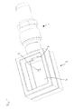
- Figure 1 shows a perspective view of an optical sub assembly according to a first embodiment of the present invention;
- Figure 2 illustrates a side cross section of the fibre sub assembly of figure 1;
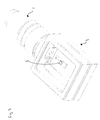
- Figure 3 shows a perspective view of an optical sub assembly according to a second embodiment of the present invention; and
- Figure 4 illustrates a side cross section of the sub assembly of figure 3.
-
- Referring firstly to figure 1, an optical sub assembly comprises a
receptacle 1 for receiving an optical fibre, and apackage 2 housing anoptical device 3. In this case the optical device is an optical transmitter, which is coupled to an optical fibre stub in aceramic ferrule 10 by a lens 5. Theoptical device 3 is mounted on acircuit board 4. Conventionally, two such sub assemblies housing an optical transmitter and an optical receiver will be mounted in a metal box, and mounted on a metal plate as a transceiver pair, possibly alongside several other transceiver pairs. RF emissions are generated by the optical components, and the package casing is electrically noisy. Hence there is a requirement to electrically isolate the receptacle from the package. - Referring now to Figure 2, the
receptacle 1 comprises anose 8, which is generally cylindrical in shape, having an aperture 9 at one end for receiving an optical fibre. The nose has a chamfered edge at the end with the aperture. The other end of the nose houses theceramic ferrule 10 which is arranged to hold an optical fibre stub. Theceramic ferrule 10 has a split sleeve 11 fitted around one end, which is arranged to centre and clamp the end of theferrule 10. Thenose 8 and the split sleeve 11 are fitted to aholder 14. This embodiment of the invention has a ceramic ferrule, but it will be understood that any suitable electrically insulating material may be used. - An insulating portion, in this case a
ceramic washer 15 is positioned between asleeve 12 and theholder 14. Theceramic washer 15 has the front and back faces plated with an appropriate metal in order to allow soldering or brazing of the washer to theholder 14 and to thesleeve 12. - The
ceramic washer 15, together with theceramic ferrule 10 electrically isolates the two parts of the sub assembly from each other so that the package housing the optical device can be earthed to a different earth than the receptacle of the sub assembly into which a user inserts an optical fibre transmission line. - It will be understood that the ceramic ferrule is likely to be extended compared to ferrules of prior art sub assemblies, due to the presence of the
sleeve 12, and thewasher 15. - In the transceiver of Figure 1 and Figure 2 there is shown an alignment collar 6 attached to the exterior of the
package 2. The alignment collar 6 allows thereceptacle 1, containing an optical fibre stub, to be actively aligned with theoptical transmitter 3. Active alignment is the process of alignment that is carried out with theoptical transmitter 3 switched on. The coupling efficiency achieved between theoptical transmitter 3 and the optical fibre stub, is measured. Once a desired coupling efficiency is achieved then thereceptacle 1 is considered to be optimally aligned with theoptical transmitter 3. Then the receptacle is brazed, soldered or welded to the alignment collar, achieving a hermetic seal whilst allowing the receptacle to be electrically isolated from the package. - Figure 3 illustrates a second embodiment of the invention, in which the sub assembly is designed to connect an optical fibre (not shown) to an optical receiver 3'. In this example there is no coupling lens used.
- Figure 4 illustrates a cross section of the sub assembly shown in Figure 3. The
receptacle 1 and thepackage 2 are similar to those illustrated in Figure 2, although thealignment collar 12 of Figure 2 has been omitted in the embodiment shown in Figure 4.
Claims (7)
- An optical fibre receptacle (1) for receiving an optical fibre transmission line comprising
a nose (8) housing an end of an insulating ferrule (10), and having an aperture (9) for receiving said optical fibre transmission line; characterised in that the receptacle further comprises
a sleeve (12) extending along a second portion of the ferrule (10); and
an insulating portion (15) positioned between the sleeve (12) and the nose (8) providing, along with the insulating ferrule (10), electrical insulation between the sleeve (12) and the nose (8). - An optical fibre sub assembly comprising
a receptacle according to claim 1;
a package (2) having an aperture at one end for receiving the receptacle (1) and
an optical device (3) housed within the package (2). - A sub assembly according to claim 2, in which the package and the receptacle are connected together using an electrically conducting hermetic seal.
- A sub assembly according to claim 3, in which the seal is provided by welding, soldering or brazing.
- A method of manufacturing an optical sub assembly comprising the steps:actively aligning a receptacle according to claim 1 with an optical device positioned within a package;when a predetermined coupling efficiency is achieved, securing the receptacle to the rear part.
- A method according to claim 5, in which the securing step comprises connecting the receptacle and the package to each other using an electrically conducting hermetically seal.
- A method according to claim 6 in which the securing step comprises connecting the receptacle and the package to each other by welding, soldering or brazing.
Priority Applications (2)
| Application Number | Priority Date | Filing Date | Title |
|---|---|---|---|
| EP02250413A EP1329753A1 (en) | 2002-01-21 | 2002-01-21 | Opto-electronic module with insulated connector |
| US10/328,207 US7261473B2 (en) | 2002-01-21 | 2002-12-23 | Optical sub assembly |
Applications Claiming Priority (1)
| Application Number | Priority Date | Filing Date | Title |
|---|---|---|---|
| EP02250413A EP1329753A1 (en) | 2002-01-21 | 2002-01-21 | Opto-electronic module with insulated connector |
Publications (1)
| Publication Number | Publication Date |
|---|---|
| EP1329753A1 true EP1329753A1 (en) | 2003-07-23 |
Family
ID=8185659
Family Applications (1)
| Application Number | Title | Priority Date | Filing Date |
|---|---|---|---|
| EP02250413A Withdrawn EP1329753A1 (en) | 2002-01-21 | 2002-01-21 | Opto-electronic module with insulated connector |
Country Status (2)
| Country | Link |
|---|---|
| US (1) | US7261473B2 (en) |
| EP (1) | EP1329753A1 (en) |
Cited By (5)
| Publication number | Priority date | Publication date | Assignee | Title |
|---|---|---|---|---|
| US6976795B2 (en) | 2002-10-10 | 2005-12-20 | Sumitomo Electric Industries, Ltd. | Optical device and optical module |
| US7090412B2 (en) | 2002-08-02 | 2006-08-15 | Sumitomo Electric Industries, Ltd. | Optical module |
| US7172348B2 (en) | 2004-04-20 | 2007-02-06 | Sumitomo Electric Industries, Ltd. | Optical sub-assembly having an enhanced discharge-resistant arrangement and an optical transceiver using the same |
| US7275877B2 (en) | 2003-04-30 | 2007-10-02 | Sumitomo Electric Industries, Ltd. | Optical module having individual housing for an optical processing unit and an optical sub-assembly |
| CN101587215A (en) * | 2008-04-24 | 2009-11-25 | 雷迪埃公司 | Mix the multiconductor joint |
Families Citing this family (9)
| Publication number | Priority date | Publication date | Assignee | Title |
|---|---|---|---|---|
| US7646988B2 (en) * | 2006-08-04 | 2010-01-12 | Finisar Corporation | Linear amplifier for use with laser driver signal |
| US20080056647A1 (en) * | 2006-08-31 | 2008-03-06 | Mark Margolin | Active modular optoelectronic components |
| US7665903B2 (en) * | 2007-10-03 | 2010-02-23 | Avago Technologies Fiber Ip (Singapore) Pte. Ltd. | Optical receptacle having an electrically isolating ring for electrically isolating the signal ground and the chassis ground in an optical transceiver module |
| US8066437B2 (en) * | 2009-03-12 | 2011-11-29 | Avago Technologies Fiber Ip (Singapore) Pte. Ltd | Optical transceiver module providing EMI shielding and electrical isolation between a signal ground and a chassis ground |
| US8582969B1 (en) | 2010-11-30 | 2013-11-12 | Adtran, Inc. | Passive optical network (PON) having optical network unit (ONU) using feedback to detect rogue conditions and related method |
| JP6628239B2 (en) * | 2015-05-28 | 2020-01-08 | 住友電工デバイス・イノベーション株式会社 | Optical module |
| JP2017003634A (en) * | 2015-06-05 | 2017-01-05 | Nttエレクトロニクス株式会社 | Optical module and optical receptacle |
| JP2019015813A (en) * | 2017-07-05 | 2019-01-31 | 住友電気工業株式会社 | Optical receptacle, fiber stub and optical module |
| US12298561B2 (en) | 2021-11-13 | 2025-05-13 | John Marmo | Re-spliceable splice-on connector and method of making same |
Citations (8)
| Publication number | Priority date | Publication date | Assignee | Title |
|---|---|---|---|---|
| US4118105A (en) * | 1975-06-23 | 1978-10-03 | Max-Planck-Gesellschft zur Forderung der Wissenschaften e.V. | Optical coupling |
| US4207587A (en) * | 1977-05-26 | 1980-06-10 | Electric Power Research Institute, Inc. | Package for light-triggered thyristor |
| JPS583281A (en) * | 1981-06-30 | 1983-01-10 | Toshiba Corp | Photovoltaic type semiconductor device |
| JPS584989A (en) * | 1981-07-01 | 1983-01-12 | Mitsubishi Rayon Co Ltd | optical coupling device |
| US4466009A (en) * | 1980-11-21 | 1984-08-14 | Hitachi, Ltd. | Light-activated semiconductor device with optic fiber moveable azimuthally and transversely |
| US5085492A (en) * | 1990-10-01 | 1992-02-04 | Iris Medical Instruments, Inc. | Optical fiber with electrical encoding |
| EP0586096A1 (en) * | 1992-08-25 | 1994-03-09 | Yamaichi Electronics Co., Ltd. | Optical connector |
| EP0918238A1 (en) * | 1997-10-23 | 1999-05-26 | Hewlett-Packard Company | Optical device for connecting a semiconductor device and a waveguide. |
Family Cites Families (5)
| Publication number | Priority date | Publication date | Assignee | Title |
|---|---|---|---|---|
| US4222629A (en) * | 1978-03-27 | 1980-09-16 | Sperry Corporation | Fiber optic connector assembly |
| US4466609A (en) * | 1982-04-19 | 1984-08-21 | Gradco Systems, Inc. | Compact sheet sorter |
| US4708429A (en) * | 1985-09-26 | 1987-11-24 | Rca Corporation | Optical fiber assembly and optically coupled device package including same |
| US5450515A (en) * | 1993-04-29 | 1995-09-12 | Cts Corporation | Detachable fiber optic connector |
| JP3934234B2 (en) * | 1998-01-21 | 2007-06-20 | 富士通株式会社 | Receptacle module |
-
2002
- 2002-01-21 EP EP02250413A patent/EP1329753A1/en not_active Withdrawn
- 2002-12-23 US US10/328,207 patent/US7261473B2/en not_active Expired - Lifetime
Patent Citations (8)
| Publication number | Priority date | Publication date | Assignee | Title |
|---|---|---|---|---|
| US4118105A (en) * | 1975-06-23 | 1978-10-03 | Max-Planck-Gesellschft zur Forderung der Wissenschaften e.V. | Optical coupling |
| US4207587A (en) * | 1977-05-26 | 1980-06-10 | Electric Power Research Institute, Inc. | Package for light-triggered thyristor |
| US4466009A (en) * | 1980-11-21 | 1984-08-14 | Hitachi, Ltd. | Light-activated semiconductor device with optic fiber moveable azimuthally and transversely |
| JPS583281A (en) * | 1981-06-30 | 1983-01-10 | Toshiba Corp | Photovoltaic type semiconductor device |
| JPS584989A (en) * | 1981-07-01 | 1983-01-12 | Mitsubishi Rayon Co Ltd | optical coupling device |
| US5085492A (en) * | 1990-10-01 | 1992-02-04 | Iris Medical Instruments, Inc. | Optical fiber with electrical encoding |
| EP0586096A1 (en) * | 1992-08-25 | 1994-03-09 | Yamaichi Electronics Co., Ltd. | Optical connector |
| EP0918238A1 (en) * | 1997-10-23 | 1999-05-26 | Hewlett-Packard Company | Optical device for connecting a semiconductor device and a waveguide. |
Non-Patent Citations (2)
| Title |
|---|
| PATENT ABSTRACTS OF JAPAN vol. 007, no. 072 (E - 166) 25 March 1983 (1983-03-25) * |
| PATENT ABSTRACTS OF JAPAN vol. 007, no. 076 (E - 167) 30 March 1983 (1983-03-30) * |
Cited By (5)
| Publication number | Priority date | Publication date | Assignee | Title |
|---|---|---|---|---|
| US7090412B2 (en) | 2002-08-02 | 2006-08-15 | Sumitomo Electric Industries, Ltd. | Optical module |
| US6976795B2 (en) | 2002-10-10 | 2005-12-20 | Sumitomo Electric Industries, Ltd. | Optical device and optical module |
| US7275877B2 (en) | 2003-04-30 | 2007-10-02 | Sumitomo Electric Industries, Ltd. | Optical module having individual housing for an optical processing unit and an optical sub-assembly |
| US7172348B2 (en) | 2004-04-20 | 2007-02-06 | Sumitomo Electric Industries, Ltd. | Optical sub-assembly having an enhanced discharge-resistant arrangement and an optical transceiver using the same |
| CN101587215A (en) * | 2008-04-24 | 2009-11-25 | 雷迪埃公司 | Mix the multiconductor joint |
Also Published As
| Publication number | Publication date |
|---|---|
| US20040022500A1 (en) | 2004-02-05 |
| US7261473B2 (en) | 2007-08-28 |
Similar Documents
| Publication | Publication Date | Title |
|---|---|---|
| US7261473B2 (en) | Optical sub assembly | |
| US11360279B2 (en) | Optical subassembly and optical module | |
| US6358066B1 (en) | Surface mountable transceiver | |
| US6874953B2 (en) | Methods and apparatus for fiber-optic modules with shielded housings/covers with fingers | |
| US6572272B2 (en) | Angled optical connector mounting assembly | |
| US6937824B2 (en) | Optical transceiver, connector, substrate unit, optical transmitter, optical receiver, and semiconductor device | |
| US20040208461A1 (en) | Transparent substrate and hinged optical assembly | |
| US7444736B1 (en) | Method for fabricating horn antenna | |
| US6824314B2 (en) | Package for opto-electrical components | |
| US20040264980A1 (en) | Optical receiver module with To-Can structure | |
| US20240345346A1 (en) | Emi shielding component, optical fiber adapter module having the same, and method of assembling the optical fiber adapter module | |
| US20020154362A1 (en) | Optical link module | |
| US20050018978A1 (en) | Opto-electric module and method of assembling | |
| JP2001345610A (en) | Dielectric resonator, filter, duplexer and communication device | |
| JP3833610B2 (en) | Power supply terminal and backboard | |
| US6824315B2 (en) | Optical module | |
| JP2003029094A (en) | Optical transmission equipment | |
| EP1217402A2 (en) | Angled optical connector mounting assembly | |
| EP1525679A1 (en) | Bias-t apparatus and center conductor of the same | |
| JP3803264B2 (en) | Optical transceiver and method for manufacturing optical transceiver | |
| CN210576557U (en) | Connector for microwave signal and power feed | |
| JPH09232789A (en) | Portable high frequency equipment | |
| JP4702029B2 (en) | Manufacturing method of coaxial optical module | |
| US20030169125A1 (en) | Transition from a coaxial transmission line to a printed circuit transmission line | |
| JPH0451475A (en) | Connector for micro strip line |
Legal Events
| Date | Code | Title | Description |
|---|---|---|---|
| PUAI | Public reference made under article 153(3) epc to a published international application that has entered the european phase |
Free format text: ORIGINAL CODE: 0009012 |
|
| AK | Designated contracting states |
Designated state(s): AT BE CH CY DE DK ES FI FR GB GR IE IT LI LU MC NL PT SE TR |
|
| AX | Request for extension of the european patent |
Extension state: AL LT LV MK RO SI |
|
| 17P | Request for examination filed |
Effective date: 20040123 |
|
| AKX | Designation fees paid |
Designated state(s): DE GB |
|
| RAP1 | Party data changed (applicant data changed or rights of an application transferred) |
Owner name: AVAGO TECHNOLOGIES FIBER IP (SINGAPORE) PTE. LTD. |
|
| STAA | Information on the status of an ep patent application or granted ep patent |
Free format text: STATUS: THE APPLICATION IS DEEMED TO BE WITHDRAWN |
|
| 18D | Application deemed to be withdrawn |
Effective date: 20091208 |