EP1327958A1 - Noncontact communication medium and noncontact communication system - Google Patents
Noncontact communication medium and noncontact communication system Download PDFInfo
- Publication number
- EP1327958A1 EP1327958A1 EP01936953A EP01936953A EP1327958A1 EP 1327958 A1 EP1327958 A1 EP 1327958A1 EP 01936953 A EP01936953 A EP 01936953A EP 01936953 A EP01936953 A EP 01936953A EP 1327958 A1 EP1327958 A1 EP 1327958A1
- Authority
- EP
- European Patent Office
- Prior art keywords
- noncontact
- output voltage
- card
- state
- resonant circuit
- Prior art date
- Legal status (The legal status is an assumption and is not a legal conclusion. Google has not performed a legal analysis and makes no representation as to the accuracy of the status listed.)
- Granted
Links
Images







Classifications
-
- G—PHYSICS
- G06—COMPUTING OR CALCULATING; COUNTING
- G06K—GRAPHICAL DATA READING; PRESENTATION OF DATA; RECORD CARRIERS; HANDLING RECORD CARRIERS
- G06K19/00—Record carriers for use with machines and with at least a part designed to carry digital markings
- G06K19/06—Record carriers for use with machines and with at least a part designed to carry digital markings characterised by the kind of the digital marking, e.g. shape, nature, code
- G06K19/067—Record carriers with conductive marks, printed circuits or semiconductor circuit elements, e.g. credit or identity cards also with resonating or responding marks without active components
- G06K19/07—Record carriers with conductive marks, printed circuits or semiconductor circuit elements, e.g. credit or identity cards also with resonating or responding marks without active components with integrated circuit chips
- G06K19/077—Constructional details, e.g. mounting of circuits in the carrier
- G06K19/07749—Constructional details, e.g. mounting of circuits in the carrier the record carrier being capable of non-contact communication, e.g. constructional details of the antenna of a non-contact smart card
- G06K19/0775—Constructional details, e.g. mounting of circuits in the carrier the record carrier being capable of non-contact communication, e.g. constructional details of the antenna of a non-contact smart card arrangements for connecting the integrated circuit to the antenna
-
- G—PHYSICS
- G06—COMPUTING OR CALCULATING; COUNTING
- G06K—GRAPHICAL DATA READING; PRESENTATION OF DATA; RECORD CARRIERS; HANDLING RECORD CARRIERS
- G06K19/00—Record carriers for use with machines and with at least a part designed to carry digital markings
- G06K19/06—Record carriers for use with machines and with at least a part designed to carry digital markings characterised by the kind of the digital marking, e.g. shape, nature, code
- G06K19/067—Record carriers with conductive marks, printed circuits or semiconductor circuit elements, e.g. credit or identity cards also with resonating or responding marks without active components
- G06K19/07—Record carriers with conductive marks, printed circuits or semiconductor circuit elements, e.g. credit or identity cards also with resonating or responding marks without active components with integrated circuit chips
- G06K19/0701—Record carriers with conductive marks, printed circuits or semiconductor circuit elements, e.g. credit or identity cards also with resonating or responding marks without active components with integrated circuit chips at least one of the integrated circuit chips comprising an arrangement for power management
-
- G—PHYSICS
- G06—COMPUTING OR CALCULATING; COUNTING
- G06K—GRAPHICAL DATA READING; PRESENTATION OF DATA; RECORD CARRIERS; HANDLING RECORD CARRIERS
- G06K19/00—Record carriers for use with machines and with at least a part designed to carry digital markings
- G06K19/06—Record carriers for use with machines and with at least a part designed to carry digital markings characterised by the kind of the digital marking, e.g. shape, nature, code
- G06K19/067—Record carriers with conductive marks, printed circuits or semiconductor circuit elements, e.g. credit or identity cards also with resonating or responding marks without active components
- G06K19/07—Record carriers with conductive marks, printed circuits or semiconductor circuit elements, e.g. credit or identity cards also with resonating or responding marks without active components with integrated circuit chips
- G06K19/0701—Record carriers with conductive marks, printed circuits or semiconductor circuit elements, e.g. credit or identity cards also with resonating or responding marks without active components with integrated circuit chips at least one of the integrated circuit chips comprising an arrangement for power management
- G06K19/0715—Record carriers with conductive marks, printed circuits or semiconductor circuit elements, e.g. credit or identity cards also with resonating or responding marks without active components with integrated circuit chips at least one of the integrated circuit chips comprising an arrangement for power management the arrangement including means to regulate power transfer to the integrated circuit
-
- G—PHYSICS
- G06—COMPUTING OR CALCULATING; COUNTING
- G06K—GRAPHICAL DATA READING; PRESENTATION OF DATA; RECORD CARRIERS; HANDLING RECORD CARRIERS
- G06K19/00—Record carriers for use with machines and with at least a part designed to carry digital markings
- G06K19/06—Record carriers for use with machines and with at least a part designed to carry digital markings characterised by the kind of the digital marking, e.g. shape, nature, code
- G06K19/067—Record carriers with conductive marks, printed circuits or semiconductor circuit elements, e.g. credit or identity cards also with resonating or responding marks without active components
- G06K19/07—Record carriers with conductive marks, printed circuits or semiconductor circuit elements, e.g. credit or identity cards also with resonating or responding marks without active components with integrated circuit chips
- G06K19/0723—Record carriers with conductive marks, printed circuits or semiconductor circuit elements, e.g. credit or identity cards also with resonating or responding marks without active components with integrated circuit chips the record carrier comprising an arrangement for non-contact communication, e.g. wireless communication circuits on transponder cards, non-contact smart cards or RFIDs
-
- G—PHYSICS
- G06—COMPUTING OR CALCULATING; COUNTING
- G06K—GRAPHICAL DATA READING; PRESENTATION OF DATA; RECORD CARRIERS; HANDLING RECORD CARRIERS
- G06K19/00—Record carriers for use with machines and with at least a part designed to carry digital markings
- G06K19/06—Record carriers for use with machines and with at least a part designed to carry digital markings characterised by the kind of the digital marking, e.g. shape, nature, code
- G06K19/067—Record carriers with conductive marks, printed circuits or semiconductor circuit elements, e.g. credit or identity cards also with resonating or responding marks without active components
- G06K19/07—Record carriers with conductive marks, printed circuits or semiconductor circuit elements, e.g. credit or identity cards also with resonating or responding marks without active components with integrated circuit chips
- G06K19/077—Constructional details, e.g. mounting of circuits in the carrier
- G06K19/07749—Constructional details, e.g. mounting of circuits in the carrier the record carrier being capable of non-contact communication, e.g. constructional details of the antenna of a non-contact smart card
- G06K19/07796—Constructional details, e.g. mounting of circuits in the carrier the record carrier being capable of non-contact communication, e.g. constructional details of the antenna of a non-contact smart card arrangements on the record carrier to allow stacking of a plurality of similar record carriers, e.g. to avoid interference between the non-contact communication of the plurality of record carriers
Definitions
- the present invention relates to noncontact communications media used for noncontact communication.
- a noncontact communications medium called a smart card communicates identification information whose typical examples include an identification number and information about an individual's physical features for authenticating the individual, value information whose typical examples include money information, and credit information used for credit cards, stores these pieces of information, and modifies previously stored information based on those pieces of information.
- the invention relates also to noncontact integrated circuit (IC) cards which are card-shaped noncontact communications media and to data carriers attached to a human, a vehicle or a baggage when in use, for example.
- IC integrated circuit
- the invention is concerned with noncontact communications systems in which a noncontact communications medium communicates with an identification apparatus such as a personal authentication apparatus, an automatic ticket checker, an automated teller machine which handles cash or electronic cash, or a charge collecting machine.
- a noncontact IC card is provided with a resonant circuit.
- an antenna coil which is part of the resonant circuit is moved to cross a magnetic flux generated from an information read/write device, an induced electromotive force occurs from the antenna coil and the resonant circuit produces a high voltage.
- the noncontact IC card is brought close to an antenna section of the information read/write device and caused to receive electromagnetic waves from the antenna section, the resonant circuit is brought to a state of resonance. Data communication is carried out between the information read/write device and the noncontact IC card using the state of resonance. Also, the voltage produced as a result of resonance of the resonant circuit is used to supply electric power to other circuits causing those circuits to operate.
- noncontact IC cards used as railway commuter passes cash cards used at banks and credit cards used for shopping, for example, are so thin that a plurality of noncontact IC cards of this kind are held overlaid in a wallet or a pass holder and brought close to an antenna section of an information read/write device in many applications.
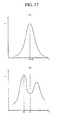
- FIG. 17 The horizontal axis of a graph of FIG. 17 represents the frequency of a resonant circuit of a noncontact IC card.
- the vertical axis indicates the absolute value of a receiving voltage occurring in the resonant circuit. This is similarly applied to the horizontal axis and the vertical axis of a later-described graph of FIG. 18.
- FIG. 17(A) shows a relationship between frequency and receiving voltage that occur when one noncontact IC card is brought close to an information read/write device.
- the noncontact IC card is used alone.
- resonant frequency f0 of the resonant circuit matches carrier frequency fc of a carrier signal transmitted from the information read/write device, and a high receiving voltage occurs at that frequency.
- FIG. 17(B) shows a relationship between frequency and receiving voltage that occur when two noncontact IC cards are overlaid with each other and brought close to the information read/write device.
- the two noncontact IC cards are overlaid and are subject to the influence of mutual inductance between the two noncontact IC cards, so that the resonant frequency of the resonant circuit varies and, as depicted in the Figure, the resonant frequency f0' deviates from the carrier frequency fc of the carrier signal from the information read/write device. For this reason, a low receiving voltage occurs at the carrier frequency fc as compared to the receiving voltage at the resonant frequency f0'. As a result, there arises a problem that sufficient electric power is not supplied to internal circuits of the noncontact IC card in use, leading to an inability to perform communication between reader/writer and the noncontact IC card.
- the resonant frequency of the noncontact IC card it has been proposed to preset the resonant frequency of the noncontact IC card such that it deviates to a higher frequency as compared to the carrier frequency. According to this method, the resonant frequency does not deviate so much from the carrier frequency even if the resonant frequency decreases when two noncontact IC cards are overlaid with each other and, therefore, it is possible to supply sufficient electric power to the internal circuits of the noncontact IC card in use.
- the noncontact IC card is set such that the resonant frequency f0 of its resonant circuit is higher than the carrier frequency fc as shown in FIG. 18(A) when the single noncontact IC card is used.
- FIG. 18(B) Shown in FIG. 18(B), on the other hand, is a case where two noncontact IC cards overlaid with each other are used. Since the two noncontact IC cards are used together and the two noncontact IC cards are subject to the influence of mutual inductance, the resonant frequency f0' becomes lower than the carrier frequency fc.
- the resonant frequency f0, f0' does not deviate so much from the carrier frequency fc as compared to the aforementioned case described with reference to FIG. 17. It is therefore possible to decrease the drop of induced electromotive force compared to the case described with reference to FIG. 17.
- Another previously proposed method is such that a switch is series-connected to the resonant circuit and a judgment is made to determine whether the noncontact IC card is overlaid with another noncontact IC card by monitoring the voltage of the resonant circuit while turning on and off the switch at random. If it is judged that the noncontact IC cards are overlaid with each other, the switch of one of the noncontact IC cards is turned off and the resonant circuit of the other noncontact IC card brought to a state of resonance. In this method, one noncontact IC card is in the state of resonance while the other noncontact IC card is not in the state of resonance when they are overlaid.
- the other noncontact IC card can receive energy of the resonant circuit of the first noncontact IC card thanks to electromagnetic coupling caused by mutual inductance.
- the intended voltage Japanese Laid-open Patent Publication No. 10-126318.
- a noncontact communications medium of this invention has the following structure.
- the resonant circuit when the antenna coil receives electromagnetic waves of a specific frequency, the resonant circuit resonates and a voltage Q times as high as the induced electromotive force occurs, where Q is the quality factor.
- the resonant circuit is a parallel-resonant circuit provided with the antenna coil and two capacitors. The two capacitors are connected parallel to each other.
- the capacitance change control means has a structure for varying the capacitance of the capacitor and is realized by a switch section and a switch control section described below.
- the switch section is formed of an analog switch for changing the resonant frequency of the resonant circuit.
- the analog switch is inserted into the resonant circuit in series with first one of the capacitors.
- the switch section When the switch section is turned on, the two parallel-connected capacitors and the antenna coil together constitute a resonant circuit in a connected state in which they are electrically connected.
- the switch section when the switch section is turned off, there is formed a resonant circuit in another connected state in which the first capacitor and the antenna coil are electrically disconnected and only the second capacitor is electrically connected to the antenna coil.
- the capacitance of the capacitor of the resonant circuit varies due to on/off operation of the switch section.
- the switch control section which has not been provided in conventional noncontact communications media, controls switching operation of the aforesaid switch section according to the amount of an output voltage occurring in the aforesaid resonant circuit and according to a specific change in the aforesaid output voltage.
- the aforementioned specific change means a relatively sharp rising edge of the output voltage of the resonant circuit, or a relatively sharp falling edge of the output voltage, that accompanies a change in the electromagnetic waves received by the resonant circuit.
- the output voltage from the resonant circuit increases to or beyond a specific value if an external communications apparatus with which communication should be carried out and the resonant circuit of the noncontact communications medium are electromagnetically coupled. If a relatively sharp rising edge or a relatively sharp falling edge constituting a specific change in the output voltage occurs when the amount of the output voltage is equal to or larger than the specific value, the switch control section compares the output voltage obtained when the first capacitor is set to the connected state by controlling the switch section with the output voltage obtained when the first capacitor is set to a disconnected state, and judges in which state the output voltage becomes higher.
- the output voltage of the resonant circuit becomes higher when the first capacitor is set to the connected state.
- the switch control section holds the switch section in the state in which the output voltage has become higher.
- the first capacitor is held in the connected state.
- the noncontact communications medium can maintain a state of resonance of the resonant circuit and supply sufficient electric power to the main circuit, so that the noncontact communications medium can carry out stable noncontact communication with the communications apparatus.
- the switch control section compares the output voltage obtained when the first capacitor is set to the connected state by controlling the switch section with the output voltage obtained when the first capacitor is set to the disconnected state, and judges in which state the output voltage becomes higher.
- the capacitance of the second capacitor is determined such that the resonant frequency of the resonant circuit and the frequency of the electromagnetic waves received by the antenna coil approximately match each other in each noncontact communications medium when the two noncontact communications media whose first capacitors are set to the disconnected state are overlaid with each other, the output voltage of the resonant circuit becomes higher when the first capacitor is set to the disconnected state in each noncontact communications medium.
- the switch control section holds the switch section in the state in which the output voltage has become higher.
- the first capacitor is held in the disconnected state.
- the two noncontact communications media can maintain a state of resonance of the resonant circuits and supply sufficient electric power to the main circuits, so that the two noncontact communications media can carry out stable noncontact communication with the communications apparatus.
- the resonant frequency of the resonant circuit becomes lower when three noncontact communications media are overlaid than when two noncontact communications media are overlaid.
- the capacitance of the second capacitor may be determined such that the resonant frequency of the resonant circuit becomes slightly higher than the frequency of the electromagnetic waves received by the antenna coil when two noncontact communications media whose first capacitors are set to the disconnected state are overlaid with each other. If this arrangement is used, the resonant frequency of the resonant circuit does not greatly deviate from the frequency of the electromagnetic waves in each noncontact communications medium when the aforesaid first capacitor is in the disconnected state, regardless of whether two noncontact communications media are overlaid or three noncontact communications media are overlaid.
- the capacitances of the two capacitors are to be determined such that the resonant frequency of the resonant circuit and the frequency of the electromagnetic waves received by the antenna coil approximately match each other in this case when the single noncontact communications medium is used with the aforesaid first capacitor in the connected state.
- the communication range of the noncontact communications medium does not decrease when used alone.
- the capacitances of the second capacitors should be made slightly small. This would be achieved if the capacitances of the first capacitor is made slightly larger and the frequency of the aforesaid electromagnetic waves and the resonant frequency of the aforesaid resonant circuit are made approximately equal to each other.
- the noncontact communications media become easier to overlay with each other and accommodate in a wallet or a pass holder by shaping them into a card form.
- the electric power for operating the main circuit is supplied after the amount of the output voltage of the resonant circuit has reached a sufficient voltage for operating the main circuit, it is possible to prevent malfunction of the main circuit potentially caused by insufficient electric power.
- the switch control section since the electric power is not supplied to the main circuit under the control of the switch control section until the amount of the output voltage of the resonant circuit occurring in the resonant circuit reaches a sufficient voltage for operating the main circuit, power consumption in the noncontact communications medium is low during that waiting period. Therefore, even if the noncontact communications medium is present within the communication range, in which the main circuit can communicate, and the output voltage of the noncontact communications medium is low, the switch control section operates, making it possible to determine the output of the switch control section. Then, the noncontact communications medium whose switch control section has been determined detects that an output voltage sufficient for operating the main circuit has occurred in the resonant circuit when the noncontact communications medium has been brought to the communication range at which the main circuit can operate. Since the noncontact communications medium begins to supply electric power for operating the main circuit by detecting this output voltage, the noncontact communications medium immediately begins to operate when it enters the communication range.
- the switch control section be held in the disconnected state in an initial state. This is because the analog switch is in its OFF state when the voltage of the electric power is equal to or lower than a specific voltage.
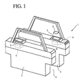
- FIG. 1 shows a noncontact IC card which is a noncontact communications medium according to an embodiment of the invention and a noncontact automatic ticket checker which performs radio communication with the noncontact IC card.
- This automatic ticket checker 1 comprises a pair of ticket checker units 3 facing each other on both sides of a ticket checker passage 2. There are provided doors (not shown) on side surfaces of the individual ticket checker units 3 for allowing or prohibiting passage of a user through the ticket checker passage 2.
- the ticket checker units 3 are each provided with an information read/write device 4.
- An antenna section 5 constituting part of the information read/write device 4 is provided on a top surface of each ticket checker unit 3 so that a wide area of communicability is obtained.
- a noncontact IC card 6 used as a ticket is placed within the communicability area of the information read/write device 4, noncontact data communication is performed between the noncontact IC card 6 and the information read/write device 4. More specifically, when a passenger, who is the user carrying the noncontact IC card 6, places it within the communicability area formed by the antenna section 5 of the information read/write device 4, the noncontact IC card 6 performs noncontact data communication concerning boarding information with the information read/write device 4.
- the automatic ticket checker 1 controls door opening/closing actions in accordance with the results of this communication, thereby allowing or prohibiting passage of the user such as the passenger.
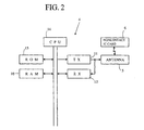
- FIG. 2 is a configuration diagram of the aforementioned information read/write device 4.
- the information read/write device 4 includes the antenna section 5, a transmitter section 11, a receiver section 12, a central processing unit (CPU) 14, a read-only memory (ROM) 15, and a random-access memory (RAM) 16.
- CPU central processing unit
- ROM read-only memory
- RAM random-access memory
- the transmitter section 11 generates a carrier for transmitting electric power to the noncontact IC card 6 and a high-frequency signal by modulating the aforementioned carrier for transmitting data, and supplies them to the antenna section 5.
- the receiver section 12 demodulates a signal received by the antenna section 5.
- the antenna section 5 is provided with a resonant circuit formed of an antenna coil and capacitors.
- the antenna section 5 transmits the modulated carrier fed from the transmitter section 11 in the form of electromagnetic waves via the resonant circuit.
- the noncontact IC card 6 receives the electromagnetic waves from the antenna section 5 and a resonant circuit provided in the noncontact IC card 6 produces a voltage.
- the configuration of the noncontact IC card 6 will be later described.
- the noncontact IC card 6 utilizes the voltage generated at this time as a power source.
- the noncontact IC card 6 also receives a signal transmitted from the antenna section 5, that is, the high-frequency signal obtained by modulating the carrier.
- An induced electromotive force generated by the antenna section 5 varies in the receiver section 12 due to changes in a magnetic field extending from the noncontact IC card 6 toward the antenna section 5. This enables the receiver section 12 to receive the signal transmitted from the noncontact IC card 6.
- the ROM 15 stores a program necessary for processing operation performed by the CPU 14 as well as data, such as user identification information and identification number of the noncontact IC card 6.
- the RAM 16 stores data to be transmitted to the automatic ticket checker 1 as well as data based on the received signal.
- the CPU 14 controls individual structural parts of the information read/write device 4 based on the data stored in the ROM 15 and the RAM 16.
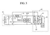
- FIG. 3 is a configuration diagram of the noncontact IC card.
- This noncontact IC card 6 includes an antenna coil L, two capacitors C1 C2, a switch element SW, a power circuit 62, a power supply switch element PSW, a switch control circuit 61, a demodulating circuit 64, a modulating circuit 65 and a data processing circuit 63.
- a resonant circuit 60 is formed of the antenna coil L and the two capacitors C1, C2.
- the capacitor C1 and the capacitor C2 are connected parallel to each other. Further, these capacitors C1, C2 are parallel-connected to the antenna coil L.
- the resonant circuit 60 is a parallel-resonant circuit formed of a coil and capacitors.
- the switch element SW is series-connected to the capacitor C2.
- the capacitor C2 is switched between a state in which the capacitor C2 is connected to the resonant circuit 60 and a state in which the capacitor C2 is disconnected from the resonant circuit 60, as the switch element SW is turned on or off.
- the resonant circuit 60 constitutes an antenna section, and the antenna coil L constitutes an antenna face of the antenna section.
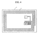
- the antenna coil L is a conductor pattern formed on a surface of the noncontact IC card 6 as illustrated in FIG. 4.
- the center of the noncontact IC card 6 approximately matches the center of the antenna coil L.
- the capacitances of the two capacitors C1, C2 are determined such that the resonant frequency of the resonant circuit 60 when the capacitor C2 is connected to the antenna coil L (when the switch element SW is on) approximately matches the frequency of the electromagnetic waves transmitted from the information read/write device 4. Also, the capacitance of the capacitor C1 is determined such that, when two noncontact IC cards 6 are overlaid with each other, with the capacitor C2 of each noncontact IC card 6 disconnected from the antenna coil L (i.e., the switch element SW is turned off), the resonant frequency of the resonant circuit 60 of each noncontact IC card 6 approximately matches the frequency of the electromagnetic waves transmitted from the ticket checker unit 3 under the influence of mutual inductance between these noncontact IC cards 6.
- the switch control circuit 61 produces a capacitor-connected state in which the capacitor C2 is connected to the resonant circuit 60 by controlling the switch element SW to turn on. Also, the switch control circuit 61 produces a capacitor-disconnected state in which the capacitor C2 is disconnected from the resonant circuit 60 by controlling the switch element SW to turn off.
- the resonant frequency of the resonant circuit 60 varies as a result of turning on and off of the switch element SW.
- the capacitor C2 corresponds to what is called a first capacitor in this invention, while the capacitor C1 corresponds to what is called a second capacitor in this invention.
- the power circuit 62 produces electric power used in the switch control circuit 61, the demodulating circuit 64, the modulating circuit 65 and the data processing circuit 63 by rectifying ac power generated in the resonant circuit 60 into dc power.
- the power circuit 62 also delivers a reset signal (Reset-A) which prohibits operation to the switch control circuit 61 when output voltage V of the power circuit 62 is less than a first threshold Vth1.
- this reset signal (Reset-A) has been entered, the switch control circuit 61 does not operate when the output voltage V of the power circuit 62 is less than the first threshold Vth1.
- the power supply switch element PSW is provided between the power circuit 62 and the demodulating circuit 64, the modulating circuit 65 and the data processing circuit 63.
- the switch control circuit 61 supplies electric power to the demodulating circuit 64, the modulating circuit 65 and the data processing circuit 63 by controlling the power supply switch element PSW to turn on. Also, the switch control circuit 61 interrupts power supply to the demodulating circuit 64, the modulating circuit 65 and the data processing circuit 63 by controlling the power supply switch element PSW to turn off.
- the demodulating circuit 64 demodulates a modulated carrier fed from the resonant circuit 60 and outputs a demodulated signal to the data processing circuit 63.
- the modulating circuit 65 modulates a signal fed from the data processing circuit 63 and outputs a resultant signal to the resonant circuit 60.
- the data processing circuit 63 stores specific data and performs such operations as to output a specific signal to the modulating circuit 65, store data corresponding to input/output signals, or modify the stored data in accordance with the signal entered from the demodulating circuit 64.
- the demodulating circuit 64, the modulating circuit 65 and the data processing circuit 63 are referred to as a data processing section 66 as a whole.
- This data processing section 66 corresponds to what is called a main circuit in this invention.
- the aforementioned switch control circuit 61 monitors the output voltage V rectified by the power circuit 62 and controls switching on/off of the switch element SW and the power supply switch element PSW based on the value of the output voltage V.
- FIG. 5 is a block diagram showing the functional configuration of the switch control circuit 61, in which the aforementioned reset signal (Reset-A) entered from the power circuit 62 to the switch control circuit 61 is not shown.
- the switch control circuit 61 includes a first voltage comparator 71, a second voltage comparator 72, a voltage change detector 73, a switch element switcher 74 and a state detector 75.
- the first voltage comparator 71 detects whether the output voltage V of the power circuit 62 has risen to or beyond the first threshold Vth1 and outputs a signal (Reset-B) indicating the result of detection.
- the second voltage comparator 72 detects whether the aforementioned output voltage V has risen to or beyond a second threshold Vth2 and outputs a signal (PSW control signal) indicating the result of detection.
- This PSW control signal is a signal which switches the power supply switch element PSW between ON and OFF states.
- the second threshold Vth2 is a voltage higher than the first threshold Vth1, and is a sufficient voltage for operating the data processing section 66.
- the voltage change detector 73 detects changes in the aforementioned output voltage V.
- the switch element switcher 74 outputs a signal which turns on and off the switch element SW.
- the state detector 75 compares the aforementioned output voltage V during OFF state and the output voltage V during ON state, judges in which state the output voltage V becomes higher, and outputs the result of detection. This judgment operation is referred to as detecting operation in this context.
- the noncontact IC card 6 performs this detecting operation when the aforementioned output voltage V is equal to or higher than the first threshold Vth1. Then, the noncontact IC card 6 maintains the state of the switch element SW (ON or OFF state of the switch element SW) in which the output voltage V becomes higher, and waits in that state until the output voltage V becomes equal to or higher than the second threshold Vth2.
- the noncontact IC card 6 of this embodiment is in its initial state when it is kept sufficiently far away from the antenna section 5 of the ticket checker unit 3 and the output voltage V of the power circuit 62 is less than the first threshold Vth1.
- FIGS. 7, 9 and 11 With respect to this initial state and later-described states 1 to 6.
- both the switch element SW and the power supply switch element PSW are in their OFF state.
- the switch control circuit 61 When the output voltage V of the power circuit 62 is less than the first threshold Vth1, the switch control circuit 61 does not operate because the reset signal (Reset-A) which prohibits the operation is entered from the power circuit 62. Thus, when the aforementioned output voltage V is less than the first threshold Vth1, the first voltage comparator 71 would in no case erroneously detect that the aforementioned output voltage V is equal to or higher than the first threshold Vth1 thereby causing the switch control circuit 61 to erroneously start the operation described below.
- the output voltage V of the aforementioned power circuit 62 rises as the noncontact IC card 6 approaches the antenna section 5 of the ticket checker unit 3.
- the power circuit 62 stops to enter the aforementioned reset signal (Reset-A) into the switch control circuit 61.
- the switch control circuit 61 of the noncontact IC card 6 starts to operate and the first voltage comparator 71 detects that the aforementioned output voltage V is equal to or higher than the first threshold Vth1.
- state 1 is the condition in which both the switch element SW and the power supply switch element PSW are in their OFF state.
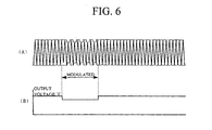
- the ticket checker unit 3 transmits a polling command to any noncontact IC card 6 which is placed within the communicability area at specific time intervals (e.g., every 10 ms) requesting the noncontact IC card 6 to return a response. Since the electromagnetic wave transmitted from the ticket checker unit 3 is modulated as shown in FIG. 6(A), the output voltage V of the power circuit 62 slightly drops as shown in FIG. 6(B) at this time.
- the detecting operation is performed to determine the state of the switch element SW in which the output voltage V becomes higher by turning on and off the switch element SW more than once while this polling command is being received (during the reception of the modulated wave)
- the noncontact IC card 6 of the present embodiment carries out the operation described below to correctly determine the state of the switch element SW in which the aforementioned output voltage V becomes higher.
- the output voltage V of the power circuit 62 is at a low level because the electromagnetic wave transmitted from the ticket checker unit 3 is modulated. It is possible to detect the end of transmission of the aforementioned polling command by detecting a rising edge of the output voltage V.
- the voltage change detector 73 serves to detect this rising edge of the output voltage V.
- the noncontact IC card 6 initiates the aforementioned detecting operation by reference to the detected rising edge of the output voltage V. This makes it possible to perform the detecting operation in a period other than when the electromagnetic wave transmitted from the ticket checker unit 3 is modulated and to synchronize execution of the detecting operation in each of the multiple noncontact IC cards 6 when they are overlaid. As a consequence, the noncontact IC card 6 can correctly determine the state of the switch element SW in which the aforementioned output voltage V becomes higher.
- the aforementioned detecting operation can be performed within a shorter period (e.g., 4 to 5 ms) than the polling command transmitting time interval (10 ms).
- the rising edge of the output voltage V of the power circuit 62 at the end of transmission of the aforementioned polling command from the ticket checker unit 3 is relatively sharp.
- rising of the output voltage V of the power circuit 62 when the noncontact IC card 6 is brought close to the antenna section 5 of the ticket checker unit 3 is relatively slow.
- the voltage change detector 73 detects the relatively sharp rising edge of the aforementioned output voltage V as the end of transmission of the aforementioned polling command from the ticket checker unit 3, but the voltage change detector 73 does not detect the relatively slow rising of the output voltage V as the end of transmission of the aforementioned polling command.
- the voltage change detector 73 detects the sharp rising edge of the output voltage V when the output voltage V of the aforementioned power circuit 62 is equal to or higher than the first threshold Vth1.
- the voltage change detector 73 detects this rising edge of the output voltage V.
- This condition is referred to as state 2 for the convenience of explanation.
- the state 2 is the condition in which the detecting operation is executed by turning on and off the switch element SW more than once at the fixed time intervals.
- the state 2 is also the condition in which the power supply switch element PSW is fixed to its OFF state.
- the noncontact IC card 6 causes the switch element SW to turn on and off more than once at the fixed time intervals in the detecting operation. This is intended to enable a plurality of noncontact IC cards 6 become on and off almost simultaneously. If a judgment is made that the output voltage V of the power circuit 62 becomes higher when the switch element SW is on than when the switch element SW is off, the switch element SW is maintained in its ON state. This condition is referred to as state 3 for the convenience of explanation.
- the state 3 is the condition in which the switch element SW is on and the power supply switch element PSW is off.
- the noncontact IC card 6 holds the switch element SW in its OFF state.
- This condition is referred to as state 4 for the convenience of explanation.
- the state 4 is the condition in which both the switch element SW and the power supply switch element PSW are in their OFF state.
- the capacitor C2 is electrically connected to the resonant circuit 60 when the switch element SW is on, and the capacitor C2 is electrically disconnected from the resonant circuit 60 when the switch element SW is off.
- the switch control circuit 61 further controls the power supply switch element PSW in the following fashion.
- the noncontact IC card 6 causes the power supply switch element PSW to turn on.
- a condition in which the power supply switch element PSW has become ON from the state 3 is referred to as state 5 for the convenience of explanation.
- a condition in which the power supply switch element PSW has become ON from the state 4 is referred to as state 6 for the convenience of explanation.
- the state 5 is the condition in which both the switch element SW and the power supply switch element PSW are in their ON state
- the state 6 is the condition in which switch element SW is in its OFF state and the power supply switch element PSW is in its ON state.
- the state 5 is a condition in which the two capacitors C1, C2 connected parallel to the antenna coil L are connected.
- the state 6 is a condition in which the capacitor C1 is connected but the capacitor C2 is not connected to the antenna coil L. While the resonant frequency of the resonant circuit 60 differs between the state 5 or the state 6, the output voltage V of the power circuit 62 rises beyond the specific threshold Vth2 and a voltage sufficient for operating the data processing section 66 is obtained in either of these states. Described below in detail are reasons why this situation is realized.
- FIG. 7 is a diagram showing results of control operation performed by the switch control circuit 61 over the switch element SW and the power supply switch element PSW when the noncontact IC card 6 is brought close to the antenna section 5 of the ticket checker unit 3.
- the switch element SW In the initial state, the switch element SW is in its OFF state, and the power supply switch element PSW is also in its OFF state.
- an induced electromotive force occurs in the resonant circuit 60 of the noncontact IC card 6 and the output voltage V of the power circuit 62 rises.
- the power circuit 62 stops to enter the reset signal (Reset-A) to the switch control circuit 61, causing the switch control circuit 61 to initiate its operation.
- the first voltage comparator 71 of the switch control circuit 61 detects that the output voltage V has become equal to or higher than the specified threshold Vth1, the noncontact IC card 6 goes into the state 1.
- the noncontact IC card 6 executes the detecting operation to determine the state of the switch element SW in which the output voltage V of the power circuit 62 becomes higher by turning on and off the switch element SW more than once.
- the capacitances of the two capacitors C1, C2 are determined such that the resonant frequency of the resonant circuit 60 when the capacitor C2 is connected to the antenna coil L approximately matches the frequency of the electromagnetic waves transmitted from the ticket checker unit 3.
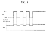
- FIG. 8(A) shows ON/OFF states of the switch element SW
- FIG. 8(B) shows the output voltage V of the power circuit 62.
- the noncontact IC card 6 goes into the state 3 in which the switch control circuit 61 holds the switch element SW in the ON state.
- the resonant frequency of the resonant circuit 60 approximately matches the frequency of the electromagnetic waves transmitted from the ticket checker unit 3.
- the second voltage comparator 72 detects that the output voltage V of the power circuit 62 has risen to or beyond the second threshold Vth2, and the noncontact IC card 6 goes into the state 5 in which the power supply switch element PSW is in the ON state.
- the noncontact IC card 6 When the noncontact IC card 6 is brought close to the antenna section 5 of the ticket checker unit 3, the noncontact IC card 6 shifts from its initial state to the state 1, state 2, state 3 and state 5 in this order as seen above and becomes ready to perform noncontact data communication.
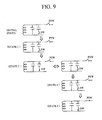
- FIG. 9 is a diagram showing results of control operation performed by the switch control circuit 61 over the switch element SW and the power supply switch element PSW when two noncontact IC cards 6 overlaid with each other are brought close to the antenna section 5 of the ticket checker unit 3.
- the two noncontact IC cards 6 perform generally the same operation. The following explanation deals with the operation of one of these noncontact IC cards 6.
- the switch element SW and the power supply switch element PSW are in their OFF state.
- an induced electromotive force occurs in the resonant circuit 60 of each noncontact IC card 6 and the output voltage V of the power circuit 62 rises.
- the power circuit 62 stops to enter the reset signal (Reset-A) to the switch control circuit 61, causing the switch control circuit 61 to initiate its operation.
- the first voltage comparator 71 of the switch control circuit 61 detects that the output voltage V has become equal to or higher than the specified threshold Vth1, the noncontact IC card 6 goes into the state 1.
- the two noncontact IC cards 6 go into the state 2 as each of the voltage change detectors 73 detects a rising edge of the output voltage V of the power circuit 62 at the same time. Then, each of the noncontact IC cards 6 executes the detecting operation to determine the state of the switch element SW in which the output voltage V of the power circuit 62 becomes higher by turning on and off the switch element SW. Thus, the detecting operation performed by the two noncontact IC cards 6 is synchronized.
- the output voltage V rises to or beyond the first threshold Vth1 due to the induced electromotive force occurring in the respective resonant circuits 60 almost simultaneously, or the output voltage V in one noncontact IC card 6 first rises to or beyond the first threshold Vth1 and the output voltage V in the other noncontact IC card 6 rises to or beyond the first threshold Vth1.
- the output voltage V of the power circuit 62 rises to or beyond the first threshold Vth1 in both of the two noncontact IC cards 6, and the voltage change detector 73 detects the rising edge of the output voltage V of the power circuit 62.
- the voltage change detectors 73 of the two noncontact IC cards 6 simultaneously detect the rising edge of the output voltage V of the respective power circuits 62. Consequently, the two noncontact IC cards 6 simultaneously go into the state 2 and initiate the detecting operation.
- the two noncontact IC cards 6 initiate the detecting operation by reference to the end of transmission of the polling command from the ticket checker unit 3 in this fashion.
- the two noncontact IC cards 6 are preset to become on and off at fixed time intervals, they turn on and off the respective switch elements SW at the same timing.
- the capacitance of the capacitor C1 is determined such that, when the two noncontact IC cards 6 in which the capacitor C2 is connected to the antenna coil L are overlaid with each other, the resonant frequency of the resonant circuit 60 of each noncontact IC card 6 approximately matches the frequency of the electromagnetic waves transmitted from the ticket checker unit 3 under the influence of mutual inductance between these noncontact IC cards 6.
- FIG. 10(A) shows ON/OFF states of the switch element SW
- FIG. 10(B) shows the output voltage V of the power circuit 62.
- the second voltage comparator 72 detects that the output voltage V of the power circuit 62 has risen to or beyond the second threshold Vth2, and the two noncontact IC cards 6 go into the state 6 in which the power supply switch element PSW is in the ON state.
- the two noncontact IC cards 6 can supply sufficient electric power to their data processing sections 66 even when the two noncontact IC cards 6 overlaid with each other are brought close to the antenna section 5 of the ticket checker unit 3. Therefore, both of the noncontact IC cards 6 become ready to perform noncontact data communication.
- each noncontact IC card 6 follows one of the aforementioned state transition flows. More specifically, when three or more overlaid noncontact IC cards 6 are used, each noncontact IC card 6 performs the detecting operation to determine the state (ON or OFF) of the switch element SW in which the output voltage of the power circuit 62 becomes higher, and holds the switch element SW in that state.
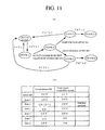
- FIG. 11(A) shows the state transition flow of the noncontact IC card 6
- FIG. 11(B) shows ON/OFF states of the switch element SW and the power supply switch element PSW in each state.
- both the switch element SW and the power supply switch element PSW are in their OFF state.
- the output voltage V of the power circuit 62 rises.
- the noncontact IC card 6 goes into the state 1.
- Both the switch element SW and the power supply switch element PSW are in their OFF state in this state 1 as well.
- the noncontact IC card 6 When the noncontact IC card 6 detects the end of transmission of the polling command from the ticket checker unit 3 in this state 1, the noncontact IC card 6 goes into the state 2 and initiates the detecting operation. In this detecting operation, the noncontact IC card 6 determines the state of the switch element SW in which the output voltage V of the power circuit 62 becomes higher by turning on and off the switch element SW more than once. More specifically, the noncontact IC card 6 determines the state of the switch element SW in which the difference between the resonant frequency of the resonant circuit 60 and the frequency of the electromagnetic waves transmitted from the ticket checker unit 3 becomes small.
- the noncontact IC card 6 goes into the state 3 in which the switch element SW is held in the ON state. Subsequently, the noncontact IC card 6 waits until the output voltage V rises to or beyond the second threshold Vth2 and goes into the state 5. In this state 5, the switch control circuit 61 holds the switch element SW and the power supply switch element PSW in their ON state. At this point, the noncontact IC card 6 supplies sufficient electric power to its data processing section 66 and can perform noncontact communication with the ticket checker unit 3.
- the noncontact IC card 6 Upon completion of noncontact communication with the ticket checker unit 3 in the state 5, the noncontact IC card 6 returns to the initial state. The noncontact IC card 6 also returns to the initial state when it is separated from the antenna section 5 and the output voltage V of the power circuit 62 drops to less than the first threshold Vth1.
- the noncontact IC card 6 goes into the state 4 in which the switch element SW is held in the OFF state. Subsequently, the noncontact IC card 6 waits until the output voltage V rises to or beyond the second threshold Vth2 and goes into the state 6. In this state 6, the switch control circuit 61 holds the switch element SW in the OFF state and the power supply switch element PSW in the ON state. At this point, the noncontact IC card 6 supplies sufficient electric power to its data processing section 66 and can perform noncontact communication with the ticket checker unit 3.
- the noncontact IC card 6 Upon completion of noncontact communication with the ticket checker unit 3 in the state 6, the noncontact IC card 6 returns to the initial state. The noncontact IC card 6 also returns to the initial state when it is separated from the antenna section 5 and the output voltage V of the power circuit 62 drops to less than the first threshold Vth1.
- the noncontact IC card 6 also returns to the initial state if the output voltage V of the power circuit 62 drops to less than the first threshold Vth1 when the noncontact IC card 6 is in the state 3 or state 4.
- the switch element SW is turned off.
- the aforementioned power supply switch element PSW need not necessarily be provided in the foregoing configuration, the electric power is always supplied from the power circuit 62 to the data processing section 66 if the power supply switch element PSW is not provided.
- the power supply switch element PSW it is possible to interrupt the power supply to the data processing section 66 by turning off the power supply switch element PSW and thereby reduce power consumption of the noncontact IC card 6.
- the data processing section 66 consumes greater electric power than the switch control circuit 61. Therefore, by interrupting the power supply to the data processing section 66, it is possible to operate the switch control circuit 61 with weaker electromagnetic waves than when the power supply to the data processing section 66 is not interrupted.
- FIG. 12 is a diagram showing time-sequential transition of the output voltage V of the power circuit 62 that occurs in one noncontact IC card 6 when the noncontact IC card 6 is brought close to the antenna section 5 of the information read/write device 4.
- the noncontact IC card 6 detects the end of transmission of a polling command (at time t5 shown in the Figure) when the output voltage V of the power circuit 62 is equal to or higher than the first threshold Vth1 (at time t3 or later shown in the Figure) when the output voltage V of the power circuit 62 is equal to or higher than the first threshold Vth1 (at time t3 or later shown in the Figure), the noncontact IC card 6 initiates the detecting operation.
- the period between times t1 and t2 and the period between times t4 and t5 are polling command transmitting periods.
- the switch element SW is held in the ON state at time t6. Since the resonant frequency of the resonant circuit 60 approximately matches the frequency of the electromagnetic wave transmitted from the ticket checker unit 3 as a consequence, the output voltage V of the power circuit 62 sharply rises. The output voltage V then continues to rise further. When the aforementioned output voltage reaches the second threshold Vth2 (time t7), the noncontact IC card 6 turns on the power supply switch element PSW. As a result, the noncontact IC card 6 begins to supply electric power to its main circuit and power consumption of the noncontact IC card 6 increases, so that the output voltage V rapidly drops down to voltage V3 (time t8).
- the output voltage V rises up to a saturation voltage V4 (time t9) and, subsequently, the output voltage becomes constant.
- a reason why the output voltage V sharply rises at time t6 is that the output voltage V instantly rises up to a voltage which should have been reached along a voltage-rising curve Q if the resonant circuit had been in a state of resonance from the beginning. Further, the output voltage rapidly drops down to the voltage V3 immediately after the power supply switch element PSW has becomes on.
- the second threshold Vth2 is set such that this output voltage V3 would become equal to or higher than a voltage necessary for operating the data processing section 66 which is the main circuit of the noncontact IC card 6.
- FIG. 13 is a diagram showing time-sequential transition of the output voltage V of the power circuit 62 that occurs in each noncontact IC card 6 when two noncontact IC cards 6 are brought close to the antenna section 5 of the information read/write device 4.
- the noncontact IC card 6 initiates the detecting operation. Based on results of this detecting operation, the switch element SW is held in the OFF state at time t6.
- the resonant frequency of the resonant circuit 60 which is affected by mutual inductance approximately matches the frequency of the electromagnetic wave transmitted from the ticket checker unit 3 in each noncontact IC card 6. Then, when the aforementioned output voltage reaches the second threshold Vth2 (time t7), the noncontact IC card 6 turns on the power supply switch element PSW. As a result, the noncontact IC card 6 begins to supply electric power to its main circuit and power consumption of the noncontact IC card 6 increases, so that the output voltage V rapidly drops down to voltage V3 (time t8). Then, the output voltage V rises up to a saturation voltage V4 (time t9) and, subsequently, the output voltage becomes constant.
- a reason why the output voltage V of the power circuit 62 does not sharply rise at time t6 is that the output voltage V has risen along a voltage-rising curve Q since the switch element SW is in the OFF state in the initial state of the noncontact IC card 6.
- FIG. 14 is a flowchart showing the operation of the switch control circuit 61.
- the switch element SW If the output voltage V of the power circuit 62 is higher when the switch element SW is on, the switch element SW is held in the OFF state (s5), and the noncontact IC card 6 waits until the output voltage V becomes equal to or higher than the first threshold Vth1 (s6) or equal to or higher than the second threshold Vth2 (s7). When the output voltage V becomes lower than the first threshold Vth1, the switch element SW is returned to OFF at s8 (s8) and the current operation is finished. As a result, the noncontact IC card 6 returns to the initial state.
- the power supply switch element PSW is turned on (s9).
- the switch element SW is held in the OFF state (s10), and the noncontact IC card 6 waits until the output voltage V becomes lower than the first threshold Vth1 (s11) or equal to or higher than the second threshold Vth2 (s12).
- the output voltage V becomes lower than the first threshold Vth1 the current operation is finished.
- the noncontact IC card 6 returns to the initial state.
- the power supply switch element PSW is turned on (s9).
- the noncontact IC card 6 returns to the initial state when noncontact communication with the ticket checker unit 3 is completed after the power supply switch element PSW has been turned on at s9.
- the noncontact IC card 6 also returns to the initial state when it is separated from the antenna section 5 and the output voltage V of the power circuit 62 drops to less than the first threshold Vth1.
- the capacitance of the capacitor C1 is determined such that, when two noncontact IC cards 6 are overlaid with each other, with the capacitor C2 of each noncontact IC card 6 disconnected from the antenna coil L, the resonant frequency of the resonant circuit 60 of each noncontact IC card 6 approximately matches the frequency of the electromagnetic waves transmitted from the ticket checker unit 3 under the influence of mutual inductance between these noncontact IC cards 6. This may be modified as described below.
- the capacitance of the capacitor C1 may be such that, when two noncontact IC cards 6 are overlaid with each other, with the capacitor C2 of each noncontact IC card 6 disconnected from the antenna coil L, the resonant frequency of the resonant circuit 60 of each noncontact IC card 6 is slightly higher than the frequency of the electromagnetic waves transmitted from the ticket checker unit 3 under the influence of mutual inductance between these noncontact IC cards 6.
- the capacitances of the two capacitors C1, C2 are determined such that, when the single noncontact IC card 6 is used, the resonant frequency of the resonant circuit 60 when the capacitor C2 is connected to the antenna coil L approximately matches the frequency of the electromagnetic waves transmitted from the ticket checker unit 3.
- the resonant frequency of the resonant circuit 60 becomes lower when three noncontact IC cards 6 are overlaid than when two noncontact IC cards 6 are overlaid. If the capacitances of the capacitors C1, C2 are determined as stated above and two noncontact IC cards 6 are overlaid, or three noncontact IC cards 6 are overlaid, the resonant frequency of the resonant circuit 60 of each noncontact IC card 6 does not greatly deviate from the frequency of the electromagnetic waves transmitted from the ticket checker unit 3 when the earlier-mentioned first capacitor C2 is in the disconnected state.
- the capacitances of the two capacitors C1, C2 are determined such that, when the single noncontact IC card 6 is used, the resonant frequency of the resonant circuit 60 when the capacitor C2 is connected to the antenna coil L approximately matches the frequency of the electromagnetic waves transmitted from the ticket checker unit 3, the communication range does not decrease when the single noncontact IC card 6 is used.
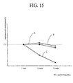
- Results of comparison between the noncontact IC card 6 of the present embodiment and a conventional noncontact IC card are shown in FIG. 15.
- Indicated by “A” is the result obtained when the resonant frequency is approximately matched to the frequency of the electromagnetic waves transmitted from the ticket checker unit 3 when two noncontact IC cards 6 whose switch elements SW are in the OFF state are overlaid with each other, and indicated by “B” is the result obtained when the resonant frequency is slightly increased.
- indicated by “C” is the result obtained with the conventional noncontact IC card. As shown in FIG.
- the noncontact IC cards 6 of this embodiment make it possible to avoid a drop of the resonant frequency by controlling ON/OFF actions of the switch element SW. Therefore, it is possible to perform noncontact communication with the ticket checker unit 3 even in a state where a plurality of noncontact IC cards 6 are overlaid with one another.
- the information read/write device 4 transmits a polling command at specific time intervals until a response to the polling command is received.
- the noncontact IC card 6 When any noncontact IC card 6 existing within the communicability area receives this polling command, the noncontact IC card 6 transmits a response containing its own identification information back to the information read/write device 4.
- noncontact IC cards 6 If a plurality of noncontact IC cards 6 exist within the same communicability area, such as when two or more noncontact IC cards 6 are overlaid, these noncontact IC cards 6 synchronize in operation. Therefore, responses to the polling command returned to the information read/write device 4 interfere with one another. In this circumstance, an anticollision treatment as described below, for example, is performed.
- the information read/write device 4 reexecutes polling operation.
- the polling command transmitted in this reexecuted polling operation is a different command from the polling command transmitted in the first polling operation.
- the first polling command is referred to as the polling command A and the second polling command is referred to as the polling command B.
- the multiple noncontact IC cards 6 which have received the polling command B individually return their responses to the information read/write device 4 with random time delays. This makes it possible to avoid interference of the responses from the individual noncontact IC cards 6.
- the information read/write device 4 If interference occurs even when the responses are returned with random time delays, the information read/write device 4 retransmits the polling command B, causing the noncontact IC cards 6 to randomly respond again. The information read/write device 4 repeatedly transmits the polling command B until the responses from the noncontact IC cards 6 do not interfere with one another. With this arrangement, the information read/write device 4 can receive interference-free responses from the individual noncontact IC cards 6.
- the information read/write device 4 receives the response from one noncontact IC card 6 (hereinafter referred to as the first noncontact IC card 6) at first. The information read/write device 4 then disregards the response transmitted subsequently from the other noncontact IC card 6 (hereinafter referred to as the second noncontact IC card 6). The information read/write device 4 determines from which noncontact IC card 6 the response has been received based on the identification information of the received response. To begin noncontact communication with the first noncontact IC card 6 from which the response has been received, the information read/write device 4 transmits a command for establishing communication to the first noncontact IC card 6. This communication-establishing command contains identification information of the first noncontact IC card 6.
- the first noncontact IC card 6 Upon receiving this communication-establishing command, the first noncontact IC card 6 transmits a response to the communication-establishing command back to the information read/write device 4.
- the information read/write device 4 transmits a read command, etc. to the first noncontact IC card 6.
- the first noncontact IC card 6 then transmits a response corresponding to the received command back to the information read/write device 4.
- Noncontact communication between the information read/write device 4 and the first noncontact IC card 6 is carried out in this manner.
- the information read/write device 4 retransmits the polling command. Since the noncontact communication is finished at this point, the first noncontact IC card 6 does not transmit any response to this polling command. The second noncontact IC card 6, which has not finished the noncontact communication transmits the response to this polling command.
- the information read/write device 4 Upon receiving this response, the information read/write device 4 transmits a communication-establishing command to the second noncontact IC card 6.
- the second noncontact IC card 6 transmits a response to this communication-establishing command back to the information read/write device 4.
- the information read/write device 4 transmits a read command, etc. to the second noncontact IC card 6.
- the second noncontact IC card 6 transmits a response corresponding to the received command back to the information read/write device 4.
- Noncontact communication between the information read/write device 4 and the second noncontact IC card 6 is carried out in this way.
- the information read/write device 4 transmits the polling command at specific times and performs noncontact communication with the noncontact IC card 6 which has returned the response to the communication-establishing command in the aforementioned manner.
- the method is described using an example in which two noncontact IC cards 6 are present within the communicability area.
- the information read/write device 4 transmits the polling command at specific time intervals until the response to the polling command is received.
- any noncontact IC card 6 existing within the communicability area receives this polling command, the noncontact IC card 6 transmits a response containing its own identification information back to the information read/write device 4. If interference occurs here, the anticollision treatment is performed. Let us now consider a case where one of two noncontact IC cards 6 transmits a response at an earlier time.
- the information read/write device 4 receives the response from one noncontact IC card 6 (hereinafter referred to as the first noncontact IC card 6) at first. Subsequently, the information read/write device 4 receives the response from the other noncontact IC card 6 (hereinafter referred to as the second noncontact IC card 6).
- the information read/write device 4 which has received the responses from the two noncontact IC cards 6 retransmits the polling command to judge whether there exists any other noncontact IC card 6 within the communicability area with which communication can be made. If the information read/write device 4 judges that no response is received from other noncontact IC card 6, the information read/write device 4 performs an operation for carrying out noncontact communication with the two noncontact IC cards 6.
- the information read/write device 4 determines from which noncontact IC card 6 each response has been received based on the identification information of the received response.
- the information read/write device 4 transmits a command for establishing communication to each noncontact IC card 6.
- the first noncontact IC card 6 Upon receiving this communication-establishing command, the first noncontact IC card 6 transmits a response to the communication-establishing command back to the information read/write device 4.
- the second noncontact IC card 6 also transmits a response to the communication-establishing command back to the information read/write device 4.
- the information read/write device 4 Upon receiving the responses to the communication-establishing commands from the individual noncontact IC cards 6, the information read/write device 4 transmits a read command, etc. to the first noncontact IC card 6. The first noncontact IC card 6 then transmits a response corresponding to the received command back to the information read/write device 4. Noncontact communication between the information read/write device 4 and the first noncontact IC card 6 is carried out in this manner.
- the information read/write device 4 transmits a read command, etc. to the second noncontact IC card 6.
- the second noncontact IC card 6 transmits a response corresponding to the received command back to the information read/write device 4.
- Noncontact communication between the information read/write device 4 and the second noncontact IC card 6 is carried out in this way.
- the information read/write device 4 transmits the polling command.
- the information read/write device 4 repeatedly transmits the polling command at specific time intervals until the response to the polling command is received.
- noncontact IC card 6 of the foregoing embodiment initiates the aforementioned detecting operation by reference to the timing of detecting the end of transmission of the polling command from the information read/write device 4, this may be modified as described below.
- an information read/write device 4 reduces electromagnetic wave output power for a specific time period at specific time intervals (e.g., every 20 ms) as shown in FIG. 16(A).
- electromagnetic waves transmitted from the information read/write device 4 are not modulated except when it is communicating with a noncontact IC card 6.
- output voltage V of a power circuit 62 drops for a specific time period at specific time intervals (e.g., every 10 ms) as shown in FIG. 16(B).
- the fixed time period during which the information read/write device 4 decreases the electromagnetic wave output power is a period (e.g., 2 ms) which is sufficient for executing the aforementioned detecting operation.
- the noncontact IC card 6 of this embodiment may detect a rising edge of the output voltage V and perform the aforementioned detecting operation by reference to the detected rising edge of the output voltage V.
- the noncontact IC card 6 may detect a falling edge of the output voltage V and perform the aforementioned detecting operation by reference to the detected falling edge of the output voltage V. In either case, the noncontact IC card 6 produces the same effects as the noncontact IC card 6 of the foregoing embodiment.
- the detecting operation performed by the noncontact IC card 6 of this embodiment is the same as that performed by the noncontact IC card 6 of the foregoing embodiment, except that the timing of executing the detecting operation differs.
- the noncontact IC card 6 and the information read/write device 4 communicate with each other by transmitting a communication request command requesting communication from the information read/write device 4 existing within the communicability area to the information read/write device 4.
- a specific communicability method is described below. Here, the method is described using an example in which two noncontact IC cards 6 are present within the communicability area.
- the two noncontact IC cards 6 existing within the communicability area individually transmit communication request commands requesting communication to the information read/write device 4. These communication request commands contain identification information which identifies the respective noncontact IC cards 6. Let us now consider a case where one of the two noncontact IC cards 6 transmits the communication request command at an earlier time.
- the information read/write device 4 When the information read/write device 4 receives the communication request command from one noncontact IC card 6 (hereinafter referred to as the first noncontact IC card 6) existing within the communicability area, the information read/write device 4 determines from which noncontact IC card 6 the communication request command has been received. To begin noncontact communication with the first noncontact IC card 6 from which the communication request command has been received, the information read/write device 4 transmits a command for establishing communication to the first noncontact IC card 6. This communication-establishing command contains the identification information of the first noncontact IC card 6.
- the first noncontact IC card 6 Upon receiving this communication-establishing command, the first noncontact IC card 6 transmits a response to the communication-establishing command back to the information read/write device 4.
- the information read/write device 4 When the response to the communication-establishing command is received from the first noncontact IC card 6, the information read/write device 4 transmits a read command, etc. to the first noncontact IC card 6. The first noncontact IC card 6 then transmits a response corresponding to the received command back to the information read/write device 4. Noncontact communication between the information read/write device 4 and the first noncontact IC card 6 is carried out in this manner.
- the information read/write device 4 waits for a communication request command to be transmitted from the second noncontact IC card 6 while carrying out the operation to reduce the electromagnetic wave output power for a specific time period at the specific time intervals.
- the communication request command is received from the second noncontact IC card 6
- the information read/write device 4 transmits a command for establishing communication to the second noncontact IC card 6 to begin noncontact communication with the second noncontact IC card 6.
- This communication-establishing command contains the identification information of the second noncontact IC card 6.
- the second noncontact IC card 6 Upon receiving this communication-establishing command, the second noncontact IC card 6 transmits a response to the communication-establishing command to the information read/write device 4.
- the information read/write device 4 When the response to the communication-establishing command is received from the second noncontact IC card 6, the information read/write device 4 transmits a read command, etc. to the second noncontact IC card 6. The second noncontact IC card 6 then transmits a response corresponding to the received command back to the information read/write device 4. Noncontact communication between the information read/write device 4 and the second noncontact IC card 6 is carried out in this manner.
- Communication between the information read/write device 4 and the noncontact IC card 6 may be carried out by the following method as well.
- the method is described using an example in which two noncontact IC cards 6 are present within the communicability area.
- both noncontact IC cards 6 transmit communication request commands requesting communication to the noncontact IC card 6.
- These communication request commands contain identification information which identifies the respective noncontact IC cards 6.
- the information read/write device 4 When the information read/write device 4 receives the communication request command from one noncontact IC card 6 (hereinafter referred to as the first noncontact IC card 6), the information read/write device 4 waits until the communication request command from the other noncontact IC card 6 (hereinafter referred to as the second noncontact IC card 6) for a preset time period. Here, the information read/write device 4 receives the communication request command from the second noncontact IC card 6. The information read/write device 4 transmits communication-establishing commands to the individual noncontact IC cards 6. Upon receiving the communication-establishing command, the first noncontact IC card 6 transmits a response to the command back to the information read/write device 4. Upon receiving the communication-establishing command, the second noncontact IC card 6 also transmits a response to the command back to the information read/write device 4.
- the information read/write device 4 Upon receiving the responses to the communication-establishing commands from the individual noncontact IC cards 6, the information read/write device 4 transmits a read command, etc. to the first noncontact IC card 6. The first noncontact IC card 6 then transmits a response corresponding to the received command back to the information read/write device 4. Noncontact communication between the information read/write device 4 and the first noncontact IC card 6 is carried out in this manner.
- the information read/write device 4 transmits a read command, etc. to the second noncontact IC card 6.
- the second noncontact IC card 6 transmits a response corresponding to the received command back to the information read/write device 4.
- Noncontact communication between the information read/write device 4 and the second noncontact IC card 6 is carried out in this way.
- the information read/write device 4 waits for a communication request command to be transmitted from another noncontact IC card 6 while carrying out the operation to reduce the electromagnetic wave output power for a specific time period at the specific time intervals (e.g., every 20 ms).
- noncontact communications media e.g., noncontact IC cards
- a communications apparatus such as an information read/write device
- This invention applied to such equipment as identification equipment, a personal authentication apparatus, an automatic ticket checker, an automated teller machine for handling cash or electronic cash, and a charge collecting machine.
Landscapes
- Engineering & Computer Science (AREA)
- Microelectronics & Electronic Packaging (AREA)
- Computer Hardware Design (AREA)
- Physics & Mathematics (AREA)
- General Physics & Mathematics (AREA)
- Theoretical Computer Science (AREA)
- Computer Networks & Wireless Communication (AREA)
- Near-Field Transmission Systems (AREA)
- Devices For Checking Fares Or Tickets At Control Points (AREA)
- Dc-Dc Converters (AREA)
- Developing Agents For Electrophotography (AREA)
- Radar Systems Or Details Thereof (AREA)
Abstract
Description
Claims (15)
- A noncontact communications medium comprising:capacitance change control means which varies the capacitance of said capacitor according to the amount of an output voltage occurring in said resonant circuit and according to a specific change in said output voltage.a resonant circuit including:an antenna coil which generates an induced electromotive force and thereby transmits and receives signals by receiving electromagnetic waves carrying information as a result of changes in the amount of electric power; anda capacitor parallel-connected to the antenna coil; a main circuit which processes a received signal obtained by demodulating an output of said resonant circuit and outputs a modulated transmitting signal to said resonant circuit; and
- A noncontact communications medium comprising:a resonant circuit including:an antenna coil which generates an induced electromotive force and thereby transmits and receives signals by receiving electromagnetic waves carrying information as a result of changes in the amount of electric power; and two capacitors parallel-connected to the antenna coil;a main circuit which processes a received signal obtained by demodulating an output of said resonant circuit and outputs a modulated transmitting signal to said resonant circuit;a switch section which switches first one of said two capacitors between a connected state and a disconnected state; anda switch control section which controls switching operation of said switch section according to the amount of an output voltage occurring in said resonant circuit and according to a specific change in said output voltage.
- The noncontact communications medium as recited in claim 2, wherein said switch control section controls the switching operation of said switch section according to a specific change in said output voltage when the output voltage occurring in said resonant circuit is equal to or higher than a specific value.
- The noncontact communications medium as recited in claim 2, wherein said switch control section controls the switching operation of said switch section according to a change at a rising edge of said output voltage when the output voltage occurring in said resonant circuit is equal to or higher than a specific value.
- The noncontact communications medium as recited in claim 2, wherein said switch control section controls the switching operation of said switch section according to a change at a falling edge of said output voltage when the output voltage occurring in said resonant circuit is equal to or higher than a specific value.
- The noncontact communications medium as recited in claim 2, wherein said switch control section judges whether the output voltage occurring in said resonant circuit becomes higher when said first capacitor is in the connected state or in the disconnected state when the switching operation of said switch section is controlled, and holds said switch section in the state in which said output voltage becomes higher.
- The noncontact communications medium as recited in claim 6, wherein said switch control section causes said main circuit to operate after holding said switch section.
- The noncontact communications medium as recited in claim 6, wherein said switch control section begins to supply electric power for operating said main circuit after the amount of said output voltage has reached a sufficient voltage for operating said main circuit under conditions in which said switch section is held.
- The noncontact communications medium as recited in claim 2, wherein the capacitance of the second capacitor is such that, when the noncontact communications medium is overlaid with another one with said first capacitor set in the disconnected state in each noncontact communications medium, the frequency of said electromagnetic waves and the resonant frequency of the two noncontact communications media approximately match each other.
- The noncontact communications medium as recited in claim 9, wherein the capacitances of said two capacitors are such that, when said first capacitor is in the connected state, the frequency of said electromagnetic waves and the resonant frequency of said resonant circuit approximately match each other.
- The noncontact communications medium as recited in claim 2, wherein the capacitance of the second capacitor is such that, when the noncontact communications medium is overlaid with another one with said first capacitor set in the disconnected state in each noncontact communications medium, the resonant frequency of the two noncontact communications media becomes higher than the frequency of said electromagnetic waves.
- The noncontact communications medium as recited in claim 11, wherein the capacitances of said two capacitors are such that, when said first capacitor is in the connected state, the frequency of said electromagnetic waves and the resonant frequency of said resonant circuit approximately match each other.
- The noncontact communications medium as recited in claim 2, wherein said switch control section holds said first capacitor in the disconnected state in an initial state.
- The noncontact communications medium as recited in claim 2, wherein the noncontact communications medium is card-shaped in external appearance.
- A noncontact communications system comprising:a noncontact communications medium which comprises:a resonant circuit including:an antenna coil which generates an induced electromotive force and thereby transmits and receives signals by receiving electromagnetic waves carrying information as a result of changes in the amount of electric power; andtwo capacitors parallel-connected to the antenna coil;a main circuit which processes a received signal obtained by demodulating an output of said resonant circuit and outputs a modulated transmitting signal to said resonant circuit;a switch section which switches first one of said two capacitors between a connected state and a disconnected state; anda switch control section which controls switching operation of said switch section according to the amount of an output voltage occurring in said resonant circuit and according to a specific change in said output voltage; anda communications apparatus which communicates with said noncontact communications medium by radio.
Applications Claiming Priority (3)
| Application Number | Priority Date | Filing Date | Title |
|---|---|---|---|
| JP2000246349 | 2000-08-15 | ||
| JP2000246349 | 2000-08-15 | ||
| PCT/JP2001/004923 WO2002015124A1 (en) | 2000-08-15 | 2001-06-11 | Noncontact communication medium and noncontact communication system |
Publications (3)
| Publication Number | Publication Date |
|---|---|
| EP1327958A1 true EP1327958A1 (en) | 2003-07-16 |
| EP1327958A4 EP1327958A4 (en) | 2005-05-11 |
| EP1327958B1 EP1327958B1 (en) | 2008-04-23 |
Family
ID=18736679
Family Applications (1)
| Application Number | Title | Priority Date | Filing Date |
|---|---|---|---|
| EP01936953A Expired - Lifetime EP1327958B1 (en) | 2000-08-15 | 2001-06-11 | Non contact communication medium and system |
Country Status (9)
| Country | Link |
|---|---|
| US (1) | US6952167B2 (en) |
| EP (1) | EP1327958B1 (en) |
| JP (1) | JP3843944B2 (en) |
| CN (1) | CN1185599C (en) |
| AT (1) | ATE393435T1 (en) |
| AU (1) | AU2001262739A1 (en) |
| DE (1) | DE60133755T2 (en) |
| TW (1) | TW516284B (en) |
| WO (1) | WO2002015124A1 (en) |
Cited By (5)
| Publication number | Priority date | Publication date | Assignee | Title |
|---|---|---|---|---|
| EP1387313A3 (en) * | 2002-07-30 | 2004-06-23 | Omron Corporation | RFID-tag with tuning means and anticollision method |
| WO2005048181A1 (en) * | 2003-11-04 | 2005-05-26 | Avery Dennison Corporation | Rfid tag with enhanced readability |
| EP1870981A2 (en) | 2004-08-04 | 2007-12-26 | Seiko Epson Corporation | Power supply monitoring circuit unit using same, and display device for electronic paper |
| EP2133826A1 (en) * | 2008-06-13 | 2009-12-16 | Fujitsu Ltd. | RFID tag with improved reading range |
| EP2188867A4 (en) * | 2007-09-13 | 2014-12-10 | Qualcomm Inc | Antennas for wireless power applications |
Families Citing this family (40)
| Publication number | Priority date | Publication date | Assignee | Title |
|---|---|---|---|---|
| US6472975B1 (en) * | 1994-06-20 | 2002-10-29 | Avid Marketing, Inc. | Electronic identification system with improved sensitivity |
| US7501954B1 (en) * | 2000-10-11 | 2009-03-10 | Avante International Technology, Inc. | Dual circuit RF identification tags |
| DE10227558A1 (en) * | 2002-06-20 | 2004-01-15 | Infineon Technologies Ag | System for data exchange between at least two contactless data carriers |
| CN100378755C (en) * | 2002-07-30 | 2008-04-02 | Nxp股份有限公司 | Repeater with controllable power-on-reset circuit |
| US6863220B2 (en) * | 2002-12-31 | 2005-03-08 | Massachusetts Institute Of Technology | Manually operated switch for enabling and disabling an RFID card |
| CN1813384B (en) * | 2003-05-23 | 2011-05-11 | 奥克兰联合服务有限公司 | Methods and apparatus for control of inductively coupled power transfer systems |
| KR100739410B1 (en) * | 2003-07-17 | 2007-07-24 | 혼다 기켄 고교 가부시키가이샤 | Ic card and information storage/transmitter |
| DE10334398B4 (en) * | 2003-07-28 | 2008-04-03 | Siemens Ag | Method for reducing the power consumption of a mobile data memory, application of the method in an identification system with at least one read / write device and a mobile data memory |
| JP4244169B2 (en) * | 2003-08-04 | 2009-03-25 | 日本発條株式会社 | Non-contact information medium and communication system using the same |
| JP4036813B2 (en) * | 2003-09-30 | 2008-01-23 | シャープ株式会社 | Non-contact power supply system |
| JP4519476B2 (en) * | 2004-02-03 | 2010-08-04 | 株式会社東芝 | Wireless communication device |
| US7132946B2 (en) * | 2004-04-08 | 2006-11-07 | 3M Innovative Properties Company | Variable frequency radio frequency identification (RFID) tags |
| KR20040072581A (en) | 2004-07-29 | 2004-08-18 | (주)제이씨 프로텍 | An amplification relay device of electromagnetic wave and a radio electric power conversion apparatus using the above device |
| CN100418105C (en) * | 2004-08-24 | 2008-09-10 | 曾超宁 | Intelligently controlled radio frequency IC card |
| JP2008009464A (en) * | 2004-10-13 | 2008-01-17 | Tatsuya Hisagane | Card type computer |
| WO2007023472A2 (en) | 2005-08-25 | 2007-03-01 | Nxp B.V. | Method and rfid reader for evaluating a data stream signal in respect of data and/or collision |
| FR2890501A1 (en) * | 2005-09-02 | 2007-03-09 | St Microelectronics Sa | NON-CONTACT PASSIVE INTEGRATED CIRCUIT COMPRISING AN ANTENNA IMPEDANCE MODULATION SWITCH NOT INHIBITING A PRIMARY LOAD PUMP |
| US8038070B2 (en) * | 2005-10-18 | 2011-10-18 | Panasonic Corporation | Noncontact data carrier |
| JP2007334507A (en) | 2006-06-13 | 2007-12-27 | Felica Networks Inc | Integrated circuit, non-contact type ic card, reader/writer, radio communication method and computer program |
| US7570220B2 (en) * | 2006-06-27 | 2009-08-04 | Sensormatic Electronics Corporation | Resonant circuit tuning system with dynamic impedance matching |
| EP1873692B1 (en) * | 2006-06-29 | 2011-12-21 | Semiconductor Energy Laboratory Co., Ltd. | Semiconductor device |
| US8243049B2 (en) * | 2006-12-20 | 2012-08-14 | 3M Innovative Properties Company | Untethered stylus employing low current power converter |
| JP5222628B2 (en) | 2007-05-31 | 2013-06-26 | 株式会社半導体エネルギー研究所 | Semiconductor device |
| JP2009054061A (en) * | 2007-08-29 | 2009-03-12 | Renesas Technology Corp | Semiconductor device |
| JP2009081943A (en) * | 2007-09-26 | 2009-04-16 | Seiko Epson Corp | Power transmission control device, power transmission device, power transmission side device, and non-contact power transmission system |
| EP2053546A1 (en) * | 2007-10-26 | 2009-04-29 | Gemplus | Radiofrequency communication device comprising a timer |
| US7652578B2 (en) * | 2007-10-29 | 2010-01-26 | Motorola, Inc. | Detection apparatus and method for near field communication devices |
| WO2009066211A2 (en) | 2007-11-19 | 2009-05-28 | Nxp B.V. | Transceiving circuit for contactless communication |
| EP2557528A3 (en) * | 2007-12-26 | 2017-01-18 | Murata Manufacturing Co., Ltd. | Antenna device and wireless IC device |
| JP2009176027A (en) * | 2008-01-24 | 2009-08-06 | Toshiba Corp | Wireless communication apparatus and wireless communication system |
| JP5483030B2 (en) | 2008-03-17 | 2014-05-07 | パワーマット テクノロジーズ リミテッド | Inductive transmission system |
| US8981598B2 (en) | 2008-07-02 | 2015-03-17 | Powermat Technologies Ltd. | Energy efficient inductive power transmission system and method |
| US11979201B2 (en) | 2008-07-02 | 2024-05-07 | Powermat Technologies Ltd. | System and method for coded communication signals regulating inductive power transmissions |
| JP2010204986A (en) * | 2009-03-04 | 2010-09-16 | Sony Corp | Communication device, communication method, and program |
| WO2011024844A1 (en) * | 2009-08-26 | 2011-03-03 | 凸版印刷株式会社 | Non-contact communication medium |
| EP2407915A1 (en) | 2010-07-16 | 2012-01-18 | Nagravision S.A. | Multiple-speed interface |
| JP5041610B2 (en) * | 2010-11-01 | 2012-10-03 | 則雄 宮内 | Wireless charging apparatus and wireless charging method thereof |
| EP2798910B1 (en) * | 2011-12-29 | 2017-06-21 | Arçelik Anonim Sirketi | A wireless kitchen appliance operated on an induction heating cooker |
| KR101436063B1 (en) * | 2012-10-18 | 2014-08-29 | (주)기술과가치 | Wiress Power Transmission Apparatus |
| US20160087480A1 (en) * | 2014-09-23 | 2016-03-24 | Qualcomm Incorporated | Charging Apparatus Including Remote Device Reset |
Family Cites Families (22)
| Publication number | Priority date | Publication date | Assignee | Title |
|---|---|---|---|---|
| JP3068745B2 (en) * | 1994-05-27 | 2000-07-24 | ローム株式会社 | High-frequency tag and information exchange system using it |
| DE3922977A1 (en) | 1989-07-12 | 1991-01-24 | Texas Instruments Deutschland | TRIMMING AND USE OF SUCH TRIMMING EXECUTIBLE MATCHING METHOD |
| DE4327642C2 (en) | 1993-05-17 | 1998-09-24 | Anatoli Stobbe | Reader for a detection plate |
| JP3962099B2 (en) * | 1994-05-27 | 2007-08-22 | ローム株式会社 | High frequency tag and information exchange system using the same |
| JPH087059A (en) * | 1994-06-21 | 1996-01-12 | Sony Chem Corp | Contactless information card |
| DE4438287C1 (en) | 1994-10-26 | 1996-05-09 | Siemens Ag | System for contactless energy and data transmission |
| JPH09218263A (en) * | 1995-10-11 | 1997-08-19 | Texas Instr Inc <Ti> | Transponder system and operating method thereof |
| DE19614455A1 (en) * | 1996-04-12 | 1997-10-16 | Philips Patentverwaltung | Method for operating a system from a base station and a transponder coupled to it in a contactless manner, and a suitable system for this |
| DE19621076C2 (en) * | 1996-05-24 | 2001-06-28 | Siemens Ag | Device and method for the contactless transmission of energy or data |
| JP3392016B2 (en) * | 1996-09-13 | 2003-03-31 | 株式会社日立製作所 | Power transmission system and power transmission and information communication system |
| JPH10126318A (en) | 1996-10-11 | 1998-05-15 | Omron Corp | Contactless medium and contactless transmission system |
| FR2757952B1 (en) * | 1996-12-27 | 1999-03-19 | Gemplus Card Int | RADIO TRANSPONDER PROVIDED WITH AN ANTENNA AND A FREQUENCY TUNING CIRCUIT |
| JPH10187916A (en) * | 1996-12-27 | 1998-07-21 | Rohm Co Ltd | Transponder in contactless IC card communication system |
| GB2321726A (en) | 1997-01-30 | 1998-08-05 | Motorola Inc | Apparatus and method for regulating power on a contactless portable data carrier |
| JPH10269327A (en) | 1997-03-27 | 1998-10-09 | Hitachi Ltd | Control circuit |
| JPH10320519A (en) | 1997-05-19 | 1998-12-04 | Rohm Co Ltd | Transponder in IC card communication system |
| FR2782209A1 (en) * | 1998-08-06 | 2000-02-11 | Innovatron Electronique | Inductively-read transponder for access control or payment, switches in capacitor to detune resonant circuit if supply voltage derived from read signal is excessive |
| JP3478143B2 (en) | 1998-10-20 | 2003-12-15 | オムロン株式会社 | Contactless communication method, contactless communication medium, contactless communication device, boarding card and automatic ticket gate |
| JP2000151480A (en) * | 1998-11-11 | 2000-05-30 | Mitsubishi Materials Corp | Identification method for superimposed tags |
| FR2792134B1 (en) | 1999-04-07 | 2001-06-22 | St Microelectronics Sa | DISTANCE DETECTION BETWEEN AN ELECTROMAGNETIC TRANSPONDER AND A TERMINAL |
| JP3800091B2 (en) | 2000-02-10 | 2006-07-19 | オムロン株式会社 | Non-contact communication medium and non-contact communication system |
| JP3488166B2 (en) | 2000-02-24 | 2004-01-19 | 日本電信電話株式会社 | Contactless IC card system, its reader / writer and contactless IC card |
-
2001
- 2001-06-11 US US10/344,375 patent/US6952167B2/en not_active Expired - Fee Related
- 2001-06-11 EP EP01936953A patent/EP1327958B1/en not_active Expired - Lifetime
- 2001-06-11 CN CN01814259.1A patent/CN1185599C/en not_active Expired - Fee Related
- 2001-06-11 WO PCT/JP2001/004923 patent/WO2002015124A1/en not_active Ceased
- 2001-06-11 DE DE60133755T patent/DE60133755T2/en not_active Expired - Fee Related
- 2001-06-11 AT AT01936953T patent/ATE393435T1/en not_active IP Right Cessation
- 2001-06-11 AU AU2001262739A patent/AU2001262739A1/en not_active Abandoned
- 2001-06-11 JP JP2002520176A patent/JP3843944B2/en not_active Expired - Fee Related
- 2001-08-08 TW TW090119352A patent/TW516284B/en not_active IP Right Cessation
Cited By (11)
| Publication number | Priority date | Publication date | Assignee | Title |
|---|---|---|---|---|
| EP1387313A3 (en) * | 2002-07-30 | 2004-06-23 | Omron Corporation | RFID-tag with tuning means and anticollision method |
| WO2005048181A1 (en) * | 2003-11-04 | 2005-05-26 | Avery Dennison Corporation | Rfid tag with enhanced readability |
| US7298330B2 (en) | 2003-11-04 | 2007-11-20 | Avery Dennison Corporation | RFID tag with enhanced readability |
| US7298343B2 (en) | 2003-11-04 | 2007-11-20 | Avery Dennison Corporation | RFID tag with enhanced readability |
| US8072334B2 (en) | 2003-11-04 | 2011-12-06 | Avery Dennison Corporation | RFID tag with enhanced readability |
| EP1870981A2 (en) | 2004-08-04 | 2007-12-26 | Seiko Epson Corporation | Power supply monitoring circuit unit using same, and display device for electronic paper |
| EP1870981A3 (en) * | 2004-08-04 | 2008-07-16 | Seiko Epson Corporation | Power supply monitoring circuit unit using same, and display device for electronic paper |
| US8154509B2 (en) | 2004-08-04 | 2012-04-10 | Seiko Epson Corporation | Electronic display system, electronic paper writing device, electronic paper and method for manufacturing the same |
| EP2188867A4 (en) * | 2007-09-13 | 2014-12-10 | Qualcomm Inc | Antennas for wireless power applications |
| EP2133826A1 (en) * | 2008-06-13 | 2009-12-16 | Fujitsu Ltd. | RFID tag with improved reading range |
| US8242889B2 (en) | 2008-06-13 | 2012-08-14 | Fujitsu Limited | RFID tag |
Also Published As
| Publication number | Publication date |
|---|---|
| CN1447954A (en) | 2003-10-08 |
| AU2001262739A1 (en) | 2002-02-25 |
| TW516284B (en) | 2003-01-01 |
| EP1327958A4 (en) | 2005-05-11 |
| DE60133755T2 (en) | 2009-05-14 |
| CN1185599C (en) | 2005-01-19 |
| JP3843944B2 (en) | 2006-11-08 |
| EP1327958B1 (en) | 2008-04-23 |
| US6952167B2 (en) | 2005-10-04 |
| US20030178483A1 (en) | 2003-09-25 |
| ATE393435T1 (en) | 2008-05-15 |
| DE60133755D1 (en) | 2008-06-05 |
| WO2002015124A1 (en) | 2002-02-21 |
Similar Documents
| Publication | Publication Date | Title |
|---|---|---|
| US6952167B2 (en) | Noncontact communication medium and noncontact communication system | |
| JPWO2002015124A1 (en) | Contactless communication medium and contactless communication system | |
| JP3293610B2 (en) | Detection of distance between electromagnetic transponder and terminal | |
| EP1840789B1 (en) | Detection signal generator circuit for an RFID reader | |
| US5345231A (en) | Contactless inductive data-transmission system | |
| EP1896863B1 (en) | Rfid communication systems and methods | |
| EP1779303A1 (en) | Multi-tag emulator | |
| EP4030345B1 (en) | Device process scheduling | |
| JP2003512801A (en) | Method for reading and writing RFID transponders | |
| EP4687303A1 (en) | Circuit units for implementing near field communication and nfc devices | |
| JP3916328B2 (en) | Contactless communication system | |
| US7308249B2 (en) | Communication between electromagnetic transponders | |
| KR20160033859A (en) | Card reader and operation method thereof | |
| JP2005515563A (en) | Exchange by inductive coupling in intelligent portable objects with central and peripheral circuits | |
| CN121865386A (en) | Near field communication method, module, device, equipment, medium and product | |
| JP4029365B2 (en) | Data carrier system | |
| JP3800091B2 (en) | Non-contact communication medium and non-contact communication system | |
| JPH06325229A (en) | Portable information recording medium | |
| JP4463715B2 (en) | Reader / Writer | |
| JP3478143B2 (en) | Contactless communication method, contactless communication medium, contactless communication device, boarding card and automatic ticket gate | |
| JPWO2001059951A1 (en) | Contactless communication medium and contactless communication system | |
| JP3205260B2 (en) | Non-contact data transmission / reception method and device | |
| EP3196807B1 (en) | Smart objects | |
| KR100479326B1 (en) | Apparatus and method for preventing data contact between contactless ic card reader and contactless ic cards | |
| JPH10233718A (en) | Identification system, communication system and data carrier |
Legal Events
| Date | Code | Title | Description |
|---|---|---|---|
| PUAI | Public reference made under article 153(3) epc to a published international application that has entered the european phase |
Free format text: ORIGINAL CODE: 0009012 |
|
| 17P | Request for examination filed |
Effective date: 20030314 |
|
| AK | Designated contracting states |
Designated state(s): AT BE CH CY DE DK ES FI FR GB GR IE IT LI LU MC NL PT SE TR |
|
| AX | Request for extension of the european patent |
Extension state: AL LT LV MK RO SI |
|
| RIC1 | Information provided on ipc code assigned before grant |
Ipc: 7G 05F 1/46 B Ipc: 7H 04B 5/00 B Ipc: 7G 06K 19/07 B Ipc: 7G 08C 17/04 B Ipc: 7G 06K 19/073 A Ipc: 7H 03H 3/00 B Ipc: 7G 01S 13/00 B |
|
| A4 | Supplementary search report drawn up and despatched |
Effective date: 20050323 |
|
| 17Q | First examination report despatched |
Effective date: 20050808 |
|
| GRAP | Despatch of communication of intention to grant a patent |
Free format text: ORIGINAL CODE: EPIDOSNIGR1 |
|
| RTI1 | Title (correction) |
Free format text: NON CONTACT COMMUNICATION MEDIUM AND SYSTEM |
|
| GRAS | Grant fee paid |
Free format text: ORIGINAL CODE: EPIDOSNIGR3 |
|
| GRAA | (expected) grant |
Free format text: ORIGINAL CODE: 0009210 |
|
| AK | Designated contracting states |
Kind code of ref document: B1 Designated state(s): AT BE CH CY DE DK ES FI FR GB GR IE IT LI LU MC NL PT SE TR |
|
| REG | Reference to a national code |
Ref country code: GB Ref legal event code: FG4D |
|
| REG | Reference to a national code |
Ref country code: CH Ref legal event code: EP |
|
| REF | Corresponds to: |
Ref document number: 60133755 Country of ref document: DE Date of ref document: 20080605 Kind code of ref document: P |
|
| REG | Reference to a national code |
Ref country code: IE Ref legal event code: FG4D Free format text: LANGUAGE OF EP DOCUMENT: FRENCH |
|
| NLV1 | Nl: lapsed or annulled due to failure to fulfill the requirements of art. 29p and 29m of the patents act | ||
| PG25 | Lapsed in a contracting state [announced via postgrant information from national office to epo] |
Ref country code: FI Free format text: LAPSE BECAUSE OF FAILURE TO SUBMIT A TRANSLATION OF THE DESCRIPTION OR TO PAY THE FEE WITHIN THE PRESCRIBED TIME-LIMIT Effective date: 20080423 Ref country code: PT Free format text: LAPSE BECAUSE OF FAILURE TO SUBMIT A TRANSLATION OF THE DESCRIPTION OR TO PAY THE FEE WITHIN THE PRESCRIBED TIME-LIMIT Effective date: 20080923 Ref country code: ES Free format text: LAPSE BECAUSE OF FAILURE TO SUBMIT A TRANSLATION OF THE DESCRIPTION OR TO PAY THE FEE WITHIN THE PRESCRIBED TIME-LIMIT Effective date: 20080803 Ref country code: NL Free format text: LAPSE BECAUSE OF FAILURE TO SUBMIT A TRANSLATION OF THE DESCRIPTION OR TO PAY THE FEE WITHIN THE PRESCRIBED TIME-LIMIT Effective date: 20080423 |
|
| PG25 | Lapsed in a contracting state [announced via postgrant information from national office to epo] |
Ref country code: AT Free format text: LAPSE BECAUSE OF FAILURE TO SUBMIT A TRANSLATION OF THE DESCRIPTION OR TO PAY THE FEE WITHIN THE PRESCRIBED TIME-LIMIT Effective date: 20080423 |
|
| ET | Fr: translation filed | ||
| PG25 | Lapsed in a contracting state [announced via postgrant information from national office to epo] |
Ref country code: MC Free format text: LAPSE BECAUSE OF NON-PAYMENT OF DUE FEES Effective date: 20080630 Ref country code: SE Free format text: LAPSE BECAUSE OF FAILURE TO SUBMIT A TRANSLATION OF THE DESCRIPTION OR TO PAY THE FEE WITHIN THE PRESCRIBED TIME-LIMIT Effective date: 20080723 Ref country code: DK Free format text: LAPSE BECAUSE OF FAILURE TO SUBMIT A TRANSLATION OF THE DESCRIPTION OR TO PAY THE FEE WITHIN THE PRESCRIBED TIME-LIMIT Effective date: 20080423 |
|
| REG | Reference to a national code |
Ref country code: CH Ref legal event code: PL |
|
| PG25 | Lapsed in a contracting state [announced via postgrant information from national office to epo] |
Ref country code: BE Free format text: LAPSE BECAUSE OF FAILURE TO SUBMIT A TRANSLATION OF THE DESCRIPTION OR TO PAY THE FEE WITHIN THE PRESCRIBED TIME-LIMIT Effective date: 20080423 |
|
| PLBE | No opposition filed within time limit |
Free format text: ORIGINAL CODE: 0009261 |
|
| STAA | Information on the status of an ep patent application or granted ep patent |
Free format text: STATUS: NO OPPOSITION FILED WITHIN TIME LIMIT |
|
| 26N | No opposition filed |
Effective date: 20090126 |
|
| REG | Reference to a national code |
Ref country code: IE Ref legal event code: MM4A |
|
| PG25 | Lapsed in a contracting state [announced via postgrant information from national office to epo] |
Ref country code: IE Free format text: LAPSE BECAUSE OF NON-PAYMENT OF DUE FEES Effective date: 20080611 |
|
| PG25 | Lapsed in a contracting state [announced via postgrant information from national office to epo] |
Ref country code: CH Free format text: LAPSE BECAUSE OF NON-PAYMENT OF DUE FEES Effective date: 20080630 Ref country code: LI Free format text: LAPSE BECAUSE OF NON-PAYMENT OF DUE FEES Effective date: 20080630 |
|
| PGFP | Annual fee paid to national office [announced via postgrant information from national office to epo] |
Ref country code: IT Payment date: 20090617 Year of fee payment: 9 |
|
| PGFP | Annual fee paid to national office [announced via postgrant information from national office to epo] |
Ref country code: DE Payment date: 20090604 Year of fee payment: 9 Ref country code: GB Payment date: 20090610 Year of fee payment: 9 |
|
| PG25 | Lapsed in a contracting state [announced via postgrant information from national office to epo] |
Ref country code: LU Free format text: LAPSE BECAUSE OF NON-PAYMENT OF DUE FEES Effective date: 20080611 Ref country code: CY Free format text: LAPSE BECAUSE OF FAILURE TO SUBMIT A TRANSLATION OF THE DESCRIPTION OR TO PAY THE FEE WITHIN THE PRESCRIBED TIME-LIMIT Effective date: 20080423 |
|
| PG25 | Lapsed in a contracting state [announced via postgrant information from national office to epo] |
Ref country code: TR Free format text: LAPSE BECAUSE OF FAILURE TO SUBMIT A TRANSLATION OF THE DESCRIPTION OR TO PAY THE FEE WITHIN THE PRESCRIBED TIME-LIMIT Effective date: 20080423 |
|
| PG25 | Lapsed in a contracting state [announced via postgrant information from national office to epo] |
Ref country code: GR Free format text: LAPSE BECAUSE OF FAILURE TO SUBMIT A TRANSLATION OF THE DESCRIPTION OR TO PAY THE FEE WITHIN THE PRESCRIBED TIME-LIMIT Effective date: 20080724 |
|
| GBPC | Gb: european patent ceased through non-payment of renewal fee |
Effective date: 20100611 |
|
| REG | Reference to a national code |
Ref country code: FR Ref legal event code: ST Effective date: 20110228 |
|
| PG25 | Lapsed in a contracting state [announced via postgrant information from national office to epo] |
Ref country code: IT Free format text: LAPSE BECAUSE OF NON-PAYMENT OF DUE FEES Effective date: 20100611 |
|
| PG25 | Lapsed in a contracting state [announced via postgrant information from national office to epo] |
Ref country code: DE Free format text: LAPSE BECAUSE OF NON-PAYMENT OF DUE FEES Effective date: 20110101 |
|
| PG25 | Lapsed in a contracting state [announced via postgrant information from national office to epo] |
Ref country code: FR Free format text: LAPSE BECAUSE OF NON-PAYMENT OF DUE FEES Effective date: 20100630 |
|
| PG25 | Lapsed in a contracting state [announced via postgrant information from national office to epo] |
Ref country code: GB Free format text: LAPSE BECAUSE OF NON-PAYMENT OF DUE FEES Effective date: 20100611 |
|
| PGFP | Annual fee paid to national office [announced via postgrant information from national office to epo] |
Ref country code: FR Payment date: 20090611 Year of fee payment: 9 |