EP1327894A1 - Filter member manufacturing method, filter member cutting method, filter chip cutting method, and filter chip manufacturing method - Google Patents
Filter member manufacturing method, filter member cutting method, filter chip cutting method, and filter chip manufacturing method Download PDFInfo
- Publication number
- EP1327894A1 EP1327894A1 EP01958524A EP01958524A EP1327894A1 EP 1327894 A1 EP1327894 A1 EP 1327894A1 EP 01958524 A EP01958524 A EP 01958524A EP 01958524 A EP01958524 A EP 01958524A EP 1327894 A1 EP1327894 A1 EP 1327894A1
- Authority
- EP
- European Patent Office
- Prior art keywords
- filter
- mentioned
- filter member
- film
- cutting
- Prior art date
- Legal status (The legal status is an assumption and is not a legal conclusion. Google has not performed a legal analysis and makes no representation as to the accuracy of the status listed.)
- Withdrawn
Links
Images








Classifications
-
- G—PHYSICS
- G02—OPTICS
- G02B—OPTICAL ELEMENTS, SYSTEMS OR APPARATUS
- G02B5/00—Optical elements other than lenses
- G02B5/20—Filters
- G02B5/28—Interference filters
- G02B5/285—Interference filters comprising deposited thin solid films
-
- G—PHYSICS
- G02—OPTICS
- G02B—OPTICAL ELEMENTS, SYSTEMS OR APPARATUS
- G02B5/00—Optical elements other than lenses
- G02B5/20—Filters
Definitions
- the present invention relates to a method for manufacturing filter chips used in optical communications, etc., a filter member cutting method, a filter chip cut-out method and a filter chip manufacturing method.
- the filter chips that constitute the source of such optical filters are obtained by using a dicing saw, etc., to cut filter members in which a filter film is formed on the surface of a glass substrate to the required dimensions.
- a film forming apparatus such as a sputtering apparatus, etc.
- Various types of such film forming apparatuses are known; apparatuses in which film formation is performed with a plurality of rectangular glass substrates attached to a rotating substrate holder include apparatuses in which the portion of the filter film present on the filter member 90 being manufactured that has good characteristics, i.e., a filter film 91 with good characteristics, is formed in a circular arc form pattern as shown in Figure 21.
- a plurality of the desired filter chips 92 can be obtained by cutting the filter member 90 thus obtained so that the above -mentioned filter film 91 with good characteristics is divided into a checkerboard pattern as shown in Figure 21.
- wavelength division multiplexing (WDM communications system: wavelength division multiplexing communications system) which is a technique that easily allows an increase in the communications capacity among optical communications techniques has begun to be used.
- WDM communications system wavelength division multiplexing communications system
- optical multi-layer film filters used as optical filters that split light in the near infrared region used for communications into a plurality of narrow wavelength regions, and synthesize the light of this plurality of wavelength regions, have attracted attention.
- the present invention was devised in light of the above-mentioned problems; it is an object of the present invention to provide a filter member manufacturing method, filter member cutting method, filter chip cut-out method and filter chip manufacturing method that make it possible to increase the productivity of optical filters, including optical multi -layer film filters.
- the first invention that is used to achieve the above-mentioned object is a filter member manufacturing method in which a filter member is obtained by forming a filter film which has desired characteristics on a substrate using a film forming apparatus in which such a filter film is formed in an annular shape, wherein the method is arranged so .that the above-mentioned filter member is obtained by positioning a substrate throughout the entire region where the above-mentioned filter film that has desired characteristics is formed.
- a filter film which has desired characteristics can be formed in greater quantities in a single film formation process than in the case of a conventional method in which a filter film is formed with a plurality of rectangular substrates arranged in a circular pattern with gaps between the substrates. Accordingly, a greater number of filter chips can be obtained than is possible in the case of a conventional method, so that the yield is improved.
- the second invention that is used to achieve the above -mentioned object is a method for cutting a filter member in which a filter film consisting of an optical multi-layer film is formed on one side of a substrate, wherein the above-mentioned filter member is placed on a base stand so that the above-mentioned filter film constitutes the upper surface of the filter member, and the above-mentioned filter member is cut by downcutting using a dicing saw.
- the filter film is an optical multi-layer film
- numerous layers are formed as in an optical communications filter, chipping, cracking and peeling, etc.
- the filter member can be cut without causing such chipping, cracking or peeling, etc. Accordingly, a production process can be employed in which a filter member is manufactured by forming an optical multi-layer film on a substrate, after which filter chips are obtained by cutting the chips from this filter member, so that the productivity of optical multi-layer film filters can be greatly improved.
- the third invention that is used to achieve the above -mentioned object is a method for cutting a filter member in which a filter film consisting of an optical multi-layer film is formed on one side of a substrate, and a film member consisting of a smaller number of laminated layers than the above-mentioned filter film is formed on the other side of the above-mentioned substrate, wherein the above-mentioned filter member is placed on a base stand so that the above-mentioned filter film constitutes the upper surface of the filter member, and the above-mentioned filter member is cut by downcutting using a dicing saw.
- cutting of the filter member can be performed without causing chipping, cracking or peeling, etc., in the case of parts in which the filter film is an optical multi-layer film, and especially in the case of parts in which numerous layers are formed as in an optical communications filter. Accordingly, a production process can be employed in which a filter member is manufactured by forming an optical multi-layer film on a substrate, after which filter chips are obtained by cutting the chips from this filter member, so that the productivity of optical multi-layer film filters can be greatly improved.
- the fourth invention that is used to achieve the above -mentioned object is a filter chip cut-out method in which a plurality of filter chips are cut out from a filter member in which the portion of the filter film formed on the substrate that has desired characteristics is a more or less circular arc form region, this filter chip cut-out method comprising a first step in which a plurality of small filter member pieces are obtained by cutting the above-mentioned filter member in the direction perpendicular to the chord of the above-mentioned circular arc, a second step in which the above-mentioned plurality of small filter member pieces are rearranged so that the portions of the above-mentioned plurality of small filter member pieces that correspond to the above-mentioned circular arc form region are lined up in a more or less rectilinear pattern, and a third step in which a plurality of filter chips are obtained by cutting the above-mentioned rearranged plurality of small filter member pieces in the direction perpendicular to the direction of cutting in the above
- a larger number of filter chips can be cut out from the filter member in which a filter film with desired characteristics (a filter film with good characteristics) is present in a more or less circular arc form pattern; accordingly the productivity of the filter chips is improved compared to conventional methods.
- the fifth invention that is used to achieve the above-mentioned object is the above-mentioned fourth invention, wherein the above-mentioned rearrangement of the above-mentioned small filter member pieces is performed in the above-mentioned second step using a tool which has a projecting or recessed part that has more or less the same curvature radius as the curvature radius in the above-mentioned circular arc form region.
- the method is devised so that the above-mentioned rearrangement of the small filter member pieces is performed in the above-mentioned second step using a too 1 which has a projecting or recessed part that has more or less the same curvature radius as the curvature radius in the above-mentioned circular arc form region, the rearrangement of the small filter pieces is facilitated, so that the productivity is increased even further.
- the sixth invention that is used to achieve the above -mentioned object is a filter chip manufacturing method which comprises a first step in which a filter member is obtained using a film forming apparatus in which a filter film that has desired characteristics is formed in an annular shape, with a substrate being positioned throughout the entire region in which the above-mentioned filter film that has desired characteristics is formed, a second step in which the above-mentioned filter member including at least a portion of the annular region constituting the above-mentioned filter film that has desired characteristics is cut through the center of the curvature radius of the above-mentioned annular region so that the filter member is divided into a plurality of filter members in which the above-mentioned filter film that has desired characteristics is present in more or less a circular arc form pattern, a third step in which a plurality of small filter member pieces are obtained by cutting the above-mentioned filter members obtained in the above-mentioned second step in the direction perpendicular to the chord of the above -ment
- a filter film that has desired characteristics i.e., a filter film with good characteristics
- a filter film that has desired characteristics can be formed in greater quantities by means of a single film formation process than is possible in conventional methods; furthermore, a larger number of filter chips can be cut out from the filter member thus obtained, so that the yield can be greatly improved compared to a conventional method.
- the seventh invention that is used to achieve the above -mentioned object is the above-mentioned sixth invention, wherein the above -mentioned substrate has a more or less disk-form shape.
- the waste portion that is cut away by cutting can be reduced from the outset, so that the manufacturing cost can be lowered.
- the eighth invention that is used to achieve the above -mentioned object is the above-mentioned sixth invention or seventh invention, wherein the above mentioned rearrangement of the above-mentioned small filter member pieces is performed in the above-mentioned fourth step using a tool which has a projecting or recessed part that has more or less the same curvature radius as the curvature radius of the above-mentioned circular arc form region.
- the method is devised so that the above-mentioned rearrangement of the small filter member pieces is performed in the above-mentioned fourth step using a tool which has a projecting or recessed part that has more or less the same curvature radius as the curvature radius of the above-mentioned circular arc form region, the rearrangement of the small filter member pieces is facilitated, so that the productivity is improved even further.
- a filter film that has desired characteristics can be formed in greater quantities by means of a single film formation process than is possible in the case of a conventional method in which a filter film is formed with a plurality of rectangular substrates disposed in circular pattern with gaps between the substrates.
- a filter member can be obtained, so that a greater number of filter chips can be cut out, thus improving the yield.
- the filter member can be cut without causing chipping, cracking or peeling, etc., of the filter film; accordingly, a production process can be employed in which a filter member is manufactured by forming an optical multi-layer film on a substrate, after which filter chips are obtained by cutting these chips from this filter member, so that the productivity of optical multi-layer film filters is greatly improved.
- a greater numb er of filter chips can be cut out from the filter member in which a filter film that has desired characteristics (a filter film with good characteristics) is present in a more or less circular arc form pattern; accordingly, the productivity of filter chips is improved compared to conventional methods.
- a filter film that has desired characteristics can-be formed in greater quantities by means of a single film formation process than is possible in the case of a conventional method, and a greater number of filter chips can be cut out from the filter member obtained in this manner, so that the yield can be greatly improved compared to conventional methods.
- FIG 1 shows one example of a filter member manufacturing apparatus (film forming apparatus) in which a filter member is manufactured by forming a filter film on a glass substrate.
- This manufacturing apparatus has a disk-form substrate holder 2 disposed inside a dome-form vacuum chamber 1; the substrate holder 2 can be caused to rotate about a rotating shaft 3 by driving this rotating shaft 3 by means of a motor (not shown in the figures).
- a plurality of glass substrates 10 (three substrates in this case) are attached to the undersurface of the substrate holder 2 in a concentric circular pattern as shown in Figure 2 centered on the center of rotation P of the substrate holder 2 (i.e., the central axis of the rotating shaft 3).
- a sputtering apparatus 4 is disposed in the lower part of the vacuum chamber 1, and the system is arranged so that a film can be formed on the surfaces of the glass substrates 10 by causing particles of the film components to fly from this sputtering apparatus 4.
- Two sputtering sources 5a and 5b are installed in the sputtering apparatus 4, and a plurality of exciting members 6 are installed in the respective lower parts of these sputtering sources 5a and 5b.
- a high-frequency power supply 7 which oscillates at approximately 40 kHz is connected to both of the sputtering sources 5a and 5b. When the voltage that is output from this high-frequency power supply 7 is applied to the sputtering sources 5a and 5b, a discharge occurs between the vacuum chamber 1 and the sputtering sources 5a and 5b.
- argon gas and oxygen are introduced into the interior of the vacuum chamber 1 from a gas introduction port 8 (these gases are discharged via gas discharge port 9), so that a plasma of argon gas is formed between the glass substrates 10 and the sputtering sources 5a and 5b. Then, when either of the sputtering sources 5a and 5b has a minus potential, the argon gas strikes the sputtering source 5a or 5b so that sputtering is caused to occur, thus forming a film on the glass substrates 10.
- the particles that fly from the sputtering sources 5a and 5b combine with the oxygen gas inside the vacuum chamber 1, and reach the glass substrates 10 in an oxidized state.
- filter members are manufactured in which a filter film is formed on the glass substrates 10.
- one of the glass substrates 10 held on the substrate holder 2 is used as a monitoring glass for monitoring purposes.
- This monitoring glass is installed in order to control the thickness of the filter films that are formed on the glass substrates 10; the thickness of the filter films formed on the glass substrates 10 is estimated on the basis of the thickness of the filter film that is formed on this monitoring glass.
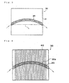
- the thickness of the filter films that are formed on the surfaces of the glass substrates 10 by the above-mentioned process has a concentric-circular distribution that is centered on the center of the substrate holder 2, so that a filter film 20 with good characteristics is formed in a more or less circular arc form pattern (in a bow shape) on the surface of each-glass substrate 10 (see Figure 3).
- the positions and shapes (more or less circular arc form shapes) of these filter films 20 with good characteristics are determined by measuring the spectroscopic transmissivity characteristics in lattice squares that are approximately 2 mm on a side for the entire region of the respective filter films formed on the glass substrates 10, preparing a map that connects portions having the same characteristics, and then analyzing the coordinate positions and curvature radii of the portions of the filter films that have good characteristics.
- a plurality of small filter member pieces 40, 40, ... constituting the required quantity of small filter member pieces are obtained by cutting the filter members 30 to the required dimensions in the direction perpendicular to the chord (line segment L indicated by a one-dot chain line in Figure 3) connecting both ends of the circular arc form portion of each filter film 20 having good characteristics as shown in Figure 4.
- 20a indicates the filter films with good characteristics in the small filter member pieces 40 thus obtained.
- FIG. 5 shows one example of a dicing saw 80 used to cut the above-mentioned filter members 30.
- This dicing saw 80 is a blade saw which has a blade 81 that is an ultra-thin circular blade, and is constructed so that the blade 81 is caused to rotate by driving a rotating shaft 82 by means of a motor (not shown in the figures).
- the diameter of the blade 81 is approximately 50 mm to 150 mm, and the thickness is approximately 0.03 mm to 2 mm.
- a blade that is used in most cases is a so-called metal-bond diamond blade using a material obtained by the mixed sintering of various type of metal powders consisting chiefly of bronze as a binder, or a so-called resin-bond diamond blade using a resin component such as a phenol resin or polyimide as a binder.
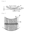
- the stage (base stand) 83 is a circular stand on whose upper surface the filter member 30 that is the object of cutting is placed; this stage 83 is free to rotate about a central axis AX that extends in the vertical direction, and can be moved horizontally in any desired direction.
- the filter member 30 is first bonded to a stage glass 84 by means of a hot-melt wax, and the stage glass 84 is then attached to the surface of the stage 83 by vacuum suction. Then, the rotating shaft 82 is driven so that the blade 81 is caused to rotate at approximately 30,000 rpm (this rpm is varied according to material of the blade 81 and the cutting conditions at the cutting surface of the fil ter member 30), and the stage 83 is caused to move at a feeding speed of approximately 1 to 5 mm/sec, so that the filter member 30 is cut.
- the system is adjusted so that the edge of the blade 81 cuts into the upper surface of the stage glass 84 to a depth of approximately 0.1 to 03 mm as shown in Figure 6 (the cut-in depth is indicated by d in Figure 6), and cutting is accomplished by downcutting with the feed direction of the stage 83, i.e., the base glass 84, set in the same direction as the direction of rotation of the blade 81.
- the filter member 30 is always placed on the stage 83 so that the filter film 20 (optical multi-layer film) is on the side of the upper surface (see Figure 6).
- the filter film 20 is positioned on the side-of the undersurface-(i.e., the side that contacts the base glass 84), the filter film 20 will peel and show relatively severe chipping and cracking when the blade 81 is caused to cut into the filter member 30.
- the filter member 30 is placed on the stage 83 so that the filter film 20 is positioned on the side of the upper surface, and the system is devised so that downcutting is performed, the above-mentioned chipping and peeling can be conspicuously reduced.
- an anti-reflection film etc.
- this anti-reflection film contacts the base glass 84.
- Such an anti-reflection film generally has a smaller thickness than the optical multi-layer film.
- filter films used in optical communications require extremely precise transmission (reflection) characteristics with respect to wavelength; accordingly, the total number of film layers required in order to satisfy such a requirement may reach several tens of layers.
- a few layers are sufficient in the case of an anti-reflection film; accordingly, the likelihood of peeling is much lower in the anti-reflection film than in the filter film. Accordingly, even if cutting is performed in such a state, there is little danger that chipping or peeling, etc., will occur in the anti-reflection film.
- the filter member 30 When the filter member 30 is thus cut into a plurality of small filter member pieces 40, 40, ..., an amount of glass equal to the thickness of the blade 81 of the dicing saw 80 is removed from the original glass substrate 10, so that gaps of a very small width are generated between the respective small filter member pieces 40, 40, ....
- the filter member 30 following cutting is heated so that the wax is softened, and the entire assembly of the small filter member pieces 40, 40, ... is compressed from both sides to produce a state in which such gaps are not generated.
- the small filter member pieces 40, 40, ... are rearranged so that the filter films 20a, 20a, ... with good characteristics in the small filter member pieces 40, 40, ... are lined up in a more or less rectilinear pattern as shown in Figure 7, and these small filter member pieces 40, 40, ... are then re-bonded by means of a hot-melt wax.
- This tool 101 consists of a plate-form member, each having a recessed part 101a on one side.
- the lower ends of the respective small filter member pieces 40, 40, ... that have been compressed as described above are caused to contact the recessed part 101a of the tool 101.
- the filter films 20a, 20a, ... following rearrangement will be lined up in a more or less rectilinear pattern.
- the new arc formed by the filter films 20a, 20a, ... present on the small filter member pieces 40, 40, ... in the state in which these small filter member pieces 40 are compressed as described above is not a circular arc like the initial arc, but is rather an elliptical arc; for practical purposes, however, this may be viewed as a circular arc.
- the plurality of tools 101 shown in Figure 8 consist of three tools 101 whose recessed parts 101a thus have different curvature radii. Furthermore, the "+" symbols in the figure indicate the positions of the centers of the curvature radii of the recessed parts 101a in the respective tools 101.
- the glass substrate 110 may be rectangular as long as this substrate is large enough to contain all of the annular filter film 120; however, it is desirable that this glass substrate 110 be a disk-form substrate as shown in Figure 12.
- the system is arranged so that the center of this disk more or less coincides with the center of the rotating shaft 3 of the substrate holder 2. Furthermore, it is advisable to form a hole H in the central portion, and to dispose a monitoring glass 111 that monitors the conditions of film formation in this position as shown in Figure 12. Furthermore, it is desirable that the thickness of the glass substrate 110 be greater than the final finished dimension. The reason for this is that there are cases in which warping occurs in the glass substrate 110 as a result of film stress in the filter film 120 formed on the glass substrate 110, and occurrence of such warping in the glass substrate 110 due to film formation can be prevented if such an approach is used. Furthermore, the glass substrate 110 can be adjusted to the desired thickness by planing following film formation.
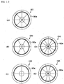
- the disk-form filter member 130 is first mounted on the stage 83 of the above-mentioned dicing saw 80 using a hot-melt wax or a commercially marketed UV sheet of the type used in the cutting of semiconductor wafers, etc., and this filter member 130 is cut into eight equal parts by means of the rotating blade 81 as shown in Figure 13 (A), thus producing new filter members 130a, 130a, ... (see Figure 14).
- the filter member 130 may also be cut into six, four, twelve or ten equal parts as shown in Figures 13 (B) through 13 (E).
- the system it is advisable to arrange the system so that new filter members 130a, 130a, ... that have the same shape are obtained. This is done so that the tool 201 that is used to rearrange the small filter member pieces 140, 140, ... (described later) can be used in common for all of the small filter member pieces 140, 140, .... Furthermore, the optimal number of parts into which the filter member 130 is divided depends on the radius of the annular filter film 120 and the dimensions of the glass substrate 110, etc.. Moreover, with consideration being given to the subsequent cutting and rearrangement of the small filter member pieces 140, 140, ..., either the outer circumferential portion or inner circumferential portion of the filter member 130 may be cut away to form the member into a rectilinear shape.
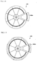
- the necessary number of small filter part members 140, 140, ... are obtained by cutting the filter member 130 in the direction perpendicular to the c hord that connects both ends of the circular arc form portion of the filter-film 120 with good characteristics as shown in Figure 16.
- dummy glasses 181 and 182 that have a more or less triangular shape (the approximate triangles ABC and A'B'C' shown in the figure) be attached to both the left and right side parts of the filter member 130.
- the filter member 130 following-this cutting is heated so that the hot-melt wax is softened, and the entire assembly of the small filter member pieces 140, 140, ... is compressed from both sides so that the cutting margin of the blade 81 caused by cutting is eliminated, thus producing a state in which the above-mentioned gaps are not generated.
- the small filter member pieces 140, 140, ... have been rearranged so that the filter films 120a, 120a, ... with good characteristics in the respective small filter member pieces 140, 140, ... are lined up in a more or less rectilinear pattern as shown in Figure 17, the small filter member pieces 140, 140, ... are re-bonded by means of the hot-melt wax.
- a tool 201 of the type shown in Figure 18 for the rearrangement of the above-mentioned small filter member pieces 140, 140, ....
- This tool 201 also consists of a plate-form member, and has a projecting part 201a on one side (the "+" symbol in Figure 18 indicates the center of the curvature radius of the projectin g part 201a of the tool 201). Then, for example, in order to rearrange the small filter member pieces 140, 140, ... shown in Figure 16 using such a tool 201, the lower ends of the respective compressed small filter member pieces 140, 140, ... are caused to contact the projecting part 201a of the tool 201.
- the filter films 120a, 120a, ... will be lined up in a more or less rectilinear pattern following rearrangement.
- the new arc formed by the filter films 120a, 120a,... present on the small filter member pieces 140, 140, ... in the above-mentioned compressed state is not a circular arc like the initial arc, but is rather an elliptical arc; for practical purposes, however, this may be viewed as a circular arc.
- filter chips 150, 150, ... can be cut out with good efficiency by effectively utilizing the filter film 120 with good characteristics that is formed in an annular shape.
- the filter member 130 is placed on the stage 83 so that the filter film 120 (optical multi-layer film) is on the side of the upper surface, and cutting is accomplished by downcutting using the dicing saw 80. In this way, chipping and peeling that accompany cutting can be conspicuously reduced as in the above-mentioned embodiment.
- a production process can be employed in which a filter member 30 (or 130) is manufactured by forming an optical multi-layer film on a glass substrate 10 (or 110), and then obtaining filter chips 50 (150) by cutting these chips out from this.filter member 30 (130). Accordingly, it is not absolutely necessary to use a working method in which optical multi -layer films are formed on glass substrates that have been cut out to specified dimensions beforehand as in conventional techniques, so that the productivity of the optical multi-layer films can be greatly improved.
- the glass substrate 110 on which the filter film 120 with good characteristics is formed in an annular shape need not necessarily be a disk-form substrate of the type described above (for example, a rectangular substrate may also be used); however, if the glass substrate 110 is a more or less disk-form substrate as described above, the waste glass portion that is cut away by the cutting process can be reduced from the outset, so that the manufacturing cost can be lowered.
- a blade saw was used to cut the filter members.
- the saw used to cut the filter members is not limited to a blade saw; some other cutting mechanism such as a wire saw may also be used.
- the above-mentioned cutting method used in cases where th e filter film is an optical multi-layer film is always effective not only in cases where cutting is performed for the purpose of obtaining filter chips from the filter member as described above, but also in cases where filter members are cut in which a filter film consisting of an optical multi-layer film is formed on one side of a glass substrate.
- the present invention can be used to manufacture optical filters containing optical multi-layer films with good productivity.
Landscapes
- Physics & Mathematics (AREA)
- General Physics & Mathematics (AREA)
- Optics & Photonics (AREA)
- Optical Filters (AREA)
- Processing Of Stones Or Stones Resemblance Materials (AREA)
- Liquid Crystal (AREA)
Abstract
Description
Claims (8)
- A filter member manufacturing method for obtaining a filter member by using a film forming apparatus in which a filter film that has desired characteristics is formed in an annular shape, and forming the above-mentioned filter film on a substrate, wherein the above-mentioned filter member is obtained by positioning a substrate throughout the entire region in which the above-mentioned filter film with desired characteristics is formed.
- A filter member cutting method for cutting a filter member in which a filter film consisting of an optical multi-layer film is formed on one side of a substrate, wherein this method comprises a step in which the above-mentioned filter member is placed on a base stand so that the above-mentioned filter film is on the upper surface of the filter member, and the above-mentioned filter member is cut by downcutting using a dicing saw.
- A filter member cutting method for cutting a filter member in which a filter film consisting of an optical multi-layer film is formed on one side of a substrate, and a film member with a smaller number of laminated layers than the above-mentioned filter film is formed on the other side of the above-mentioned substrate, wherein this method comprises a step in which the above-mentioned filter member is placed on a base stand so that the above-mentioned filter film is on the upper surface of the filter member, and the above-mentioned filter member is cut by downcutting using a dicing saw.
- A filter chip cut-out method for cutting out a plurality of filter chips from a filter member in which portions of a filter film formed on a substrate that have desired characteristics constitute a more or less circular arc form region, wherein this method comprises a first step in which a plurality of small filter member pieces are obtained by cutting the above-mentioned filter member in the direction perpendicular to the chord of the above -mentioned circular arc, a second step in which the above-mentioned plurality of small filter member pieces are rearranged so that the portions of the above-mentioned plurality of small filter member pieces that correspond to the above-mentioned circular arc form region are lined up in a more or less rectilinear pattern, and a third step in which a plurality of filter chips are obtained by cutting the above-mentioned rearranged plurality of small filter member pieces in the direction perpendicular to the direction of cutting in the above -mentioned first step.
- The filter chip cut-out method according to Claim 4, wherein the above-mentioned rearrangement of the above-mentioned small filter member pieces is performed in the above-mentioned second step using a tool which has a projecting or recessed part that has more or less the same curvature radius as the curvature radius in the above-mentioned circular arc form region.
- A filter chip manufacturing method comprising a first step in which a filter member is obtained using a film forming apparatus in which a filter film that has desired characteristics is formed in an annular shape, with a substrate being positioned throughout the entire region in which the above-mentioned filter film that has desired characteristics is formed, a second step in which the above-mentioned filter member including at least a portion of th e annular region constituting the above-mentioned filter film that has desired characteristics is cut through the center of the curvature radius of the above-mentioned annular region so that the filter member is divided into a plurality of filter members in which the above-mentioned filter film that has desired characteristics is present in more or less a circular arc form pattern, a third step in which a plurality of small filter member pieces are obtained by cutting the above-mentioned filter members obtained in theabove-mentioned second step in the durection perpendicular to the chord of the above-mentioned circular arc, a fourth step in which the above-mentioned plurality of small filter member pieces are rearranged so that the portions of the above-mentioned plurality of small filter member pieces that correspond to the above-mentioned circular arc form region are lined up in a more or less rectilinear pattern, and a fifth step in which a plurality of filter chips are obtained by cutting the above-mentioned rearranged plurality of small filter member pieces in the direction perpendicular to the cutting direction in the above -mentioned third step.
- The filter chip manufacturing method according to Claim 6, wherein the above-mentioned substrate has a more or less disk-form shape.
- The filter chip manufacturing method according to Claim 6 or Claim 7, wherein the above-mentioned rearrangement of the above-mentioned small filter member pieces is performed using a tool which has a projecting or recessed part that has more or less the same curvature radius as the curvature radius of the above-mentioned circular arc form region.
Applications Claiming Priority (3)
| Application Number | Priority Date | Filing Date | Title |
|---|---|---|---|
| JP2000308945A JP3590886B2 (en) | 2000-10-10 | 2000-10-10 | Method for manufacturing filter member, method for cutting filter member, method for cutting out filter chip, and method for manufacturing filter chip |
| JP2000308945 | 2000-10-10 | ||
| PCT/JP2001/007325 WO2002031545A1 (en) | 2000-10-10 | 2001-08-28 | Filter member manufacturing method, filter member cutting method, filter chip cutting method, and filter chip manufacturing method |
Publications (2)
| Publication Number | Publication Date |
|---|---|
| EP1327894A1 true EP1327894A1 (en) | 2003-07-16 |
| EP1327894A4 EP1327894A4 (en) | 2010-08-04 |
Family
ID=18789184
Family Applications (1)
| Application Number | Title | Priority Date | Filing Date |
|---|---|---|---|
| EP01958524A Withdrawn EP1327894A4 (en) | 2000-10-10 | 2001-08-28 | Filter member manufacturing method, filter member cutting method, filter chip cutting method, and filter chip manufacturing method |
Country Status (5)
| Country | Link |
|---|---|
| US (1) | US6979476B2 (en) |
| EP (1) | EP1327894A4 (en) |
| JP (1) | JP3590886B2 (en) |
| CA (1) | CA2415578C (en) |
| WO (1) | WO2002031545A1 (en) |
Families Citing this family (1)
| Publication number | Priority date | Publication date | Assignee | Title |
|---|---|---|---|---|
| KR20160032221A (en) * | 2013-07-18 | 2016-03-23 | 코닌클리케 필립스 엔.브이. | Dicing a wafer of light emitting devices |
Family Cites Families (8)
| Publication number | Priority date | Publication date | Assignee | Title |
|---|---|---|---|---|
| US2432950A (en) * | 1943-09-24 | 1947-12-16 | Bausch & Lomb | Apparatus for making optical wedges |
| FR2455751A1 (en) * | 1979-05-02 | 1980-11-28 | Thomson Csf | HIGH DYNAMIC MULTISPECTRAL OPTOELECTRIC RECEIVER SYSTEM |
| JPS5956577A (en) * | 1982-09-25 | 1984-04-02 | Matsushita Electric Ind Co Ltd | Vapor deposition method |
| FR2596529B1 (en) | 1986-03-28 | 1988-05-13 | Thomson Csf | OPTICAL WAVEGUIDE IN SEMICONDUCTOR MATERIAL, LASER APPLYING THE SAME AND WAVEGUIDE |
| JPS6360401A (en) * | 1986-09-01 | 1988-03-16 | Fujitsu Ltd | Manufacture of optical film parts |
| JPS63286568A (en) * | 1987-05-18 | 1988-11-24 | Canon Inc | Deposited film formation method |
| JPH09205071A (en) * | 1996-01-24 | 1997-08-05 | Hitachi Ltd | Dicing method and apparatus |
| JP3844886B2 (en) * | 1998-07-28 | 2006-11-15 | 富士通株式会社 | Manufacturing method of optical filter |
-
2000
- 2000-10-10 JP JP2000308945A patent/JP3590886B2/en not_active Expired - Lifetime
-
2001
- 2001-08-28 US US10/297,714 patent/US6979476B2/en not_active Expired - Fee Related
- 2001-08-28 EP EP01958524A patent/EP1327894A4/en not_active Withdrawn
- 2001-08-28 CA CA002415578A patent/CA2415578C/en not_active Expired - Lifetime
- 2001-08-28 WO PCT/JP2001/007325 patent/WO2002031545A1/en not_active Ceased
Also Published As
| Publication number | Publication date |
|---|---|
| US6979476B2 (en) | 2005-12-27 |
| EP1327894A4 (en) | 2010-08-04 |
| JP3590886B2 (en) | 2004-11-17 |
| JP2002116319A (en) | 2002-04-19 |
| CA2415578A1 (en) | 2003-01-09 |
| WO2002031545A1 (en) | 2002-04-18 |
| US20040021968A1 (en) | 2004-02-05 |
| CA2415578C (en) | 2006-12-05 |
Similar Documents
| Publication | Publication Date | Title |
|---|---|---|
| KR102065829B1 (en) | Substrate processing method | |
| CN100339974C (en) | Wafer processing method | |
| JP3904585B2 (en) | Manufacturing method of semiconductor device | |
| CN111029301B (en) | Processing method of silicon carbide-based wafer | |
| WO2009148073A1 (en) | Scribing wheel and method for scribing brittle material substrate | |
| KR20200007660A (en) | Method for processing led wafer | |
| JP2017118096A (en) | Substrate processing method | |
| CN101530011A (en) | Method for manufacturing metallized ceramic substrate chip | |
| TWI327340B (en) | Production method for semiconductor device | |
| JP2008147412A (en) | Semiconductor wafer, semiconductor device, semiconductor wafer manufacturing method, and semiconductor device manufacturing method | |
| KR20230114708A (en) | Method of manufacturing single crystal silicon substrate | |
| KR20230062378A (en) | Method for manufacturing a substrate | |
| JP2010142890A (en) | Method of correcting outer circumferential shape of cutting member, dresser board, and cutting device | |
| JPH04262589A (en) | Manufacture of optical semiconductor device | |
| US6979476B2 (en) | Filter member manufacturing method, filter member cutting method, filter chip cutting method, and filter chip manufacturing method | |
| CN112736034A (en) | Method for manufacturing ceramic chip | |
| CN113634878A (en) | Optical system and method for laser cutting multilayer materials | |
| CN111276577B (en) | Manufacturing method of LED chip | |
| KR20240005584A (en) | Substrate manufacturing method | |
| JP7764186B2 (en) | Substrate manufacturing method | |
| JP2020141009A (en) | Substrate material and laser processing method | |
| US7166487B2 (en) | Manufacturing method of optical devices | |
| JP7862229B2 (en) | Manufacturing method for single-crystal silicon substrates | |
| JPH11317384A (en) | Method of preparing end faces on integrated circuits | |
| JP2006203251A (en) | Production method for semiconductor device |
Legal Events
| Date | Code | Title | Description |
|---|---|---|---|
| PUAI | Public reference made under article 153(3) epc to a published international application that has entered the european phase |
Free format text: ORIGINAL CODE: 0009012 |
|
| 17P | Request for examination filed |
Effective date: 20030508 |
|
| AK | Designated contracting states |
Designated state(s): AT BE CH CY DE DK ES FI FR GB GR IE IT LI LU MC NL PT SE TR |
|
| RBV | Designated contracting states (corrected) |
Designated state(s): DE FR GB IT NL |
|
| RAP1 | Party data changed (applicant data changed or rights of an application transferred) |
Owner name: NIKON CORPORATION |
|
| A4 | Supplementary search report drawn up and despatched |
Effective date: 20100705 |
|
| RIC1 | Information provided on ipc code assigned before grant |
Ipc: C23C 14/08 20060101ALI20100629BHEP Ipc: C23C 14/00 20060101ALI20100629BHEP Ipc: G02B 5/28 20060101AFI20020419BHEP |
|
| STAA | Information on the status of an ep patent application or granted ep patent |
Free format text: STATUS: THE APPLICATION IS DEEMED TO BE WITHDRAWN |
|
| 18D | Application deemed to be withdrawn |
Effective date: 20100905 |