EP1326306A2 - Connecting member for flat circuit member and method of connecting the connecting member and the flat circuit member - Google Patents
Connecting member for flat circuit member and method of connecting the connecting member and the flat circuit member Download PDFInfo
- Publication number
- EP1326306A2 EP1326306A2 EP02102815A EP02102815A EP1326306A2 EP 1326306 A2 EP1326306 A2 EP 1326306A2 EP 02102815 A EP02102815 A EP 02102815A EP 02102815 A EP02102815 A EP 02102815A EP 1326306 A2 EP1326306 A2 EP 1326306A2
- Authority
- EP
- European Patent Office
- Prior art keywords
- flat circuit
- circuit member
- side wall
- connecting member
- claw
- Prior art date
- Legal status (The legal status is an assumption and is not a legal conclusion. Google has not performed a legal analysis and makes no representation as to the accuracy of the status listed.)
- Granted
Links
Images



Classifications
-
- H—ELECTRICITY
- H01—ELECTRIC ELEMENTS
- H01R—ELECTRICALLY-CONDUCTIVE CONNECTIONS; STRUCTURAL ASSOCIATIONS OF A PLURALITY OF MUTUALLY-INSULATED ELECTRICAL CONNECTING ELEMENTS; COUPLING DEVICES; CURRENT COLLECTORS
- H01R12/00—Structural associations of a plurality of mutually-insulated electrical connecting elements, specially adapted for printed circuits, e.g. printed circuit boards [PCB], flat or ribbon cables, or like generally planar structures, e.g. terminal strips, terminal blocks; Coupling devices specially adapted for printed circuits, flat or ribbon cables, or like generally planar structures; Terminals specially adapted for contact with, or insertion into, printed circuits, flat or ribbon cables, or like generally planar structures
- H01R12/50—Fixed connections
- H01R12/59—Fixed connections for flexible printed circuits, flat or ribbon cables or like structures
- H01R12/65—Fixed connections for flexible printed circuits, flat or ribbon cables or like structures characterised by the terminal
- H01R12/67—Fixed connections for flexible printed circuits, flat or ribbon cables or like structures characterised by the terminal insulation penetrating terminals
- H01R12/68—Fixed connections for flexible printed circuits, flat or ribbon cables or like structures characterised by the terminal insulation penetrating terminals comprising deformable portions
-
- H—ELECTRICITY
- H05—ELECTRIC TECHNIQUES NOT OTHERWISE PROVIDED FOR
- H05K—PRINTED CIRCUITS; CASINGS OR CONSTRUCTIONAL DETAILS OF ELECTRIC APPARATUS; MANUFACTURE OF ASSEMBLAGES OF ELECTRICAL COMPONENTS
- H05K3/00—Apparatus or processes for manufacturing printed circuits
- H05K3/30—Assembling printed circuits with electric components, e.g. with resistors
- H05K3/32—Assembling printed circuits with electric components, e.g. with resistors electrically connecting electric components or wires to printed circuits
- H05K3/325—Assembling printed circuits with electric components, e.g. with resistors electrically connecting electric components or wires to printed circuits by abutting or pinching; Mechanical auxiliary parts therefor
- H05K3/326—Assembling printed circuits with electric components, e.g. with resistors electrically connecting electric components or wires to printed circuits by abutting or pinching; Mechanical auxiliary parts therefor the printed circuit having integral resilient or deformable parts, e.g. tabs or parts of flexible circuits
-
- H—ELECTRICITY
- H01—ELECTRIC ELEMENTS
- H01R—ELECTRICALLY-CONDUCTIVE CONNECTIONS; STRUCTURAL ASSOCIATIONS OF A PLURALITY OF MUTUALLY-INSULATED ELECTRICAL CONNECTING ELEMENTS; COUPLING DEVICES; CURRENT COLLECTORS
- H01R43/00—Apparatus or processes specially adapted for manufacturing, assembling, maintaining, or repairing of line connectors or current collectors or for joining electric conductors
- H01R43/01—Apparatus or processes specially adapted for manufacturing, assembling, maintaining, or repairing of line connectors or current collectors or for joining electric conductors for connecting unstripped conductors to contact members having insulation cutting edges
-
- Y—GENERAL TAGGING OF NEW TECHNOLOGICAL DEVELOPMENTS; GENERAL TAGGING OF CROSS-SECTIONAL TECHNOLOGIES SPANNING OVER SEVERAL SECTIONS OF THE IPC; TECHNICAL SUBJECTS COVERED BY FORMER USPC CROSS-REFERENCE ART COLLECTIONS [XRACs] AND DIGESTS
- Y10—TECHNICAL SUBJECTS COVERED BY FORMER USPC
- Y10T—TECHNICAL SUBJECTS COVERED BY FORMER US CLASSIFICATION
- Y10T29/00—Metal working
- Y10T29/49—Method of mechanical manufacture
- Y10T29/49002—Electrical device making
- Y10T29/49117—Conductor or circuit manufacturing
- Y10T29/49124—On flat or curved insulated base, e.g., printed circuit, etc.
- Y10T29/49147—Assembling terminal to base
- Y10T29/49151—Assembling terminal to base by deforming or shaping
-
- Y—GENERAL TAGGING OF NEW TECHNOLOGICAL DEVELOPMENTS; GENERAL TAGGING OF CROSS-SECTIONAL TECHNOLOGIES SPANNING OVER SEVERAL SECTIONS OF THE IPC; TECHNICAL SUBJECTS COVERED BY FORMER USPC CROSS-REFERENCE ART COLLECTIONS [XRACs] AND DIGESTS
- Y10—TECHNICAL SUBJECTS COVERED BY FORMER USPC
- Y10T—TECHNICAL SUBJECTS COVERED BY FORMER US CLASSIFICATION
- Y10T29/00—Metal working
- Y10T29/49—Method of mechanical manufacture
- Y10T29/49002—Electrical device making
- Y10T29/49117—Conductor or circuit manufacturing
- Y10T29/49124—On flat or curved insulated base, e.g., printed circuit, etc.
- Y10T29/49147—Assembling terminal to base
- Y10T29/49151—Assembling terminal to base by deforming or shaping
- Y10T29/49153—Assembling terminal to base by deforming or shaping with shaping or forcing terminal into base aperture
-
- Y—GENERAL TAGGING OF NEW TECHNOLOGICAL DEVELOPMENTS; GENERAL TAGGING OF CROSS-SECTIONAL TECHNOLOGIES SPANNING OVER SEVERAL SECTIONS OF THE IPC; TECHNICAL SUBJECTS COVERED BY FORMER USPC CROSS-REFERENCE ART COLLECTIONS [XRACs] AND DIGESTS
- Y10—TECHNICAL SUBJECTS COVERED BY FORMER USPC
- Y10T—TECHNICAL SUBJECTS COVERED BY FORMER US CLASSIFICATION
- Y10T29/00—Metal working
- Y10T29/49—Method of mechanical manufacture
- Y10T29/49002—Electrical device making
- Y10T29/49117—Conductor or circuit manufacturing
- Y10T29/49174—Assembling terminal to elongated conductor
- Y10T29/49181—Assembling terminal to elongated conductor by deforming
-
- Y—GENERAL TAGGING OF NEW TECHNOLOGICAL DEVELOPMENTS; GENERAL TAGGING OF CROSS-SECTIONAL TECHNOLOGIES SPANNING OVER SEVERAL SECTIONS OF THE IPC; TECHNICAL SUBJECTS COVERED BY FORMER USPC CROSS-REFERENCE ART COLLECTIONS [XRACs] AND DIGESTS
- Y10—TECHNICAL SUBJECTS COVERED BY FORMER USPC
- Y10T—TECHNICAL SUBJECTS COVERED BY FORMER US CLASSIFICATION
- Y10T29/00—Metal working
- Y10T29/49—Method of mechanical manufacture
- Y10T29/49002—Electrical device making
- Y10T29/49117—Conductor or circuit manufacturing
- Y10T29/49204—Contact or terminal manufacturing
- Y10T29/49208—Contact or terminal manufacturing by assembling plural parts
-
- Y—GENERAL TAGGING OF NEW TECHNOLOGICAL DEVELOPMENTS; GENERAL TAGGING OF CROSS-SECTIONAL TECHNOLOGIES SPANNING OVER SEVERAL SECTIONS OF THE IPC; TECHNICAL SUBJECTS COVERED BY FORMER USPC CROSS-REFERENCE ART COLLECTIONS [XRACs] AND DIGESTS
- Y10—TECHNICAL SUBJECTS COVERED BY FORMER USPC
- Y10T—TECHNICAL SUBJECTS COVERED BY FORMER US CLASSIFICATION
- Y10T29/00—Metal working
- Y10T29/49—Method of mechanical manufacture
- Y10T29/49002—Electrical device making
- Y10T29/49117—Conductor or circuit manufacturing
- Y10T29/49204—Contact or terminal manufacturing
- Y10T29/49208—Contact or terminal manufacturing by assembling plural parts
- Y10T29/49218—Contact or terminal manufacturing by assembling plural parts with deforming
-
- Y—GENERAL TAGGING OF NEW TECHNOLOGICAL DEVELOPMENTS; GENERAL TAGGING OF CROSS-SECTIONAL TECHNOLOGIES SPANNING OVER SEVERAL SECTIONS OF THE IPC; TECHNICAL SUBJECTS COVERED BY FORMER USPC CROSS-REFERENCE ART COLLECTIONS [XRACs] AND DIGESTS
- Y10—TECHNICAL SUBJECTS COVERED BY FORMER USPC
- Y10T—TECHNICAL SUBJECTS COVERED BY FORMER US CLASSIFICATION
- Y10T29/00—Metal working
- Y10T29/49—Method of mechanical manufacture
- Y10T29/49826—Assembling or joining
- Y10T29/49833—Punching, piercing or reaming part by surface of second part
- Y10T29/49835—Punching, piercing or reaming part by surface of second part with shaping
-
- Y—GENERAL TAGGING OF NEW TECHNOLOGICAL DEVELOPMENTS; GENERAL TAGGING OF CROSS-SECTIONAL TECHNOLOGIES SPANNING OVER SEVERAL SECTIONS OF THE IPC; TECHNICAL SUBJECTS COVERED BY FORMER USPC CROSS-REFERENCE ART COLLECTIONS [XRACs] AND DIGESTS
- Y10—TECHNICAL SUBJECTS COVERED BY FORMER USPC
- Y10T—TECHNICAL SUBJECTS COVERED BY FORMER US CLASSIFICATION
- Y10T29/00—Metal working
- Y10T29/49—Method of mechanical manufacture
- Y10T29/49826—Assembling or joining
- Y10T29/49908—Joining by deforming
- Y10T29/49915—Overedge assembling of seated part
- Y10T29/49922—Overedge assembling of seated part by bending over projecting prongs
Definitions
- the present invention relates to a connecting member for a flat circuit member and a method of connecting the connecting member and the flat circuit member, and more particularly to a connecting member for a flat circuit member which can be electrically connected reliably to a conductor portion in a flat circuit member such as a flexible printed circuit (FPC), a flexible flat cable (FFC), and a ribbon cable as well as a method of connecting the same.
- a flat circuit member such as a flexible printed circuit (FPC), a flexible flat cable (FFC), and a ribbon cable as well as a method of connecting the same.
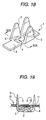
- Fig. 18 is a perspective view illustrating a connecting member (electric connection member) 1
- Fig. 19 is a cross-sectional view, taken in the direction of arrows along line XIX - XIX, of the connecting member 1 shown in Fig. 18 and illustrating the cross section of a flat circuit member (FFC) 10
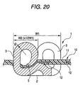
- Fig. 20 is an enlarged cross-sectional view illustrating a state in which the connecting member 1 is used.
- the connecting member 1 has a bottom plate portion (proximal portion) 2, a plurality of claw portions (crimping pieces) 3 rising from both side edges of the bottom plate portion 2 in the thickness direction, and an arcuate contact portion 4 provided projectingly on the bottom plate portion 2.
- the claw portions 3 of the connecting member 1 are caused to penetrate first piercing portions (portions of an insulating portion (insulating coating) 11 in Fig. 19) of the flat circuit member 10, as shown in Fig. 19. Subsequently, the claw portions 3 are bent toward the bottom plate portion 2 in such a manner as to clamp the flat circuit member 10 between the arcuate contact portion 4 on the bottom plate portion 2 and the claw portions 3. At this time, as shown in Fig.
- the insulating portion 11 of the flat circuit member 10 clamped between the claw portions 3 and a concave arcuate surface 5 formed in advance on the arcuate contact portion 4 is peeled off by distal edges of the claw portions 3.
- a conductor portion 12 of the flat circuit member 10 thereby exposed and the claw portions 3 of the connecting member 1 are brought into contact with each other, thereby electrically connecting the flat circuit member 10 and the connecting member 1.
- the width of the connecting member 1 is W1
- the bent width W2 of the claw portion 3 which is bent with a dimension of curl R becomes approximately one half of the just-mentioned width W1 of the connecting member 1 (i.e., W2 ⁇ W1 ⁇ 2).
- each connecting member 1 In a case where the interval between adjacent ones of the plurality of conductor portions 12 in the flat circuit member 10 is small and the width of each conductor portion 12 is narrow, each connecting member 1 must be made compact correspondingly. However, in conjunction with this miniaturization, the width W1 of the connecting member 1 becomes narrow, and therefore the dimension of curl R of the claw portion 3 must also be made small. In such a connecting member 1, there is a possibility that it becomes difficult to bend the claw portion 3 smoothly. In addition, since the width W1 of the connecting member 1 becomes narrow (i.e., the width of the bottom plate portion 2 becomes narrow), it becomes difficult to form the arcuate contact portion 4 on the bottom plate portion 2.
- the invention has been made in view of the above-described problems, and its object is to provide a connecting member for a flat circuit member which can be electrically connected reliably to a conductor portion in a flat circuit member and can ensure stable connection even in a case where the interval between adjacent ones of a plurality of conductor portions in the flat circuit member is small and the width of each conductor portion is narrows as well as a method of connecting the connecting member and the flat circuit member.
- the invention is characterized by having the following arrangement.
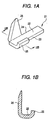
- Fig. 1A is a perspective view illustrating the configuration of a connecting member 21 in accordance with a first embodiment of the invention
- Fig. 1B is a cross-sectional view taken in the direction of arrows along line IIB - IIB in Fig. 1A.
- the whole of the connecting member 21 is integrally formed by subjecting an appropriate electrically conductive metal plate to press forming
- the connecting member 21 has a bottom plate portion 22, a side wall portion 25 extending upward from a widthwise side edge 23 of the bottom plate portion 22 substantially in parallel with the thickness direction of the bottom plate portion 22, and a claw portion 26 extending upward from the other side 24 of the bottom plate portion 22 substantially in parallel with the thickness direction of the bottom plate portion 22 in such a manner as to oppose the side wall portion 25.
- the claw portion 26 is tapered.
- Figs. 2A and 2B illustrate an example of the flat circuit member.
- Fig. 2A is a partially cutaway view of a flat circuit member 100
- Fig. 2B is a partially cutaway view of a flat circuit member 110.
- the flat circuit member 100 shown in Fig. 2A has thick conductor portions 102, whereas the flat circuit member 110 shown in Fig. 2B has thin conductor portions 112. Further, in the flat circuit member 100, each conductor portion 102 is covered with an insulating portion 101 and is insulated from the outside, whereas in the flat circuit member 110 each conductor portion 112 is formed on an insulating portion 111. It should be noted, however, that the flat circuit member which is connected to the connecting member of the invention is not limited to the flat circuit member 100 and the flat circuit member 110. Namely, it should be construed that there are various forms in the configuration of the flat circuit member, the circuit pattern of the conductor portions formed in or on the flat circuit member, and so forth.
- the thick conductor portions 102 may be formed on the insulating portion as in the flat circuit member 110 shown in Fig. 2B.
- the flat circuit member which is connected to the connecting member of the invention may adopt a form in which the conductor portions are partially exposed from the insulating portion in various forms.
- the connecting member 21 When the connecting member 21 is connected to the flat circuit member, the connecting member 21 is first positioned below the flat circuit member, and the claw portion 26 is subsequently caused to penetrate a first piercing portion of the flat circuit member in the thickness direction thereof.
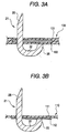
- Fig. 3A shows a state in which the connecting member 21 has penetrated a first piercing portion (in this example, a portion where the conductor portion and the insulating portion are present) of the flat circuit member 100
- Fig. 3B shows a state in which the connecting member 21 has penetrated a first piercing portion (in this example, a portion where the conductor portion and the insulating portion are present) of the flat circuit member 110.
- Fig. 3B shows an example in which the claw portion 26 has penetrated the flat circuit member 110 while the conductor portion 112 exposed on the flat circuit member 110 is oriented toward the bottom plate portion 22 of the connecting member 21.
- the first piercing portion of the flat circuit member which is penetrated by the claw portion 26 of the connecting member 21, may include both the insulating portion and the conductor portion, as shown in Figs. 3A and 3B, but the first piercing portion may not necessarily include the conductor portion. Namely, it is not necessarily essential for the portion of the flat circuit member where the conductor portion is present to be penetrated by the claw portion 26 of the connecting member 21, and the portion of the flat circuit member where only the insulating portion is present may be penetrated in the thickness direction thereof. However, consideration should be given to the fact that a greater number of electric contacts are obtained as the claw portion 26 penetrates the conductor portion and is brought into contact with the cross section of the conductor portion. Of course, the portion of the flat circuit member where only the conductor portion is present may be penetrated in the thickness direction thereof.
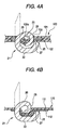
- the claw portion 26 is bent toward the bottom plate portion 22 such that a distal end portion of the claw portion 26 pierces a second piercing portion 103 of the flat circuit member 100 which is different from the aforementioned first piercing portion of the flat circuit member 100.
- the claw portion 26 is particularly bent such that the distal end portion of the claw portion 26 pierces the conductor portion 102. Consequently, a portion 102a of the conductor portion 102 located on the inner side of the bent claw portion 26 is clamped by an inner surface 29 of the claw portion 26, thereby making it possible to obtain electric contact between the cross section of the conductor portion 102 and the inner surface 29 of the claw portion 26.
- the portion 102a is clamped by the inner surface 29 of the claw portion 26 such that the portion 102a of the conductor portion 102 located on the inner side of the bent claw portion 26 becomes strained (i.e., deflected), the force for holding the contact between the cross section of the conductor portion 102 and the inner surface 29 of the claw portion 26 is generated or increased, thereby making it possible to obtain much more stable electric contact between the connecting member 21 and the flat circuit member 100.
- the side wall portion 25 forms a space between the bottom plate portion 22 and the flat circuit member 100 in cooperation with the bottom plate portion 22, as shown in Fig. 4A.
- the side wall portion 25 partially supports the bottom surface of the flat circuit member 100, and the second piercing portion 103 of the flat circuit member 100 is located in the vicinity of the side wall portion 25. This facilitates the piercing of the distal end portion of the claw portion 26 into the second piercing portion 103 of the flat circuit member 100.
- the claw portion 26 is bent toward the bottom plate portion 22 such that the flat circuit member 110 is clamped between an outer surface 28 of the claw portion 26 and an inner edge portion 27 of the side wall portion 25.
- the conductor portion 112 of the flat circuit member 110 is partially urged against the inner edge portion 27 of the side wall portion 25 by the urging force of the claw portion 26, and the portion of the conductor portion 112 abuts against the inner edge portion 27 of the side wall portion 25, thereby making it possible to obtain stable electric contact between the connecting member 21 and the flat circuit member 110.
- the side wall portion 25 acts to clamp the flat circuit member 110 in cooperation with the claw portion 26.
- the method of connecting the connecting member 21 to the flat circuit member has been described separately with respect to the two examples, either connecting method should be selected appropriately in the actual connection by studying and taking into consideration the thickness, flexibility, and the like of the flat circuit member which is actually used.
- the flat circuit member 110 having the thin conductor portions 102 is deflected greatly toward the bottom plate portion 22, as shown in Fig. 4B, since it has higher flexibility than the flat circuit member 100 having the thick conductor portions 102. Accordingly, in the case where the flat circuit member 110 is used, stable electric contact can be easily obtained by partially pressing the conductor portion against the side wall portion 25 by the claw portion 26 rather than by causing the claw portion 26 to pierce the conductor portion so as to obtain electric contact, as shown in Fig. 4A.
- a tensile force or a pressing force maybe applied, as required, to the flat circuit member from a direction substantially horizontal to the direction of extension of the flat circuit member.
- the position of the connecting member 21 may be moved, as required.
- the flat circuit member 110 is easily brought into contact with the upper surface (inner surface) of the bottom plate portion 22 as well, and if the conductor portion 112 is partially pressed against the bottom plate portion 22 as well by the distal end portion of the claw portion 26, it is possible to obtain further electric contact between the connecting member 21 and the conductor portion 112.
- the conductor portion 112 of the flat circuit member 110 may be mounted in such a manner as to race the bottom plate portion 22 of the connecting member 21, but the insulating portion 111 of the flat circuit member 110 may be mounted in such a manner as to face the bottom plate portion 22.
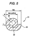
- the bent width W4 of the claw portion 26 which is bent with a dimension of curl R' becomes approximately equal to a value which is obtained by subtracting the thickness t of the connecting member 21 from the just-mentioned width W3 (i.e., W4 ⁇ W3 - t),
- the dimension of curl R' of the connecting member 21 can be set to be greater than the dimension of curl R of the connecting member 1 (i.e., R' > R). Namely, since leeway is provided in the range of the setting of the dimension of curl R', smooth curling of the claw portions becomes possible. Since there is leeway in the range of the setting of the dimension of curl R', in the invention the width W3 of the connecting member 21 can be made small by making the dimension of curl R' small.
- the claw portion 26 is bent such that the inner surface 29 and the outer surface 28 of the claw portion 26 is located on the inner side of the side wall portion 25.
- the claw portion 26 may be bent such that the inner surface 29 of the claw portion 26 is located as close to the vicinity of the outer surface of the side wall portion 25 as possible.
- the connecting member of the invention is applicable to various uses.
- the connecting member can be directly soldered to a mating member to be connected to, such as an electric circuit board and various devices, thereby making it possible to connect the flat circuit member to the mating member to be connected to.
- the bottom plate portion of the connecting member may be modified appropriately as to be used as a portion for soldering.
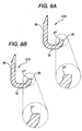
- Figs. 6A and 6B show a first modification of the connecting member 21 shown in Fig. 1, and specifically illustrate an example in which the inner edge portion 27 of the side wall portion 25 has been chamfered.
- Fig. 6A shows a connecting member 21A in which a curved surface 27' has been formed on the inner edge portion of the side wall portion 25, while Fig. 6B shows a connecting member 21B in which an inclined surface 27" has been formed on the inner edge portion of the side wall portion 25.
- the curved surface 27' or the inclined surface 27" is formed on the connecting member shown in Fig. 4A, it is possible to reliably prevent damage to the insulating portion 101 of the flat circuit member 100. Furthermore, when the claw portion 26 is bent toward the bottom plate portion 22 such that the distal end portion of the claw portion 26 pierces the conductor portion 102 of the flat circuit member 100, it becomes difficult for the flat circuit member 100 to resist the stress whereby it is pulled toward the proximal side of the claw portion 26. For this reason, the flat circuit member 100 is likely to slide on the curved surface 27' or the inclined surface 27", so that a strain is likely produced in the portion 102a of the conductor portion 102 located on the inner side of the bent claw portion 26.
- the curved surface 27' or the inclined surface 27" is formed on the connecting member shown in Fig. 4B, it is possible to reliably prevent damage to or cutting of the conductor portion 112 of the flat circuit member 110. Furthermore, when the claw portion 26 is bent toward the bottom plate portion 22 such that the flat circuit member 110 is clamped between the outer surface 28 of the claw portion 26 and the curved surface 27' or the inclined surface 27" of the side wall portion 25, it becomes difficult for the flat circuit member 110 to resist the stress whereby it is pulled toward the proximal side of the claw portion 26, and the flat circuit member 110 is capable of sliding smoothly on the curved surface 27' or the inclined surface 27". For this reason, the flat circuit member 110 having higher flexibility than the flat circuit member 100 shown in Fig.
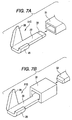
- Figs. 7A and 7B show a second modification of the connecting member 21 shown in Fig. 1.
- Fig. 7A shows a connecting member 21C in which a male terminal portion 30 connectable to a mating female terminal 31 is formed at one longitudinal end portion of the bottom plate portion 22 shown in Fig. 1.
- Fig. 7B shows a connecting member 21D in which a female terminal portion 32 connectable to a mating male terminal 33 is formed at one longitudinal end portion of that bottom plate portion 22.
- the flat circuit member having such a modified connecting member connected thereto is easily connected to another device having a mating terminal, and the range of application of the flat circuit member becomes wide.
- each of the male terminal portion 30 and the female terminal portion 32 maybe formed integrally with the connecting member or may be formed separately. However, they should preferably be formed integrally for the purpose of the lowering of the manufacturing cost through a decrease in the number of device parts of the connecting member and for the purpose of the improvement of strength. It goes without saying that the application of the first modification to this second modification is also effective.
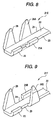
- Fig. 8 shows a third modification of the connecting member 21 shown in Fig. 1, and specifically shows a connecting member 21E which is provided with a plurality of claw portions and a plurality of side wall portions.
- a second side wall portion 25A extending upward from one side edge 23 of the bottom plate portion 22 substantially in parallel with the thickness direction of the bottom plate portion 22, as well as a second claw portion 26A extending upward from the other side edge 24 of the bottom plate portion 22 substantially in parallel with the thickness direction of the bottom plate portion 22 in such a manner as to oppose the side wall portion 25A, are further formed on the connecting member 21E in addition to the configuration of the connecting member shown in Fig. 1.
- connecting member 21E since electric contact with the conductor portion of the flat circuit member is formed at least at two portions, the reliability of electric contact improves.
- the connecting member 21E is effective in a case where a shortcircuiting circuit is formed for two independent conductor portions. It goes without saying that the application of the first modification and the second modification to this third modification is also effective.
- a slit or a recessed portion may not be formed between the side wall portion 25 and the second side wall portion 25A as shown by the dotted lines in Fig. 8, and these side wall portions may be formed continuously without a break.
- the side wall portion which is thus formed continuously without a break is preferable since its strength improves as compared with the case where the side wall portion 25 and the second side wall portion 25A are formed individually independently.
- Fig. 9 shows a fourth modification of the connecting member 21 shown in Fig. 1, and specifically shows a connecting member 21F which is provided with a plurality of claw portions and a plurality of side wall portions, but the positions where the second claw portion and the second side wall portion are formed differ in comparison with the connecting member 21E shown in Fig 8.
- a second side wall portion 25B extending upward from the other side edge 24 of the bottom plate portion 22 substantially in parallel with the thickness direction of the bottom plate portion 22, as well as a second claw portion 26B extending upward from one side edge 23 of the bottom plate portion 22 substantially in parallel with the thickness direction of the bottom plate portion 22 in such a manner as to oppose the inner surface of the side wall portion 25B, are further formed on the connecting member 21F in addition to the configuration of the connecting member shown in Fig. 1.
- connecting member 21F in the same way as the connecting member 21E shown in Fig. 8, since electric contact with the conductor portion of the flat circuit member is formed at least at two portions, the reliability of electric contact improves.
- the connecting member 21F is effective in a case where a shortcircuiting circuit is formed for two independent conductor portions. It goes without saying that the application of the first to third modifications to this fourth modification is also effective.
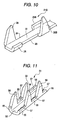
- Fig. 10 shows a fifth modification of the connecting member 21 shown in Fig. 1, and specifically shows a connecting member 21G which is provided with a plurality of claw portions and a plurality of side wall portions.
- the second claw portion 26B and the second side wall portion 25B are respectively provided at positions further spaced apart from the side wall portion 25 and the claw portion 26 in the longitudinal direction of the bottom plate portion 22.
- Fig. 11 is a perspective view illustrating the configuration of a connecting member 51 in accordance with a second embodiment of the invention.
- Fig. 12 is a side elevational view taken in the longitudinal direction of the connecting member 51 shown in Fig. 11.
- Fig. 13 is a top view of the connecting member 51 shown in Fig. 11.
- Fig. 14 is a cross-sectional view taken in the direction of arrows along line XIV - XIV in Fig. 13.
- Fig. 15 is a cross-sectional view taken in the direction of arrows along line XV - XV in Fig. 13.
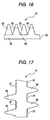
- Fig. 16 is a side elevational view taken in the widthwise direction of the connecting member 51 shown in Fig. 11.
- Fig. 17 is a development view of the connecting member 51 shown in Fig. 11.
- the whole of the connecting member 51 is integrally formed by subjecting an appropriate electrically conductive metal plate to press forming.
- the connecting member 51 is an embodiment of the modification of the first embodiment by taking into consideration the above-described first to fifth modifications.
- a plurality of wide wall portions 55 respectively extend upward from both widthwise side edges of a bottom plate portion 52 substantially in parallel with the thickness direction of the bottom plate portion 52, and a plurality of claw portions 56 respectively extend from both widthwise side edges of the bottom plate portion 52 in such a manner as to respectively oppose the plurality of side wall portions 55.
- the plurality of side wall portions 55 and the plurality of claw portions 56 are respectively arranged alternately (i.e., in a staggered manner) on both side edges of the bottom plate portion 52 along the longitudinal direction of the bottom plate portion 52.
- a slit or a recessed portion is not provided between each of the plurality of side wall portions 55 and each of the plurality of claw portions 56 which are juxtaposed alternately at each side edge of the bottom plate portion 52, and the side wall portions 55 and the claw portions 56 are formed continuously.
- the structure of the connecting member 51 is simplified, as shown in Figs. 16 and 17, for example. It is effective to apply these peculiar structures of the second embodiment to the first embodiment and the first to fifth modifications.
- the inner edge portions of the respective side wall portions 55 are chamfered, and curved surfaces or inclined surfaces 57 are formed thereon.
- connection between the connecting member 51 and the flat circuit member can be readily surmised from the details of the first embodiment described with reference to Figs. 1A to 6B, so that a description thereof will be omitted.
- operation and the like based on the configuration of the connecting member 51 can also be readily surmised from the description of the above-described first embodiment and various modifications, so that a description thereof will be omitted.
- each of the above-described connecting members may be formed integrally by welding, an electrically conductive adhesive agent, or the like after being respectively formed separately insofar as they are made of appropriate metals which are electrically conductive.
Landscapes
- Engineering & Computer Science (AREA)
- Metallurgy (AREA)
- Manufacturing & Machinery (AREA)
- Microelectronics & Electronic Packaging (AREA)
- Multi-Conductor Connections (AREA)
- Coupling Device And Connection With Printed Circuit (AREA)
- Combinations Of Printed Boards (AREA)
Abstract
Description
wherein the side wall portion supports the flat circuit member, and
wherein the second piercing portion is located in a vicinity of the side wall portion.
wherein the claw portion is bent such that a portion of the flat circuit member is clamped between an outer surface of the claw portion and an inner edge portion of the side wall portion so as to obtain electric contact with the conductor portion.
Claims (7)
- A connecting member for a flexible flat circuit member, comprising:wherein the claw portion penetrates a first piercing portion of the flat circuit member having a conductor portion in a thickness direction of the flat circuit member, and the claw portion is bent so that a distal end portion of the claw portion pierces a second piercing portion of the flat circuit member which is different from the first piercing portion so as to obtain electric contact with the conductor portion,a bottom plate portion;at least one side wall portion extending upward from one side edge of the bottom plate portions andat least one claw portion extending from the other side edge of the bottom plate portion so as to oppose to the side wall portion,
wherein the side wall portion supports the flat circuit member, and
wherein the second piercing portion is located in a vicinity of the side wall portion - The connecting member according to claim 1, wherein an edge portion of the side wall portion is chamfered.
- The connecting member according to claim 1, wherein the side wall portion partially supports the flat circuit member.
- The connecting member for a flat circuit member, comprising:wherein the claw portion penetrates a portion of the flat circuit member having a conductor portion in a thickness direction of the flat circuit member, anda bottom plate portion;at least one side wall portion extending upward from one side edge of the bottom plate portions andat least one claw portion extending from the other side edge of the bottom plate portion so as to oppose to the side wall portion,
wherein the claw portion is bent such that a portion of the flat circuit member is clamped between an outer surface of the claw portion and an inner edge portion of the side wall portion so as to obtain electric contact with the conductor portion. - The connecting member according to claim 4, wherein the inner edge portion of the side wall portion is chamfered.
- A method of connecting a connector member to a flat circuit member including a conductor portion, wherein the connecting member includes a bottom plate portion, at least one side wall portion extending upward from one side edge of the bottom plate portion, and at least one claw portion extending from the other side edge of the bottom plate portion so as to oppose to the side wall portion, the method comprising the steps of:wherein the side wall portion supports the flat circuit member, and the second piercing portion is located in a vicinity of the side wall portion.causing the claw portion to penetrate a first piercing portion of the flat circuit member in a thickness direction of the flat circuit member; andbending the claw portion such that a distal end portion of the claw portion pierces a second piercing portion of the flat circuit member which is different from the first piercing portion of the flat circuit member, so as to obtain electric contact with the conductor portion,
- A method of connecting a connecting member to a flat circuit member including a conductor member, wherein the connecting member includes a bottom plate portion, at least one side wall portion extending upward from one side edge of the bottom plate portion, and at least one claw portion extending from the other side edge of the bottom plate portion so as to oppose to the side wall portion, the method comprising the steps of:causing the claw portion to penetrate a portion of the flat circuit member in a thickness direction of the flat circuit member; andbending the claw portion such that a portion of the flat circuit member is clamped between an outer surface of the claw portion and an inner edge portion of the side wall portion, so as to obtain electric contact with the conductor portion.
Priority Applications (1)
| Application Number | Priority Date | Filing Date | Title |
|---|---|---|---|
| EP06112356A EP1691452A3 (en) | 2002-12-18 | 2002-12-18 | Connecting member for flat circuit member and method of connecting the connecting member and the flat circuit member |
Applications Claiming Priority (2)
| Application Number | Priority Date | Filing Date | Title |
|---|---|---|---|
| JP2001386320 | 2001-12-19 | ||
| JP2001386320A JP2003187892A (en) | 2001-12-19 | 2001-12-19 | Connecting member for flat circuit body and method for connecting the connecting member to flat circuit body |
Related Child Applications (1)
| Application Number | Title | Priority Date | Filing Date |
|---|---|---|---|
| EP06112356A Division EP1691452A3 (en) | 2002-12-18 | 2002-12-18 | Connecting member for flat circuit member and method of connecting the connecting member and the flat circuit member |
Publications (3)
| Publication Number | Publication Date |
|---|---|
| EP1326306A2 true EP1326306A2 (en) | 2003-07-09 |
| EP1326306A3 EP1326306A3 (en) | 2004-04-28 |
| EP1326306B1 EP1326306B1 (en) | 2006-08-23 |
Family
ID=19187935
Family Applications (1)
| Application Number | Title | Priority Date | Filing Date |
|---|---|---|---|
| EP02102815A Expired - Lifetime EP1326306B1 (en) | 2001-12-19 | 2002-12-18 | Connecting member for flat circuit member and method of connecting the connecting member and the flat circuit member |
Country Status (4)
| Country | Link |
|---|---|
| US (2) | US6652310B2 (en) |
| EP (1) | EP1326306B1 (en) |
| JP (1) | JP2003187892A (en) |
| DE (1) | DE60214122T2 (en) |
Families Citing this family (19)
| Publication number | Priority date | Publication date | Assignee | Title |
|---|---|---|---|---|
| EP1261081B1 (en) * | 2001-05-21 | 2010-03-17 | The Furukawa Electric Co., Ltd. | Method for assembling for flat cable connector and determining its connecting state |
| JP4115399B2 (en) * | 2003-08-06 | 2008-07-09 | 古河電気工業株式会社 | Connection method and connection structure between flat circuit body connector and flat circuit body |
| JP4536486B2 (en) * | 2004-11-04 | 2010-09-01 | 矢崎総業株式会社 | Piercing terminal and connection structure using piercing terminal |
| JP4839014B2 (en) * | 2005-04-07 | 2011-12-14 | 矢崎総業株式会社 | Manufacturing method of flat circuit body with terminal fitting, manufacturing mold of flat circuit body with terminal fitting, and manufacturing apparatus of flat circuit body with terminal fitting |
| JP2006310007A (en) * | 2005-04-27 | 2006-11-09 | Yazaki Corp | Wire harness assembly method, wire harness and connector |
| JP4509866B2 (en) * | 2005-06-03 | 2010-07-21 | 矢崎総業株式会社 | Terminal fitting |
| US7410384B2 (en) * | 2006-05-16 | 2008-08-12 | Fci Americas Technology, Inc. | Electrical contact with stapled connection |
| US20090170379A1 (en) * | 2007-12-28 | 2009-07-02 | Allina Jr Stanley F | Clip for connection to a stab terminal of an electrical buss and associated methods |
| USD630495S1 (en) * | 2007-12-28 | 2011-01-11 | Meter-Treater, Inc. | Clip for connection to a stab terminal of an electrical buss |
| USD630496S1 (en) * | 2007-12-28 | 2011-01-11 | Meter-Treater, Inc. | Clip for connection to a stab terminal of an electrical buss |
| US7686642B2 (en) | 2008-03-03 | 2010-03-30 | Tempo Industries, Inc. | Wire harness interconnection and retention method and apparatus |
| JP5465577B2 (en) * | 2010-03-31 | 2014-04-09 | 株式会社フジクラ | Crimp terminal |
| JP5465579B2 (en) * | 2010-03-31 | 2014-04-09 | 株式会社フジクラ | Crimp terminal |
| DE102011090184A1 (en) * | 2011-12-30 | 2013-07-04 | Siemens Aktiengesellschaft | Connecting device for electrical machines |
| JP6569127B2 (en) * | 2016-02-02 | 2019-09-04 | 株式会社オートネットワーク技術研究所 | Fixing structure between metal plate and synthetic resin material, and wiring member having the same |
| JP6780535B2 (en) * | 2017-02-22 | 2020-11-04 | 株式会社オートネットワーク技術研究所 | Wire harness |
| JP7232073B2 (en) * | 2019-02-18 | 2023-03-02 | 日本航空電子工業株式会社 | Connection method, connection structure and connection terminal |
| FR3099005B1 (en) * | 2019-07-18 | 2023-07-28 | Valeo Systemes Thermiques | Metallic electrical connector for flexible electrical conductive strip and associated connector conductive strip assembly |
| JP7717516B2 (en) * | 2021-07-26 | 2025-08-04 | メクテック株式会社 | Flexible printed wiring board with connection terminals and method for manufacturing the same |
Family Cites Families (11)
| Publication number | Priority date | Publication date | Assignee | Title |
|---|---|---|---|---|
| US3395381A (en) * | 1966-11-25 | 1968-07-30 | Amp Inc | Crimpable connecting device for flat conductor cable |
| GB1287865A (en) * | 1970-06-30 | 1972-09-06 | ||
| US3845456A (en) * | 1971-09-28 | 1974-10-29 | Molex Inc | Clinchable terminals |
| GB1474249A (en) * | 1974-01-09 | 1977-05-18 | Amp Inc | Electrical contact for flat conductor cable |
| US4066319A (en) * | 1974-04-30 | 1978-01-03 | Elco Corporation | Method and apparatus for flat conductor cable termination |
| US3924917A (en) * | 1974-04-30 | 1975-12-09 | Elco Corp | Flat cable termination method and apparatus |
| US4002393A (en) | 1974-12-05 | 1977-01-11 | Amp Incorporated | Contact means for flat conductor cable and method of connecting same |
| JPH048372A (en) | 1990-04-26 | 1992-01-13 | Mitsubishi Electric Corp | Radiation generation device |
| JPH0747810Y2 (en) | 1990-05-09 | 1995-11-01 | 住友電装株式会社 | Electrical connector for flexible flat conductor cable |
| JP3756938B2 (en) * | 1997-11-13 | 2006-03-22 | 古河電気工業株式会社 | Electrical connection terminal |
| DE19918340A1 (en) * | 1998-04-23 | 1999-10-28 | Whitaker Corp | Electrical terminal clip for connecting film and conductive tracks |
-
2001
- 2001-12-19 JP JP2001386320A patent/JP2003187892A/en active Pending
-
2002
- 2002-12-18 US US10/321,803 patent/US6652310B2/en not_active Expired - Fee Related
- 2002-12-18 EP EP02102815A patent/EP1326306B1/en not_active Expired - Lifetime
- 2002-12-18 DE DE60214122T patent/DE60214122T2/en not_active Expired - Lifetime
-
2003
- 2003-06-17 US US10/462,684 patent/US7047636B2/en not_active Expired - Fee Related
Also Published As
| Publication number | Publication date |
|---|---|
| DE60214122D1 (en) | 2006-10-05 |
| US20030114041A1 (en) | 2003-06-19 |
| EP1326306A3 (en) | 2004-04-28 |
| DE60214122T2 (en) | 2006-12-28 |
| JP2003187892A (en) | 2003-07-04 |
| EP1326306B1 (en) | 2006-08-23 |
| US20030232534A1 (en) | 2003-12-18 |
| US7047636B2 (en) | 2006-05-23 |
| US6652310B2 (en) | 2003-11-25 |
Similar Documents
| Publication | Publication Date | Title |
|---|---|---|
| US6652310B2 (en) | Connecting member for flat circuit member and method of connecting the connecting member and the flat circuit member | |
| EP0286422B1 (en) | Electrical connector terminal for a flexible printed circuit board | |
| EP1628366B1 (en) | Electric connector | |
| US6312283B1 (en) | Method of connecting terminal fitting to flat conductor and terminal fitting for flat conductor | |
| JP3734138B2 (en) | Flat cable terminal | |
| EP1237228A2 (en) | Relay connector | |
| JP3756938B2 (en) | Electrical connection terminal | |
| JP4101446B2 (en) | Electrical connection terminal | |
| EP1691452A2 (en) | Connecting member for flat circuit member and method of connecting the connecting member and the flat circuit member | |
| JP3852920B2 (en) | Piercing terminal connection structure | |
| JPH09213388A (en) | Wire harness and method of connecting printed circuit board and wire in wire harness | |
| US6332805B2 (en) | Structure for connecting flat circuit member | |
| EP1662615A2 (en) | Electric connector | |
| US20250062555A1 (en) | Electrical Connection Terminal and Electrical Connection Assembly | |
| JP2005141984A (en) | Piercing contact, flat cable with piercing contact, flat cable with connector, and method of manufacturing the same | |
| JPH0625897Y2 (en) | Conductive terminal | |
| JP3923318B2 (en) | Connection part between flat cable and wiring circuit body and connecting method between flat cable and wiring circuit body | |
| JP3933646B2 (en) | Connection between electrical connection terminal and flat cable | |
| JP3979487B2 (en) | Piercing terminal connection structure | |
| JP2002208451A (en) | Crimp terminal | |
| JP3285519B2 (en) | IDC electrical connector | |
| JP3269809B2 (en) | IDC electrical connector | |
| JPH0716302Y2 (en) | Electrical connection terminal | |
| JP2000182681A (en) | Flat cable connector | |
| JP2003115339A (en) | Piercing terminal |
Legal Events
| Date | Code | Title | Description |
|---|---|---|---|
| PUAI | Public reference made under article 153(3) epc to a published international application that has entered the european phase |
Free format text: ORIGINAL CODE: 0009012 |
|
| AK | Designated contracting states |
Designated state(s): AT BE BG CH CY CZ DE DK EE ES FI FR GB GR IE IT LI LU MC NL PT SE SI SK TR |
|
| AX | Request for extension of the european patent |
Extension state: AL LT LV MK RO |
|
| PUAL | Search report despatched |
Free format text: ORIGINAL CODE: 0009013 |
|
| AK | Designated contracting states |
Kind code of ref document: A3 Designated state(s): AT BE BG CH CY CZ DE DK EE ES FI FR GB GR IE IT LI LU MC NL PT SE SI SK TR |
|
| AX | Request for extension of the european patent |
Extension state: AL LT LV MK RO |
|
| 17P | Request for examination filed |
Effective date: 20041014 |
|
| AKX | Designation fees paid |
Designated state(s): DE FR GB |
|
| 17Q | First examination report despatched |
Effective date: 20050113 |
|
| GRAP | Despatch of communication of intention to grant a patent |
Free format text: ORIGINAL CODE: EPIDOSNIGR1 |
|
| GRAS | Grant fee paid |
Free format text: ORIGINAL CODE: EPIDOSNIGR3 |
|
| GRAA | (expected) grant |
Free format text: ORIGINAL CODE: 0009210 |
|
| AK | Designated contracting states |
Kind code of ref document: B1 Designated state(s): DE FR GB |
|
| REG | Reference to a national code |
Ref country code: GB Ref legal event code: FG4D |
|
| REF | Corresponds to: |
Ref document number: 60214122 Country of ref document: DE Date of ref document: 20061005 Kind code of ref document: P |
|
| ET | Fr: translation filed | ||
| RAP2 | Party data changed (patent owner data changed or rights of a patent transferred) |
Owner name: YAZAKI CORPORATION |
|
| PLBE | No opposition filed within time limit |
Free format text: ORIGINAL CODE: 0009261 |
|
| STAA | Information on the status of an ep patent application or granted ep patent |
Free format text: STATUS: NO OPPOSITION FILED WITHIN TIME LIMIT |
|
| 26N | No opposition filed |
Effective date: 20070524 |
|
| PGFP | Annual fee paid to national office [announced via postgrant information from national office to epo] |
Ref country code: GB Payment date: 20141217 Year of fee payment: 13 Ref country code: DE Payment date: 20141209 Year of fee payment: 13 |
|
| PGFP | Annual fee paid to national office [announced via postgrant information from national office to epo] |
Ref country code: FR Payment date: 20141208 Year of fee payment: 13 |
|
| REG | Reference to a national code |
Ref country code: DE Ref legal event code: R119 Ref document number: 60214122 Country of ref document: DE |
|
| GBPC | Gb: european patent ceased through non-payment of renewal fee |
Effective date: 20151218 |
|
| REG | Reference to a national code |
Ref country code: FR Ref legal event code: ST Effective date: 20160831 |
|
| PG25 | Lapsed in a contracting state [announced via postgrant information from national office to epo] |
Ref country code: GB Free format text: LAPSE BECAUSE OF NON-PAYMENT OF DUE FEES Effective date: 20151218 Ref country code: DE Free format text: LAPSE BECAUSE OF NON-PAYMENT OF DUE FEES Effective date: 20160701 |
|
| PG25 | Lapsed in a contracting state [announced via postgrant information from national office to epo] |
Ref country code: FR Free format text: LAPSE BECAUSE OF NON-PAYMENT OF DUE FEES Effective date: 20151231 |