EP1326264A2 - Field emission display device having carbon-based emitter - Google Patents
Field emission display device having carbon-based emitter Download PDFInfo
- Publication number
- EP1326264A2 EP1326264A2 EP02019971A EP02019971A EP1326264A2 EP 1326264 A2 EP1326264 A2 EP 1326264A2 EP 02019971 A EP02019971 A EP 02019971A EP 02019971 A EP02019971 A EP 02019971A EP 1326264 A2 EP1326264 A2 EP 1326264A2
- Authority
- EP
- European Patent Office
- Prior art keywords
- field emission
- emission display
- emitter
- substrate
- electrode
- Prior art date
- Legal status (The legal status is an assumption and is not a legal conclusion. Google has not performed a legal analysis and makes no representation as to the accuracy of the status listed.)
- Granted
Links
Images



Classifications
-
- H—ELECTRICITY
- H01—ELECTRIC ELEMENTS
- H01J—ELECTRIC DISCHARGE TUBES OR DISCHARGE LAMPS
- H01J1/00—Details of electrodes, of magnetic control means, of screens, or of the mounting or spacing thereof, common to two or more basic types of discharge tubes or lamps
- H01J1/02—Main electrodes
- H01J1/30—Cold cathodes, e.g. field-emissive cathode
-
- H—ELECTRICITY
- H01—ELECTRIC ELEMENTS
- H01J—ELECTRIC DISCHARGE TUBES OR DISCHARGE LAMPS
- H01J31/00—Cathode ray tubes; Electron beam tubes
- H01J31/08—Cathode ray tubes; Electron beam tubes having a screen on or from which an image or pattern is formed, picked up, converted, or stored
- H01J31/10—Image or pattern display tubes, i.e. having electrical input and optical output; Flying-spot tubes for scanning purposes
- H01J31/12—Image or pattern display tubes, i.e. having electrical input and optical output; Flying-spot tubes for scanning purposes with luminescent screen
- H01J31/123—Flat display tubes
- H01J31/125—Flat display tubes provided with control means permitting the electron beam to reach selected parts of the screen, e.g. digital selection
- H01J31/127—Flat display tubes provided with control means permitting the electron beam to reach selected parts of the screen, e.g. digital selection using large area or array sources, i.e. essentially a source for each pixel group
-
- C—CHEMISTRY; METALLURGY
- C01—INORGANIC CHEMISTRY
- C01B—NON-METALLIC ELEMENTS; COMPOUNDS THEREOF; METALLOIDS OR COMPOUNDS THEREOF NOT COVERED BY SUBCLASS C01C
- C01B32/00—Carbon; Compounds thereof
- C01B32/05—Preparation or purification of carbon not covered by groups C01B32/15, C01B32/20, C01B32/25, C01B32/30
-
- B—PERFORMING OPERATIONS; TRANSPORTING
- B82—NANOTECHNOLOGY
- B82Y—SPECIFIC USES OR APPLICATIONS OF NANOSTRUCTURES; MEASUREMENT OR ANALYSIS OF NANOSTRUCTURES; MANUFACTURE OR TREATMENT OF NANOSTRUCTURES
- B82Y40/00—Manufacture or treatment of nanostructures
-
- H—ELECTRICITY
- H01—ELECTRIC ELEMENTS
- H01J—ELECTRIC DISCHARGE TUBES OR DISCHARGE LAMPS
- H01J2201/00—Electrodes common to discharge tubes
- H01J2201/30—Cold cathodes
- H01J2201/304—Field emission cathodes
-
- Y—GENERAL TAGGING OF NEW TECHNOLOGICAL DEVELOPMENTS; GENERAL TAGGING OF CROSS-SECTIONAL TECHNOLOGIES SPANNING OVER SEVERAL SECTIONS OF THE IPC; TECHNICAL SUBJECTS COVERED BY FORMER USPC CROSS-REFERENCE ART COLLECTIONS [XRACs] AND DIGESTS
- Y10—TECHNICAL SUBJECTS COVERED BY FORMER USPC
- Y10S—TECHNICAL SUBJECTS COVERED BY FORMER USPC CROSS-REFERENCE ART COLLECTIONS [XRACs] AND DIGESTS
- Y10S977/00—Nanotechnology
- Y10S977/902—Specified use of nanostructure
- Y10S977/932—Specified use of nanostructure for electronic or optoelectronic application
- Y10S977/952—Display
Definitions
- the present invention relates to a field emission display, and more particularly, to a field emission display having a carbon-based emitter.
- a field emission display uses a cold cathode as the source for emitting electrons.
- the overall quality of the FED depends on the characteristics of emitters, which is for an electron emission layer.
- the first FEDs utilized emitters made mainly of molybdenum (Mo). Subsequently, Spindt-type metal tip emitters were developed.
- An example of this prior art technology is disclosed in U.S. Patent No. 3,789,471, which is related to a display system having a field emission cathode.
- a semiconductor fabrication process is used to manufacture the FED having a metal tip emitter.
- Such process includes photolithography and etching processes to form a hole that accommodates an emitter as well as deposition of molybdenum to form metal tips. This requires not only advanced technologies but also expensive equipment, increasing the manufacturing costs. These factors make mass production of these types of FEDs difficult.
- triode structured FED adopts carbon-based material, like carbon nanotubes, as emitting material, it is difficult to precisely form the emitters into the gate holes of the insulation layer between cathode electrode and gate electrode. In particular, it is extremely difficult to provide the paste in the minute holes for formation of the emitters using a printing process.
- U.S. Patent Application Publication Pub. No. 2001/0006232 A1 discloses an FED that provides a gate electrode between a substrate and a cathode electrode.
- the emitters of carbon-based materials may be easily formed by printing process, since the emitters are provided on the uppermost portion of the substrate as the gate electrode has changed its position. As a result, mass production became possible.
- the cathode electrode should have large spacing between each other, that causes charge accumulation in insulation layer and abnormal irradiation of phosphor.
- the present invention has been made in an effort to solve the above problems.
- the present invention provides a field emission display including a first substrate; a plurality of gate electrodes formed on the first substrate in a predetermined pattern; an insulation layer formed over the entire surface of the first substrate covering the gate electrodes; a plurality of cathode electrodes formed on the insulation layer in a predetermined pattern, a plurality of emitters being formed on the cathode electrodes; a plurality of counter electrodes which are electrically connected to the gate electrodes making an electric field directed toward the emitters formed on the insulation layer at a predetermined distance from the emitters, a second substrate provided at a predetermined distance from the first substrate and sealed in a vacuum state with the first substrate; an anode electrode formed on a surface of the second substrate opposing the first substrate; and a plurality of phosphor layers formed over the anode electrode in a predetermined pattern.
- connection part may be made of the same material as the counter electrodes or other conductive materials.
- counter electrodes and the cathode electrodes be maintained to form an electric field for optimal electron emission.
- the counter electrodes are higher than the cathode electrodes to form an electric field for optimal electron emission.
- surfaces of the counter electrode and emitter facing each other are unevenly formed in a saw-tooth configuration or in a rounded formation.
- FIG. 1 is partial perspective view of a field emission display according to a first preferred embodiment of the present invention.
- FIG. 2 is a sectional view of the field emission display shown in FIG. 1.
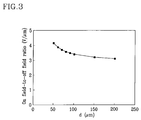
- FIG. 3 is a graph showing the relationship between an On field to Off field ratio and a distance between cathode electrodes and counter electrodes according to the present invention.
- FIG. 4 is a partial perspective view of a field emission display according to a second preferred embodiment of the present invention.
- FIG. 5 is a partial plan view of a field emission display according to a third preferred embodiment of the present invention.
- FIG. 6 is a partial plan view of a field emission display according to a fourth preferred embodiment of the present invention.
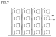
- FIG. 7 is a partial plan view of a field emission display according to a fifth preferred embodiment of the present invention.
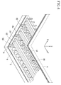
- FIG. 1 is partial perspective view of a field emission display according to a first preferred embodiment of the present invention
- FIG. 2 is a sectional view of the field emission display taken in direction A of FIG. 1.
- the FED includes a first substrate 2 of predetermined dimensions and a second substrate 4 of predetermined dimensions.
- the second substrate 4 is provided substantially in parallel to and at a certain distance apart from the first substrate 2 to form a gap between the first substrate 2 and the second substrates 4.
- the first substrate 2 will hereinafter be referred to as a rear substrate and the second substrate 4 will hereinafter be referred to as a front substrate.
- a structure that generates an electric field is provided on the rear substrate 2 and a structure that forms predetermined images by electrons emitted from the electric field is provided on the front substrate 4. This will be described in more detail below.
- a plurality of gate electrodes 6 is formed on the rear substrate 2 in a predetermined pattern.
- the gate electrodes 6 are formed in a stripe pattern along direction X of FIG. 1 at predetermined intervals.
- an insulation layer 8 is formed covering the gate electrodes 6 over an entire surface of the rear substrate 2. It is preferable that the insulation layer 8 is made of a vitreous material such as SiO 2 , polyimide, nitride, a compound of these elements, or made of a structure having these materials layered.
- a plurality of cathode electrodes 10 is formed on the insulation layer 8.
- the cathode electrodes 10 are formed in a stripe pattern along direction Y of FIG. 1 at predetermined intervals. Accordingly, the cathode electrodes 10 are perpendicular to the gate electrodes 6.
- emitters 12 are formed on the cathode electrodes.
- the emitters 12 emit electrons by generating an electric field in pixel areas of the rear substrate 2.
- each of the emitters 12 is formed covering one edge of cathode electrode and part of insulating layer. This is only one example of how the emitters 12 may be formed on the insulation, and the emitters 12 may be formed in different configurations.
- each of the emitters 12 may be formed on a center portion of the cathode electrodes 10, on one edge of the cathode electrodes 10, or both edges of the cathode electrodes 10.
- Emitters 12 are made of a carbon based material, for example, carbon nanotubes, C 60 (Fullerene), diamond, DLC (diamond-like carbon), or a combination of these materials.
- a screen-printing process a chemical vapor deposition (CVD) method, or a sputtering method may be used.
- CVD chemical vapor deposition
- sputtering method a sputtering method.
- carbon nanotubes and a screen-printing process is used.
- a plurality of counter electrodes 14 are formed on the insulation layer 8 in the pixel area.
- additional electric field is formed between the counter electrodes 14 and the emitters 12. In this manner, counter electrodes generate desirable amounts of electron emissions from the emitters.
- the counter electrodes 14 are quadrilateral and are provided in the pixel regions (as described above) between the cathode electrodes 10.
- the counter electrodes 14 may be formed in other shapes.
- the counter electrodes 14 are electrically connected to the gate electrodes 6.
- the counter electrodes are electrically connected to the gate electrodes via holes through the insulation layer.
- the connection part may be made of the same material as the counter electrodes or other conductive materials.
- the holes 8a are formed corresponding to the mounting positions of the counter electrodes 14 by a printing process or a photolithography process, etc.
- a hole can be formed by printing a layer of insulating materials in a perpendricular direction leaving an area for a hole.
- an anode electrodes R,G,B phosphor layers 18 are formed on the front substrate.
- the anode electrodes are preferably made of ITO (indium tin oxide) and patterned at a predetermined interval along direction X in Fig. 1.
- the rear substrate 2 and the front substrate 4 are provided substantially in parallel with each other and they have a predetermined gap therebetween as described above. And the cathodes are positioned perpendicular to the anode electrodes.
- the rear substrate 2 and the front substrate 4 are sealed using a sealing material 22 applied around a circumference of the rear substrate 2 and the front substrate 4, producing a single, integrally formed device.
- a plurality of spacers 20 are provided between the front substrate 2 and the rear substrate 4 in non-pixel area. The spacers 20 maintain the predetermined gap between the front substrate 2 and rear substrate 4 uniformly over the entire area.
- the FED structured as in the above, when a predetermined voltage is applied to the anode electrode 16, the cathode electrodes 10, and the gate electrodes 6, an electric field is generated between the gate electrodes 6 and the emitters 12, and electrons are emitted from the emitters 12. The emitted electrons are induced toward the phosphor layers 18 to strike the same. As a result, the phosphor layers 18 are illuminated and form predetermined images.
- reference numeral 24 indicates the additional electrical field formed between the emitters 12 and the counter electrodes 14.
- Table 1 shows variations in the magnitude of the electric field (E) with changes in the distance (d) between the cathode electrodes 10 and the counter electrodes 14. Two figures are given for each change in distance (d) - a figure for when a drive voltage is applied to the gate electrodes 6 (gate electrode On) and a figure for when a drive voltage is not applied to the gate electrodes 6 (gate electrode Off).
- FIG. 3 is a graph showing the relationship between an On field to Off field ratio (i.e., the ratio between the strength of the electric field formed on the cathode electrodes 10 when the same are On to the strength of the electric field formed on the cathode electrodes 10 when the same are Off) and the distance (d) between the cathode electrodes 10 and counter electrodes 14 referring to the calculations presented in Table 1.
- an On field to Off field ratio i.e., the ratio between the strength of the electric field formed on the cathode electrodes 10 when the same are On to the strength of the electric field formed on the cathode electrodes 10 when the same are Off
- the counter electrodes 14 have roughly the same height as that of the cathode electrodes 10.
- the first preferred embodiment of the present invention is not limited in this respect.
- FIG. 4 shows a partial perspective view of a field emission display according to a second preferred embodiment of the present invention.
- the counter electrodes are different from the first embodiment.
- same reference numerals as the first preferred embodiment are used for all elements other than the counter electrodes.
- counter electrodes 30 are mounted between the cathode electrodes 10 and are electrically connected to the gate electrodes 6 through the holes 8a of the insulation layer 8.
- the counter electrodes 30 form an electrical field between themselves and the emitters 12 and emit electrons.
- FIG. 5 shows a partial plan view of a field emission display according to a third preferred embodiment of the present invention.
- a surface of counter electrodes 32 facing emitters 34 are smoothly formed as in the above preferred embodiments. However, surfaces of the emitters 34 facing the counter electrodes 32 are formed like a saw-tooth.
- FIG. 6 shows a partial plan view of a field emission display according to a fourth preferred embodiment of the present invention.
- both the surfaces of counter electrodes 36 facing emitters 38 and surfaces of the emitters 38 facing the counter electrodes 36 are formed like a saw-tooth in the same manner.
- FIG. 7 shows a partial plan view of a field emission display according to a fifth preferred embodiment of the present invention.
- surfaces of counter electrodes 40 facing emitters 42 and surfaces of the emitters 42 facing the counter electrodes 40 are rounded. That is, the surfaces of the counter electrodes 40 facing the emitters 42 are convex-shaped, while the surfaces of the emitters 42 facing the counter electrodes 40 are concave-shaped.
- This formation of the counter electrodes 40 and the emitters 42 increases the probability of the electrons converging toward a center of the phosphor material when electrons emitted from edges of the emitters 42 are converged to phosphor material of a single pixel region (not shown). It prevents the electrons for a specific pixel region from converging onto phosphor material of an adjacent pixel region.
- the counter electrodes are provided between the cathode electrodes and connected to the gate electrodes. It forms an electric field with the emitters and supplements the electric field formed by the gate electrodes. This increases the electric field that induces the electron emission and forms the desired electric field emission with a reduced driving voltage for the gate electrodes. This also ensures that good picture quality is maintained.
Landscapes
- Chemical & Material Sciences (AREA)
- Organic Chemistry (AREA)
- Inorganic Chemistry (AREA)
- Cathode-Ray Tubes And Fluorescent Screens For Display (AREA)
- Electrodes For Cathode-Ray Tubes (AREA)
- Cold Cathode And The Manufacture (AREA)
Abstract
Description
| No. 1 | d(µm) | E1(V/µm) Gate electrode On | E2(V/µm) Gate electrode Off |
| 200 | 6.7907 | 2.1464 | |
| 2 | 150 | 6.7503 | 2.0784 |
| 3 | 100 | 6.6897 | 1.9456 |
| 4 | 90 | 6.6801 | 1.9010 |
| 5 | 80 | 6.6754 | 1.8539 |
| 6 | 70 | 6.6808 | 1.7914 |
| 7 | 60 | 6.7058 | 1.7195 |
| 8 | 50 | 6.7729 | 1.6246 |
Claims (23)
- A field emission display, comprising:wherein said first substrate are attached to said second substrate substantially parallel to each other,a first substrate;a gate electrode formed on said first substrate in a first direction;an insulating layer covering the gate electrode;a cathode electrode formed on said insulating layer in a second direction;an emitter formed on a cathode;a counter electrode formed on said insulating layer at a distance apart from said emitter and coupled to said gate electrode;a second substrate; andan anode electrode formed on said second substrate,
wherein said cathode electrode and said counter electrode face said anode electrode, and
wherein a gap is maintained evenly between said first substrate and said second substrate. - The field emission display of claim 1, wherein the first direction is perpendicular to the second direction.
- The field emission display of claim 2, wherein said counter electrode is coupled to said gate electrode via a hole through said insulating layer.
- The field emission display of claim 3, wherein said emitter is made of a carbon-based material.
- The field emission display of claim 4, wherein the distance between said cathode and said counter electrode is between 50 µm and 150 µm.
- The field emission display of claim 4, wherein said emitter and said counter electrode have similar heights.
- The field emission display of claim 4, wherein said counter electrode is higher than said emitter.
- The field emission display of claim 4, wherein an edge of said emitter facing said counter electrode is shaped like a saw-tooth.
- The field emission display of claim 8, wherein an edge of said counter electrode facing said emitter is shaped like a saw-tooth.
- The field emission display of claim 4, wherein an edge of said emitter facing said counter electrode is concave and an edge of said counter electrode facing said emitter is convex.
- The field emission display of claim 4, wherein an edge of said emitter facing said counter electrode is convex and an edge of said counter electrode facing said emitter is concave.
- The field emission display of claim 4, wherein said counter electrode is formed by electroplating.
- The field emission display of claim 4, wherein said anode electrode is a transparent conductive layer such as indium tin oxide (ITO).
- The field emission display of claim 4, wherein the carbon-based material is one of carbon nanotubes, Fullerene (C60), diamond, diamond-like carbon (DLC), or a combination of these materials.
- The field emission display of cliam 4, wherein said emitter is formed in a stripe pattern on said cathrode electrode.
- The field emission display of claim 4, wherein said emitter is formed as a separate island shape corresponding to said counter electrode.
- The field emission display of claim 4, wherein said emitter is fabricated by a screen printing method.
- The field emission display of claim 4, wherein said emitter is fabricated by a chemical vapor deposition method, or a sputtering method.
- The field emission display of claim 3, wherein the hole is formed by a photolithography method.
- The field emission display of claim 3, wherein the hole is formed by a printing method.
- The field emission display of claim 7, wherein said counter electrode is formed by a plating process.
- A method for driving a field emission display having a first substrate with a gate electrode, a cathode electrode insulated from the gate electrode, an emitter contacting the cathode electrode, a counter electrode coupled to the gate electrode and a second substrate with an anode electrode, comprising steps of:forming an electronic field between the gate electrode and the cathode electrode;enhancing the electronic field by applying a voltage to the counter electrode;emitting electrons from the emitter by forming the electronic field around the emitter.
- The method of claim 22, wherein the voltage applied to the counter electrode is the voltage applied to the gate electrode.
Applications Claiming Priority (4)
| Application Number | Priority Date | Filing Date | Title |
|---|---|---|---|
| US34433202P | 2002-01-04 | 2002-01-04 | |
| US344332P | 2002-01-04 | ||
| US10/155,732 US6621232B2 (en) | 2002-01-04 | 2002-05-28 | Field emission display device having carbon-based emitter |
| US155732 | 2002-05-28 |
Publications (3)
| Publication Number | Publication Date |
|---|---|
| EP1326264A2 true EP1326264A2 (en) | 2003-07-09 |
| EP1326264A3 EP1326264A3 (en) | 2005-02-09 |
| EP1326264B1 EP1326264B1 (en) | 2008-10-08 |
Family
ID=26852569
Family Applications (1)
| Application Number | Title | Priority Date | Filing Date |
|---|---|---|---|
| EP02019971A Expired - Lifetime EP1326264B1 (en) | 2002-01-04 | 2002-09-05 | Field emission display device |
Country Status (6)
| Country | Link |
|---|---|
| US (1) | US6621232B2 (en) |
| EP (1) | EP1326264B1 (en) |
| JP (1) | JP3995567B2 (en) |
| KR (1) | KR100852699B1 (en) |
| CN (1) | CN1288702C (en) |
| DE (1) | DE60229207D1 (en) |
Cited By (3)
| Publication number | Priority date | Publication date | Assignee | Title |
|---|---|---|---|---|
| EP1569259A1 (en) * | 2004-02-25 | 2005-08-31 | LG Electronics Inc. | Field emission display device |
| EP1571690A1 (en) * | 2004-03-05 | 2005-09-07 | Lg Electronics Inc. | Field emission display device |
| US7274137B2 (en) | 2003-11-24 | 2007-09-25 | Samsung Sdi Co., Ltd | Electron emission device with emission controlling resistance layer |
Families Citing this family (36)
| Publication number | Priority date | Publication date | Assignee | Title |
|---|---|---|---|---|
| CN100407362C (en) * | 2002-04-12 | 2008-07-30 | 三星Sdi株式会社 | field emission display |
| KR100459904B1 (en) * | 2002-08-05 | 2004-12-03 | 삼성에스디아이 주식회사 | Field emission display with separated upper electrode structure |
| KR100879292B1 (en) * | 2002-12-20 | 2009-01-19 | 삼성에스디아이 주식회사 | Field emission display with emitter array structure to improve electron emission characteristics |
| KR100893685B1 (en) * | 2003-02-14 | 2009-04-17 | 삼성에스디아이 주식회사 | Field emission indicator with grid plate |
| JP2004259577A (en) * | 2003-02-26 | 2004-09-16 | Hitachi Displays Ltd | Flat-plate type image display device |
| KR100932975B1 (en) * | 2003-03-27 | 2009-12-21 | 삼성에스디아이 주식회사 | Field emission display device with multi-layered grid plate |
| KR20050014430A (en) * | 2003-07-31 | 2005-02-07 | 삼성에스디아이 주식회사 | A composition for forming a electron emitter of flat panel display and electron emitter prepared therefrom |
| KR100523840B1 (en) | 2003-08-27 | 2005-10-27 | 한국전자통신연구원 | Field Emission Device |
| KR20050041726A (en) * | 2003-10-31 | 2005-05-04 | 삼성에스디아이 주식회사 | Field emission display device and manufacturing method of the same |
| KR100556745B1 (en) * | 2003-11-04 | 2006-03-10 | 엘지전자 주식회사 | Field emission devices |
| KR100965543B1 (en) * | 2003-11-29 | 2010-06-23 | 삼성에스디아이 주식회사 | Field emission display device and manufacturing method thereof |
| KR20050060748A (en) * | 2003-12-17 | 2005-06-22 | 삼성에스디아이 주식회사 | Field emission display using carbon nanotube and manufacturing method thereof |
| KR101018344B1 (en) * | 2004-01-08 | 2011-03-04 | 삼성에스디아이 주식회사 | Field emission backlight unit, its driving method and manufacturing method of lower panel |
| KR20050078327A (en) * | 2004-01-29 | 2005-08-05 | 삼성에스디아이 주식회사 | Field emission display device and manufacturing method of the same |
| JP2005235748A (en) * | 2004-02-17 | 2005-09-02 | Lg Electronics Inc | Carbon nanotube field emission element and driving method thereof |
| KR100982329B1 (en) * | 2004-02-20 | 2010-09-15 | 삼성에스디아이 주식회사 | Field emission display device and manufacturing method thereof |
| KR100982328B1 (en) * | 2004-02-25 | 2010-09-15 | 삼성에스디아이 주식회사 | Field emission display |
| ATE360882T1 (en) * | 2004-02-26 | 2007-05-15 | Samsung Sdi Co Ltd | ELECTRON EMISSION DEVICE |
| KR20040031756A (en) * | 2004-03-25 | 2004-04-13 | 우형수 | Field emission display device and method for manufacturing the device |
| KR20050096536A (en) * | 2004-03-31 | 2005-10-06 | 삼성에스디아이 주식회사 | Electron emission display with grid electrode |
| KR20050096532A (en) * | 2004-03-31 | 2005-10-06 | 삼성에스디아이 주식회사 | Electron emission device and electron emission display using the same |
| KR20050111706A (en) * | 2004-05-22 | 2005-11-28 | 삼성에스디아이 주식회사 | Field emission display and method for manufacturing the same |
| KR20050113863A (en) * | 2004-05-31 | 2005-12-05 | 삼성에스디아이 주식회사 | Electron emission device |
| KR20060020017A (en) * | 2004-08-30 | 2006-03-06 | 삼성에스디아이 주식회사 | Electron emitting device and method for manufacturing same |
| KR20060019845A (en) * | 2004-08-30 | 2006-03-06 | 삼성에스디아이 주식회사 | Electron-emitting device |
| KR20060095320A (en) * | 2005-02-28 | 2006-08-31 | 삼성에스디아이 주식회사 | Electron-emitting device |
| KR20060095331A (en) * | 2005-02-28 | 2006-08-31 | 삼성에스디아이 주식회사 | Electron-emitting device |
| KR20060104652A (en) * | 2005-03-31 | 2006-10-09 | 삼성에스디아이 주식회사 | Electron-emitting device |
| KR20060104657A (en) | 2005-03-31 | 2006-10-09 | 삼성에스디아이 주식회사 | Electron-emitting device |
| KR20060124332A (en) * | 2005-05-31 | 2006-12-05 | 삼성에스디아이 주식회사 | Electron-emitting device |
| CN100573063C (en) * | 2005-06-15 | 2009-12-23 | 中国科学院上海微系统与信息技术研究所 | Micro mechanical Nano tube field emission type non-refrigerant thermal imaging device and method for making |
| KR20070001377A (en) * | 2005-06-29 | 2007-01-04 | 삼성에스디아이 주식회사 | Electron emitting device and driving method thereof |
| CN100365755C (en) * | 2005-10-18 | 2008-01-30 | 中原工学院 | Planar light-emitting display with lower gate structure and its manufacturing process |
| CN100367443C (en) * | 2005-10-18 | 2008-02-06 | 中原工学院 | Transistor structure reflective light-emitting flat panel display and its manufacturing process |
| KR20070103909A (en) * | 2006-04-20 | 2007-10-25 | 삼성에스디아이 주식회사 | Electron emission indicator |
| KR20070111689A (en) * | 2006-05-18 | 2007-11-22 | 삼성에스디아이 주식회사 | Electron Emission Device and Electron Emission Display Device Using The Same |
Family Cites Families (6)
| Publication number | Priority date | Publication date | Assignee | Title |
|---|---|---|---|---|
| KR100312694B1 (en) * | 1999-07-16 | 2001-11-03 | 김순택 | Fed having a carbon nanotube film as emitters |
| JP2001035352A (en) * | 1999-07-22 | 2001-02-09 | Sharp Corp | Electron source, method of manufacturing the same, and image forming apparatus formed using the same |
| JP4298156B2 (en) * | 1999-12-08 | 2009-07-15 | キヤノン株式会社 | Electron emission apparatus and image forming apparatus |
| KR100477739B1 (en) * | 1999-12-30 | 2005-03-18 | 삼성에스디아이 주식회사 | Field emission device and driving method thereof |
| GB0006762D0 (en) * | 2000-03-22 | 2000-05-10 | Smiths Industries Plc | Displays |
| KR100749460B1 (en) * | 2001-04-25 | 2007-08-14 | 삼성에스디아이 주식회사 | Field emission display device and manufacturing method thereof |
-
2002
- 2002-05-28 US US10/155,732 patent/US6621232B2/en not_active Expired - Fee Related
- 2002-06-12 KR KR1020020032904A patent/KR100852699B1/en not_active Expired - Fee Related
- 2002-09-05 DE DE60229207T patent/DE60229207D1/en not_active Expired - Lifetime
- 2002-09-05 EP EP02019971A patent/EP1326264B1/en not_active Expired - Lifetime
- 2002-09-13 JP JP2002267584A patent/JP3995567B2/en not_active Expired - Fee Related
- 2002-09-16 CN CNB021431906A patent/CN1288702C/en not_active Expired - Fee Related
Cited By (3)
| Publication number | Priority date | Publication date | Assignee | Title |
|---|---|---|---|---|
| US7274137B2 (en) | 2003-11-24 | 2007-09-25 | Samsung Sdi Co., Ltd | Electron emission device with emission controlling resistance layer |
| EP1569259A1 (en) * | 2004-02-25 | 2005-08-31 | LG Electronics Inc. | Field emission display device |
| EP1571690A1 (en) * | 2004-03-05 | 2005-09-07 | Lg Electronics Inc. | Field emission display device |
Also Published As
| Publication number | Publication date |
|---|---|
| CN1430241A (en) | 2003-07-16 |
| KR100852699B1 (en) | 2008-08-19 |
| US20030127988A1 (en) | 2003-07-10 |
| US6621232B2 (en) | 2003-09-16 |
| EP1326264B1 (en) | 2008-10-08 |
| JP3995567B2 (en) | 2007-10-24 |
| EP1326264A3 (en) | 2005-02-09 |
| DE60229207D1 (en) | 2008-11-20 |
| JP2003217485A (en) | 2003-07-31 |
| KR20030060045A (en) | 2003-07-12 |
| CN1288702C (en) | 2006-12-06 |
Similar Documents
| Publication | Publication Date | Title |
|---|---|---|
| US6621232B2 (en) | Field emission display device having carbon-based emitter | |
| KR20050086238A (en) | Field emission display device | |
| US6750604B2 (en) | Field emission display panels incorporating cathodes having narrow nanotube emitters formed on dielectric layers | |
| US6486599B2 (en) | Field emission display panel equipped with two cathodes and an anode | |
| KR101009983B1 (en) | Electron emission display device | |
| US7173365B2 (en) | Field emission display having emitter arrangement structure capable of enhancing electron emission characteristics | |
| US7301268B2 (en) | Field emission display having emitter arrangement structure capable of enhancing electron emission characteristics | |
| US7612493B2 (en) | Electron emission device with improved focusing of electron beams | |
| US20040155572A1 (en) | Field emission display having carbon-based emitters | |
| US7432645B2 (en) | Electron emission device and electron emission display using the same | |
| US20030071257A1 (en) | Field emission display having improved capability of converging electron beams | |
| KR20060104659A (en) | Electron-emitting device | |
| KR20060104655A (en) | Electron-emitting device | |
| US20060113889A1 (en) | Electron emission device | |
| KR100357348B1 (en) | A field emission display and manufacturing method for it | |
| US7728496B2 (en) | Electron emission device having curved surface electron emission region | |
| KR100903615B1 (en) | Spacer for Electron Emission Display and Electron Emission Display | |
| JP2006066376A (en) | Electron emitter | |
| KR100884528B1 (en) | Field emission indicator | |
| US20060113888A1 (en) | Field emission display device with protection structure | |
| KR20060060482A (en) | Electron emitting device and manufacturing method thereof | |
| KR20070044175A (en) | Electron emitting device and electron emitting device having same | |
| KR20050005270A (en) | Field emission display device and its manufacturing method | |
| KR20070041990A (en) | Electron emitting device and electron emitting device having same | |
| KR20040021396A (en) | Field emission display device having self focusing electrode |
Legal Events
| Date | Code | Title | Description |
|---|---|---|---|
| PUAI | Public reference made under article 153(3) epc to a published international application that has entered the european phase |
Free format text: ORIGINAL CODE: 0009012 |
|
| AK | Designated contracting states |
Designated state(s): AT BE BG CH CY CZ DE DK EE ES FI FR GB GR IE IT LI LU MC NL PT SE SK TR |
|
| AX | Request for extension of the european patent |
Extension state: AL LT LV MK RO SI |
|
| PUAL | Search report despatched |
Free format text: ORIGINAL CODE: 0009013 |
|
| AK | Designated contracting states |
Kind code of ref document: A3 Designated state(s): AT BE BG CH CY CZ DE DK EE ES FI FR GB GR IE IT LI LU MC NL PT SE SK TR |
|
| AX | Request for extension of the european patent |
Extension state: AL LT LV MK RO SI |
|
| 17P | Request for examination filed |
Effective date: 20050718 |
|
| AKX | Designation fees paid |
Designated state(s): DE FR GB |
|
| 17Q | First examination report despatched |
Effective date: 20060207 |
|
| RTI1 | Title (correction) |
Free format text: FIELD EMISSION DISPLAY DEVICE |
|
| GRAP | Despatch of communication of intention to grant a patent |
Free format text: ORIGINAL CODE: EPIDOSNIGR1 |
|
| RAP1 | Party data changed (applicant data changed or rights of an application transferred) |
Owner name: SAMSUNG SDI CO. LTD. |
|
| RAP1 | Party data changed (applicant data changed or rights of an application transferred) |
Owner name: SAMSUNG SDI CO. LTD. |
|
| GRAS | Grant fee paid |
Free format text: ORIGINAL CODE: EPIDOSNIGR3 |
|
| GRAA | (expected) grant |
Free format text: ORIGINAL CODE: 0009210 |
|
| AK | Designated contracting states |
Kind code of ref document: B1 Designated state(s): DE FR GB |
|
| REG | Reference to a national code |
Ref country code: GB Ref legal event code: FG4D |
|
| REF | Corresponds to: |
Ref document number: 60229207 Country of ref document: DE Date of ref document: 20081120 Kind code of ref document: P |
|
| PLBE | No opposition filed within time limit |
Free format text: ORIGINAL CODE: 0009261 |
|
| STAA | Information on the status of an ep patent application or granted ep patent |
Free format text: STATUS: NO OPPOSITION FILED WITHIN TIME LIMIT |
|
| 26N | No opposition filed |
Effective date: 20090709 |
|
| PGFP | Annual fee paid to national office [announced via postgrant information from national office to epo] |
Ref country code: FR Payment date: 20110725 Year of fee payment: 10 |
|
| PGFP | Annual fee paid to national office [announced via postgrant information from national office to epo] |
Ref country code: DE Payment date: 20110629 Year of fee payment: 10 Ref country code: GB Payment date: 20110802 Year of fee payment: 10 |
|
| GBPC | Gb: european patent ceased through non-payment of renewal fee |
Effective date: 20120905 |
|
| REG | Reference to a national code |
Ref country code: FR Ref legal event code: ST Effective date: 20130531 |
|
| PG25 | Lapsed in a contracting state [announced via postgrant information from national office to epo] |
Ref country code: GB Free format text: LAPSE BECAUSE OF NON-PAYMENT OF DUE FEES Effective date: 20120905 Ref country code: DE Free format text: LAPSE BECAUSE OF NON-PAYMENT OF DUE FEES Effective date: 20130403 |
|
| PG25 | Lapsed in a contracting state [announced via postgrant information from national office to epo] |
Ref country code: FR Free format text: LAPSE BECAUSE OF NON-PAYMENT OF DUE FEES Effective date: 20121001 |
|
| REG | Reference to a national code |
Ref country code: DE Ref legal event code: R119 Ref document number: 60229207 Country of ref document: DE Effective date: 20130403 |