EP1326250A2 - Voltage detection circuit control device, memory control device wth the same, and memory card with the same - Google Patents
Voltage detection circuit control device, memory control device wth the same, and memory card with the same Download PDFInfo
- Publication number
- EP1326250A2 EP1326250A2 EP02028778A EP02028778A EP1326250A2 EP 1326250 A2 EP1326250 A2 EP 1326250A2 EP 02028778 A EP02028778 A EP 02028778A EP 02028778 A EP02028778 A EP 02028778A EP 1326250 A2 EP1326250 A2 EP 1326250A2
- Authority
- EP
- European Patent Office
- Prior art keywords
- voltage detection
- circuit
- detection circuit
- signal
- voltage
- Prior art date
- Legal status (The legal status is an assumption and is not a legal conclusion. Google has not performed a legal analysis and makes no representation as to the accuracy of the status listed.)
- Withdrawn
Links
Images


Classifications
-
- G—PHYSICS
- G11—INFORMATION STORAGE
- G11C—STATIC STORES
- G11C5/00—Details of stores covered by group G11C11/00
- G11C5/14—Power supply arrangements, e.g. power down, chip selection or deselection, layout of wirings or power grids, or multiple supply levels
- G11C5/143—Detection of memory cassette insertion or removal; Continuity checks of supply or ground lines; Detection of supply variations, interruptions or levels ; Switching between alternative supplies
Definitions
- the present invention relates to a control for disabling and restoring the operation of a voltage detection circuit.
- SD (Secure Disk) cards have widely been used more and more as external storage devices that are small in size and excellent in portability and information security.
- the operational power supply is defined in two stages.
- two kinds of power supply voltage detection circuits need to be provided. Normally, since two voltage detection circuits are always activated, operation power is always consumed by the two circuits.
- Jpn. Pat. Appln. KOKAI Publication No. 5-74136 discloses a technique for increasing the life of a cell for a memory card, in order to reduce power consumption of the memory card.
- cell voltage detection in the memory card is performed only in a short time period in which external power is supplied to the memory card.
- a cell is connected to a switch-operable element, and an output of this element is delivered to a cell voltage detection element.
- An output of the cell voltage detection element is supplied to a latch circuit, and an output of the latch circuit is delivered to a connector of the memory card.
- a voltage detection circuit control device comprises: a first voltage detection circuit which detects a first voltage; a second voltage detection circuit which detects a second voltage higher than the first voltage; and an operation signal generating circuit which is connected to the first and second voltage detection circuits and produces a signal for controlling an operation of the first voltage detection circuit on the basis of a voltage detection signal from the second voltage detection circuit.
- a memory control device comprises: a host interface circuit; a back-end circuit; a first voltage detection circuit which detects a first voltage and produces a drive signal for the host interface circuit; a second voltage detection circuit which detects a second voltage higher than the first voltage and produces a drive signal for the back-end circuit; and an operation signal generating circuit which is connected to the first and second voltage detection circuits and produces a signal for controlling an operation of the first voltage detection circuit on the basis of the back-end circuit drive signal from the second voltage detection circuit.
- a voltage detection circuit control device according to the present invention as well as an SD card that is a non-volatile memory card, to which a memory control device having the voltage detection circuit control device is applied.
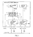
- FIG. 1 is a block diagram showing a circuit configuration including a voltage detection circuit arranged within a non-volatile memory controller provided in an SD card.
- a host interface circuit 1 controls transmission/reception of signals with a host device to be connected.
- circuit groups 2 which are referred to as "back-end circuit", are controlled by a microcomputer that is provided in the SD card to control internal operations.
- Numeral 3 denotes a 1.6V voltage detection circuit that has an enable terminal ( res ) and detects the presence/absence of supply of 1.6V power from a power line.
- Numeral 4 denotes a 2.7V voltage detection circuit that has an enable terminal ( res ) and detects the presence/absence of supply of 2.7V power from the power line.
- Numeral 5 designates a selection signal for activating or inactivating a low-power-consumption mode that automatically disables (halts) a low-voltage-side voltage detection circuit, i.e. the 1.6V voltage detection circuit, by an operation according to the present embodiment, as described below.
- Numerals 6 and 8 denote power input signal lines to which 1.6V and 3.6V are applied from the power supply voltage line.
- Numerals 6 and 9 denote ground signal lines (GND).
- Numeral 11 denotes an operation signal generating circuit for the 1.6V voltage detection circuit, which generates a disable signal 16 for disabling or enabling the operation of the 1.6V voltage detection circuit 3.
- the operation signal generating circuit 11 for the 1.6V voltage detection circuit includes a selector for selecting a mode for supplying a detection signal from the 1.6V voltage detection circuit 3 to a reset signal 18 for the host interface circuit 1, or a mode for producing a logic output of the operation signal generating circuit 11 for the 1.6V voltage detection circuit.
- a signal line 17 extends from the 2.7V voltage detection circuit 4. Specifically, the signal line 17 is a reset signal (-BE_RES) connected to the back-end circuit 2.
- FIG. 2 is a circuit block diagram of the operation signal generating circuit 11 for the 1.6V voltage detection circuit.
- a line 13 is supplied with an output signal (reset signal) from the 2.7V voltage detection circuit 4, and a line 14 is supplied with an output signal from the 1.6V voltage detection circuit 3.
- a reset signal line (-HIM_RES) 18 functions to reset the host interface circuit 1 when the operation mode of the present embodiment has been rendered effective.
- a signal line 16 supplies a control signal for disabling or enabling the operation of the 1.6V voltage detection circuit 3.
- a delay element 19 delays the output signal (reset signal) 13 from the 2.7V voltage detection circuit 4.
- Numeral 20 denotes an OR circuit, and numeral 21 denotes an AND circuit.
- Numeral 22 denotes a delay signal line that delivers a signal obtained by delaying the output signal (reset signal) 13 from the 2.7V voltage detection circuit 4 by a delay element 19.
- a control sequence of the 1.6V voltage detection circuit 3 according to the present embodiment as described with reference to FIGS. 1 and 2 will now be described with reference to a control sequence chart of FIG. 3 and a flow chart of FIG. 4.
- the 1.6V voltage detection circuit 3 detects a 1.6V voltage and sets an output to the output signal line 14 of the 1.6V voltage detection circuit at "H" level (i.e. release of reset). Thereby, the circuit component connected to the -HIM_RES signal line 18, which is in turn connected to the host interface circuit 1, begins to operate.
- the 2.7V voltage detection circuit 4 detects a 2.7V voltage and switches an output to the 2.7V voltage detection circuit output signal line 17 from "L” to "H” (release of reset). At this time point, the circuit connected to the -BE_RES signal line 17, which is in turn connected to the back-end circuit 2, begins to operate.
- a DV_CTL signal line 5 is fixed at "H" on the outside of the chip.
- the AND circuit 21 shown in FIG. 2 passes the output signal 13 from the 2.7V voltage detection circuit 4 to the line 16, thus setting the reset input ( res input) of the 1.6V voltage detection circuit 3 at "H". Thereby, power-down of the 1.6V voltage detection circuit 3 is effected, and the power consumed up to now is saved.
- the 1.6V out signal (detection signal) 14 from the 1.6V voltage detection circuit 3 is made effective by the OR circuit 20 within the operation signal generating circuit 11 for the 1.6V voltage detection circuit, until the 1.6V voltage detection circuit 3 powers down. While the 1.6V voltage detection circuit 3 powers down, the 2.7V out signal (detection signal) 13 from the 2.7V voltage detection circuit 4 is made effective. After the 2.7V out signal (detection signal) 13 from the 2.7V voltage detection circuit 4 has reached "H" level, the 1.6V voltage detection circuit 3 powers down. Thus, a chattering noise does not occur by the OR operation for the 2.7V out signal and 1.6V out signal.
- the 2.7V voltage detection circuit 4 changes its output signal (detection signal) 13 from “H” to "L". Then, the 1.6V voltage detection circuit 3 enters the restoration operation. However, since some delay occurs until the restoration, the signal 22 obtained by delaying the 2.7V out signal (output signal) 13 from the 2.7V voltage detection circuit 4 by the delay element 19 is subjected to the OR operation in the OR circuit 20. Accordingly, no chattering noise occurs, and the -HIM_RES signal (reset signal) 18 to the host interface circuit 1 can be produced.
- the -HIM_RES signal 18 to the host interface circuit 1 can be produced by 2.7 out + 1.6 out + DLY_ 2.7 (in this context, sign "+” indicates a logic operation "OR”).
- FIG. 4 is a flow chart illustrating the power-down operation of the 1.6V voltage detection circuit 3.
- the voltage supplied from the power supply line rises (step S1).
- the 1.6V voltage detection circuit 3 detects whether the supply voltage from the power supply line has reached 1.6V (step S2). This operation is repeated until the supply voltage reaches 1.6V (NO in step S2). If it is detected that the supply voltage has reached 1.6V (YES in step S4), resetting of the host interface circuit 1 on the 1.6V side is released (step S3).
- the supply voltage is continuously monitored.
- the 2.7V voltage detection circuit 4 detects whether the supply voltage from the power supply line has reached 2.7V (step S4). This operation is repeated until the supply voltage reaches 2.7V (NO in step S4). If it is detected that the supply voltage has reached 2.7V (YES in step S4), resetting of the back-end circuit 2 on the 2.7V side is released (step S5).
- the operation signal generating circuit 11 for the 1.6V voltage detection circuit receives the output signal 13 from the 2.7V voltage detection circuit 4, and the reset signal 16 resets the 1.6V voltage detection circuit 3 (step S6).
- the system is in operation (step S7) and the power consumed by the 1.6V voltage detection circuit 3 can be saved.
- step S8 the voltage supplied from the power supply line decreases.
- step S9 The 2.7V voltage detection circuit 4 detects whether the supply voltage from the power supply line has reached 2.7V (step S9). This operation is repeated until the supply voltage reaches 2.7V (NO in step S9). If it is detected that the supply voltage has reached 2.7V (YES in step S9), resetting of the back-end circuit 2 on the 2.7V side is executed (step S10).
- the operation signal generating circuit 11 for the 1.6V voltage detection circuit receives the output signal 13 from the 2.7V voltage detection circuit 4, and the restoration signal 16 releases the reset state of the 1.6V voltage detection circuit 3.
- the 1.6V voltage detection circuit 3 is set in the restored state.
- release of the power-down state of the 1.6V voltage detection circuit 3 is executed (step S11).
- step S12 The supply voltage is continuously monitored, and 1.6V voltage detection circuit 3 detects whether the supply voltage from the power supply line has reached 1.6V (step S12). This operation is repeated until the supply voltage reaches 1.6V (NO in step S12). If it is detected that the supply voltage has reached 1.6V (YES in step S12), resetting of the host interface circuit 1 on the 1.6V side is executed (step S13). In this state, the operation of the system is finished, and the power-off is completed (step S14).
- FIG. 6 shows a simplified structure of the structure shown in FIG. 2, which includes a plurality of voltage detection circuits and a plurality of operation signal generating circuits for the voltage detection circuits.
- this modification is the same as that of the above-described embodiment. In this modification, three voltages are detected. Even if four or more voltage detection circuits are connected, the operation will remain the same.
- the voltage detection is effected in the following order: voltage detection circuit C (HIGH_V: high voltage detection) 55 ⁇ voltage detection circuit B (MID_V: middle voltage detection) 45 ⁇ voltage detection circuit A (LOW_V: low voltage detection) 35.
- Reset signals are set in the LOW state in succession in the following order: signal line 54 ⁇ signal line 44 ⁇ signal line 34.
- the timing of disabling the voltage detection circuit that is one rank below is the same as the timing shown in FIG. 3 according to the above-described embodiment.
- the output signal 43 of operation signal generating circuit 42 of voltage detection circuit B enables (power-down/restoration) the voltage detection circuit B (MID_V: middle voltage detection) 45.
- the output signal 33 of operation signal generating circuit 32 of voltage detection circuit A enables the voltage detection circuit A (LOW_V: low voltage detection) 35.
- the voltage detection circuits i.e. voltage detection circuit B (MID_V: middle voltage detection) 45 and voltage detection circuit A (LOW_V: low voltage detection) 35
- the voltage detection circuit C HIGH_V: high voltage detection
- the voltage detection circuits can be powered down to the normal operation state, i.e. a higher voltage state than the detection voltage of the voltage detection circuit C (HIGH_V: high voltage detection) 55.
Landscapes
- Engineering & Computer Science (AREA)
- Power Engineering (AREA)
- Power Sources (AREA)
- Measurement Of Current Or Voltage (AREA)
- Techniques For Improving Reliability Of Storages (AREA)
- Credit Cards Or The Like (AREA)
Abstract
Description
Claims (9)
- A voltage detection circuit control device characterized by comprising:a first voltage detection circuit (3) which detects a first voltage;a second voltage detection circuit (4) which detects a second voltage higher than the first voltage; andan operation signal generating circuit (11) which is connected to the first and second voltage detection circuits and produces a signal for controlling an operation of the first voltage detection circuit on the basis of a voltage detection signal from the second voltage detection circuit.
- A voltage detection circuit control device according to claim 1, characterized in that the operation signal generating circuit transmits an operation control signal to the first voltage detection circuit, and the operation control signal is a signal for disabling the operation of the first voltage detection circuit.
- A voltage detection circuit control device according to claim 1, characterized in that the operation signal generating circuit transmits an operation control signal to the first voltage detection circuit, and the operation control signal is a signal for restoring the operation of the first voltage detection circuit.
- A voltage detection circuit control device according to claim 1, characterized in that the operation signal generating circuit comprises:a delay circuit which delays the detection signal from the second voltage detection circuit; andan OR circuit which produces a signal corresponding to the detection signal of the first voltage detection circuit, on the basis of an output signal of the delay circuit and the detection signal from the second voltage detection circuit.
- A memory control device characterized by comprising:a host interface circuit (1);a back-end circuit (2);a first voltage detection circuit (3) which detects a first voltage and produces a drive signal for the host interface circuit;a second voltage detection circuit (4) which detects a second voltage higher than the first voltage and produces a drive signal for the back-end circuit; andan operation signal generating circuit (11) which is connected to the first and second voltage detection circuits and produces a signal for controlling an operation of the first voltage detection circuit on the basis of the back-end circuit drive signal from the second voltage detection circuit.
- A memory control device according to claim 5, characterized in that the operation signal generating circuit transmits an operation control signal to the first voltage detection circuit, and the operation control signal is a signal for disabling the operation of the first voltage detection circuit.
- A memory control device according to claim 5, characterized in that the operation signal generating circuit transmits an operation control signal to the first voltage detection circuit, and the operation control signal is a signal for restoring the operation of the first voltage detection circuit.
- A memory control device according to claim 5, characterized in that the operation signal generating circuit comprises:a delay circuit which delays the operation signal for the back-end circuit from the second voltage detection circuit; andan OR circuit which produces an operation signal for the host interface circuit, on the basis of an output signal of the delay circuit and the back-end circuit operation signal from the second voltage detection circuit.
- A memory card characterized by comprising:a host interface circuit (1);a back-end circuit (2);a first voltage detection circuit (3) which detects a first voltage and produces a drive signal for the host interface circuit;a second voltage detection circuit (4) which detects a second voltage higher than the first voltage and produces a drive signal for the back-end circuit; andan operation signal generating circuit (11) which is connected to the first and second voltage detection circuits and produces a signal for controlling an operation of the first voltage detection circuit on the basis of the back-end circuit drive signal from the second voltage detection circuit.
Applications Claiming Priority (2)
| Application Number | Priority Date | Filing Date | Title |
|---|---|---|---|
| JP2001395682 | 2001-12-27 | ||
| JP2001395682A JP3933467B2 (en) | 2001-12-27 | 2001-12-27 | Voltage detection circuit control device, memory control device having the same device, and memory card having the same device |
Publications (2)
| Publication Number | Publication Date |
|---|---|
| EP1326250A2 true EP1326250A2 (en) | 2003-07-09 |
| EP1326250A3 EP1326250A3 (en) | 2004-01-21 |
Family
ID=19189017
Family Applications (1)
| Application Number | Title | Priority Date | Filing Date |
|---|---|---|---|
| EP02028778A Withdrawn EP1326250A3 (en) | 2001-12-27 | 2002-12-23 | Voltage detection circuit control device, memory control device wth the same, and memory card with the same |
Country Status (4)
| Country | Link |
|---|---|
| US (2) | US7196944B2 (en) |
| EP (1) | EP1326250A3 (en) |
| JP (1) | JP3933467B2 (en) |
| CN (1) | CN100409369C (en) |
Families Citing this family (10)
| Publication number | Priority date | Publication date | Assignee | Title |
|---|---|---|---|---|
| US7212067B2 (en) * | 2003-08-01 | 2007-05-01 | Sandisk Corporation | Voltage regulator with bypass for multi-voltage storage system |
| US7164561B2 (en) * | 2004-02-13 | 2007-01-16 | Sandisk Corporation | Voltage regulator using protected low voltage devices |
| US7391193B2 (en) * | 2005-01-25 | 2008-06-24 | Sandisk Corporation | Voltage regulator with bypass mode |
| JP2012234591A (en) * | 2011-04-28 | 2012-11-29 | Toshiba Corp | Nonvolatile semiconductor storage device |
| KR101939701B1 (en) * | 2012-02-14 | 2019-01-18 | 삼성전자주식회사 | Power supply circuit, power supply method |
| JP6441619B2 (en) * | 2014-09-03 | 2018-12-19 | ルネサスエレクトロニクス株式会社 | Semiconductor device |
| US9747958B2 (en) * | 2015-10-30 | 2017-08-29 | Sandisk Technologies Llc | Device soft-start management for enumeration problems with USB hosts |
| CN107886981B (en) * | 2017-11-28 | 2021-04-27 | 晶晨半导体(上海)股份有限公司 | A power-down processing method applied to embedded system |
| JP6792667B2 (en) * | 2019-05-13 | 2020-11-25 | ウィンボンド エレクトロニクス コーポレーション | Semiconductor storage device |
| JP6748760B1 (en) * | 2019-05-13 | 2020-09-02 | ウィンボンド エレクトロニクス コーポレーション | Semiconductor memory device |
Family Cites Families (14)
| Publication number | Priority date | Publication date | Assignee | Title |
|---|---|---|---|---|
| JPS6318074A (en) * | 1986-07-11 | 1988-01-25 | Teijin Ltd | Thin film forming device |
| JP2842588B2 (en) * | 1987-01-26 | 1999-01-06 | 日本電気株式会社 | Voltage detection circuit |
| US5051995A (en) * | 1988-03-14 | 1991-09-24 | Mitsubishi Denki Kabushiki Kaisha | Semiconductor memory device having a test mode setting circuit |
| JPH04157372A (en) | 1990-10-19 | 1992-05-29 | Nec Corp | Window type voltage comparator circuit |
| JPH0574136A (en) | 1991-09-12 | 1993-03-26 | Seiko Epson Corp | memory card |
| JPH05137253A (en) * | 1991-11-11 | 1993-06-01 | Mitsubishi Electric Corp | Abnormal voltage detection controller |
| JPH05143802A (en) * | 1991-11-15 | 1993-06-11 | Seiko Epson Corp | memory card |
| JP2590725B2 (en) | 1994-03-09 | 1997-03-12 | カシオ計算機株式会社 | Music data input device |
| CN1109347C (en) * | 1994-10-19 | 2003-05-21 | 英特尔公司 | Flash memory power |
| JP4299883B2 (en) * | 1995-11-13 | 2009-07-22 | レクサー・メディア・インコーポレーテッド | Automatic voltage detection when multiple voltages are applied |
| US5822246A (en) * | 1996-09-30 | 1998-10-13 | Intel Corporation | Method and apparatus for detecting the voltage on the VCC pin |
| US5943263A (en) * | 1997-01-08 | 1999-08-24 | Micron Technology, Inc. | Apparatus and method for programming voltage protection in a non-volatile memory system |
| JP3230502B2 (en) | 1998-11-20 | 2001-11-19 | 日本電気株式会社 | Voltage detection circuit |
| JP2004297028A (en) * | 2003-02-04 | 2004-10-21 | Sharp Corp | Semiconductor memory device |
-
2001
- 2001-12-27 JP JP2001395682A patent/JP3933467B2/en not_active Expired - Fee Related
-
2002
- 2002-12-23 US US10/325,755 patent/US7196944B2/en not_active Expired - Fee Related
- 2002-12-23 EP EP02028778A patent/EP1326250A3/en not_active Withdrawn
- 2002-12-27 CN CNB021608784A patent/CN100409369C/en not_active Expired - Fee Related
-
2006
- 2006-07-07 US US11/481,819 patent/US7203104B2/en not_active Expired - Fee Related
Also Published As
| Publication number | Publication date |
|---|---|
| US7203104B2 (en) | 2007-04-10 |
| US20030132733A1 (en) | 2003-07-17 |
| CN100409369C (en) | 2008-08-06 |
| EP1326250A3 (en) | 2004-01-21 |
| JP3933467B2 (en) | 2007-06-20 |
| US7196944B2 (en) | 2007-03-27 |
| JP2003196623A (en) | 2003-07-11 |
| US20060250875A1 (en) | 2006-11-09 |
| CN1430228A (en) | 2003-07-16 |
Similar Documents
| Publication | Publication Date | Title |
|---|---|---|
| US6348744B1 (en) | Integrated power management module | |
| US7161834B2 (en) | Memory card and data processing system | |
| US8032259B2 (en) | Bi-directional power control | |
| EP0861468B1 (en) | Automatic voltage detection in multiple voltage applications | |
| US6727952B1 (en) | Electronic device having common connector | |
| JP2003091703A (en) | Card device | |
| US20020181311A1 (en) | Semiconductor memory unit in which power consumption can be restricted | |
| US7203104B2 (en) | Voltage detection circuit control device, memory control device with the same, and memory card with the same | |
| KR20210007050A (en) | Host apparatus and extension device | |
| KR100343028B1 (en) | Power supply detection scheme for flash memory | |
| US20090077393A1 (en) | Card-type electronic device and host device | |
| US20040210779A1 (en) | Control circuit for power voltage | |
| US7378896B2 (en) | Single pin for multiple functional control purposes | |
| CN101207378B (en) | Bidirectional signal interface and related system and method | |
| US6996727B1 (en) | Power supply for universal serial bus interface with programmable bus pullup resistor | |
| US9331673B2 (en) | Integrated circuit operating active circuitry and chip pads in different operating modes and at different voltage levels | |
| US6653880B2 (en) | Semiconductor integrated circuit device forming power sources having different voltages for operating circuit blocks | |
| CN101202458B (en) | Power supply circuit | |
| US20240393854A1 (en) | Host device, slave device, and host-slave system | |
| US12620804B2 (en) | Power management in a near field communication controller | |
| US12254916B2 (en) | Memory device | |
| CN217388206U (en) | Power-on time sequence control circuit based on online power supply burning | |
| KR100686933B1 (en) | Power Stabilization Circuit of Semiconductor Device | |
| US7512823B2 (en) | Semiconductor device with reduced power consumption that selectively drives one of a plurality of signal receivers according to level of external supply voltage | |
| WO2009005506A1 (en) | Systems and methods for implementing standby functionality using field programmable gate arrays |
Legal Events
| Date | Code | Title | Description |
|---|---|---|---|
| PUAI | Public reference made under article 153(3) epc to a published international application that has entered the european phase |
Free format text: ORIGINAL CODE: 0009012 |
|
| 17P | Request for examination filed |
Effective date: 20021223 |
|
| AK | Designated contracting states |
Designated state(s): AT BE BG CH CY CZ DE DK EE ES FI FR GB GR IE IT LI LU MC NL PT SE SI SK TR |
|
| AX | Request for extension of the european patent |
Extension state: AL LT LV MK RO |
|
| PUAL | Search report despatched |
Free format text: ORIGINAL CODE: 0009013 |
|
| AK | Designated contracting states |
Kind code of ref document: A3 Designated state(s): AT BE BG CH CY CZ DE DK EE ES FI FR GB GR IE IT LI LU MC NL PT SE SI SK TR |
|
| AX | Request for extension of the european patent |
Extension state: AL LT LV MK RO |
|
| RIC1 | Information provided on ipc code assigned before grant |
Ipc: 7G 06K 19/07 B Ipc: 7G 11C 5/14 A |
|
| AKX | Designation fees paid |
Designated state(s): DE FR GB |
|
| 17Q | First examination report despatched |
Effective date: 20080102 |
|
| STAA | Information on the status of an ep patent application or granted ep patent |
Free format text: STATUS: THE APPLICATION IS DEEMED TO BE WITHDRAWN |
|
| 18D | Application deemed to be withdrawn |
Effective date: 20100701 |