EP1324531A1 - Phase modulator and phase modulating method - Google Patents
Phase modulator and phase modulating method Download PDFInfo
- Publication number
- EP1324531A1 EP1324531A1 EP01963504A EP01963504A EP1324531A1 EP 1324531 A1 EP1324531 A1 EP 1324531A1 EP 01963504 A EP01963504 A EP 01963504A EP 01963504 A EP01963504 A EP 01963504A EP 1324531 A1 EP1324531 A1 EP 1324531A1
- Authority
- EP
- European Patent Office
- Prior art keywords
- phase
- phase modulation
- modulation
- voltage
- modulators
- Prior art date
- Legal status (The legal status is an assumption and is not a legal conclusion. Google has not performed a legal analysis and makes no representation as to the accuracy of the status listed.)
- Withdrawn
Links
Images






Classifications
-
- H—ELECTRICITY
- H04—ELECTRIC COMMUNICATION TECHNIQUE
- H04B—TRANSMISSION
- H04B10/00—Transmission systems employing electromagnetic waves other than radio-waves, e.g. infrared, visible or ultraviolet light, or employing corpuscular radiation, e.g. quantum communication
- H04B10/50—Transmitters
- H04B10/501—Structural aspects
- H04B10/503—Laser transmitters
- H04B10/505—Laser transmitters using external modulation
-
- H—ELECTRICITY
- H04—ELECTRIC COMMUNICATION TECHNIQUE
- H04B—TRANSMISSION
- H04B10/00—Transmission systems employing electromagnetic waves other than radio-waves, e.g. infrared, visible or ultraviolet light, or employing corpuscular radiation, e.g. quantum communication
- H04B10/50—Transmitters
- H04B10/501—Structural aspects
- H04B10/503—Laser transmitters
- H04B10/505—Laser transmitters using external modulation
- H04B10/5051—Laser transmitters using external modulation using a series, i.e. cascade, combination of modulators
-
- H—ELECTRICITY
- H04—ELECTRIC COMMUNICATION TECHNIQUE
- H04B—TRANSMISSION
- H04B10/00—Transmission systems employing electromagnetic waves other than radio-waves, e.g. infrared, visible or ultraviolet light, or employing corpuscular radiation, e.g. quantum communication
- H04B10/50—Transmitters
- H04B10/501—Structural aspects
- H04B10/503—Laser transmitters
- H04B10/505—Laser transmitters using external modulation
- H04B10/5053—Laser transmitters using external modulation using a parallel, i.e. shunt, combination of modulators
-
- H—ELECTRICITY
- H04—ELECTRIC COMMUNICATION TECHNIQUE
- H04B—TRANSMISSION
- H04B10/00—Transmission systems employing electromagnetic waves other than radio-waves, e.g. infrared, visible or ultraviolet light, or employing corpuscular radiation, e.g. quantum communication
- H04B10/50—Transmitters
- H04B10/516—Details of coding or modulation
- H04B10/548—Phase or frequency modulation
-
- H—ELECTRICITY
- H04—ELECTRIC COMMUNICATION TECHNIQUE
- H04L—TRANSMISSION OF DIGITAL INFORMATION, e.g. TELEGRAPHIC COMMUNICATION
- H04L9/00—Cryptographic mechanisms or cryptographic arrangements for secret or secure communications; Network security protocols
- H04L9/08—Key distribution or management, e.g. generation, sharing or updating, of cryptographic keys or passwords
- H04L9/0816—Key establishment, i.e. cryptographic processes or cryptographic protocols whereby a shared secret becomes available to two or more parties, for subsequent use
- H04L9/0852—Quantum cryptography
- H04L9/0858—Details about key distillation or coding, e.g. reconciliation, error correction, privacy amplification, polarisation coding or phase coding
Definitions
- the present invention relates to a phase modulation apparatus and a phase modulation method for performing a phase modulation on an optical signal at a high speed.
- the invention relates to a high-speed modulation apparatus and its method for quantum cryptography of phase modulation system.
- Figs. 14 and 15 show a method for phase modulation in the conventional quantum cryptography of phase modulation system disclosed in a document: Uchiyama, "Basic quantum mechanics and quantum cryptography” Mathematical Sciences No. 402, December 1996.
- phase modulator (PM) is usually placed as shown in a configuration of Fig. 14.
- a transmitting apparatus and a receiving apparatus include phase modulators (PMA, PMB), respectively, and apply voltage corresponding to the phase modulation (0, ⁇ /2, ⁇ , 3 ⁇ /2) to the phase modulators.
- the quantum cryptography of phase modulation system physically creates the system utilizing interference of photons having different phases which flow through two kinds of optical paths having the same length in an optical system using such as an optical fiber.
- each of the transmitting apparatus and the receiving apparatus usually includes one phase modulator and operate phase modulation between the two partners.
- a photon is oscillated from laser at a certain cyclic frequency, and transmits to a coupler 1 as an optical signal through the optical fiber, etc.
- a coupler 1 as an optical signal through the optical fiber, etc.
- the first one is a first optical path in which, at a coupler 1, the laser goes upwards in Fig. 14, passes through the phase modulator PMA and a coupler 2, and at a coupler 3, the laser goes forward without passing through a phase modulator PMB and passes through a coupler 4 to reach a detector.
- the second one is a second optical path in which at the coupler 1, the laser goes forward without passing through the phase modulator PMA and passes through the coupler 2, and at the coupler 3, the laser goes upwards in Fig. 14, passes through the phase modulator PMB, passes through the coupler 4 to reach the detector.
- the first optical path has the same length as the second optical path.
- an optical interference occurs according to a difference value of ( ⁇ a - ⁇ b).
- the quantum cryptography of the phase modulation system utilizes this interference.
- the conventional method for modulating the phase simply places one phase modulator in each of the transmitting device and the receiving device to perform desired phase modulation.
- phase modulator in order to modulate phases of 0, ⁇ /2, ⁇ , or 3 ⁇ /2, voltages of 0V, 4V, 8V, or 12V are applied to the phase modulator. As shown in Fig. 15, upon applying the voltage, there always exist a rise time LP and a fall time TP of the voltage. Further, when one phase modulator continuously modulates different random phases serially, a blank period BP (BP>0) should be provided.
- the modulation requires to apply voltages in different values at a high speed, however, the rise time LP and the fall time TP of voltage prevents a high-speed operation.
- the phase should be modulated synchronously with the timing of oscillating the photon, and therefore, various kinds of voltages corresponding to the modulation amount should be applied synchronously with the above timing.
- a bit rate of the quantum cryptography is in proportion with the number of frequency of the pulse laser, so that the voltage should be switched to a high voltage and applied to the phase modulator to perform the high-speed operation.
- the present invention aims to perform a high-speed processing of the phase modulation.
- the objectives of the invention are to improve a bit rate, namely, the high-speed operation in, for example, the quantum cryptography of the phase interference system.
- a phase modulation apparatus includes:
- the control unit includes:
- the control unit includes:
- a phase modulation apparatus includes:
- the control unit includes:
- a phase modulation method for serially performing a phase modulation on a first optical signal and a second optical signal includes:
- a phase modulation method for performing a phase modulation on an optical signal by a predetermined amount includes:
- Fig. 1 shows a high-speed modulation system in the quantum cryptography of the phase modulation system.
- This modulation system is configured by a transmitting apparatus 100, a transmission line 200, and a receiving apparatus 300.
- laser 91 oscillates optical signals with a cyclic frequency C to continuously generate the optical signals.
- a first coupler 94 and a second coupler 95 make the optical signal diverge and converge.
- a first phase modulator 71 and a second phase modulator 73 perform a phase modulation on the optical signal.
- a first optical switch 33 and a second optical switch 35 switch the operations of the first phase modulator 71 and the second phase modulator 73.
- a synchronous output signal 93 is output from the laser 91 to a switching unit 55.
- a control unit 51 controls the phase modulation.
- the control unit 51 includes a phase modulation data memory 53, the switching unit 55, a first voltage generating unit 57, and a second voltage generating unit 59.
- the phase modulation data memory 53 inputs and stores phase modulation data 31.
- the switching unit 55 switches the first optical switch 33 and the second optical switch 35 alternately so as to switch to use the first phase modulator 71 and the second phase modulator 73 in turn.
- the switching unit 55 instructs the first voltage generating unit 57 and the second voltage generating unit 59 to generate voltage used for the phase modulation by the first phase modulator 71 and the second phase modulator 73.
- the first voltage generating unit 57 generates a phase voltage to the first phase modulator 71
- the second voltage generating unit 59 generates the voltage for the phase modulation to the second phase modulator 73.
- the transmission line 200 is a transmission line made of optical fiber, etc.
- the receiving apparatus 300 is configured in the same manner with the transmitting apparatus 100. Different from the transmitting apparatus 100, the receiving apparatus 300 doesn't have the laser 91 like the transmitting apparatus 100, but includes a detector 98. The detector 98 detects an optical interference.
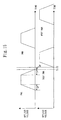
- Fig. 2 shows the operation of the first phase modulator 71, the second phase modulator 73, the first phase modulator 81, and the second phase modulator 83.
- Fig. 2 shows a voltage applied to the first optical signal, and (b) shows a voltage applied to the second optical signal.
- the operating time of the first phase modulator 71 overlaps with the operating time of the second phase modulator 73 by a period shown as OP. Namely, before a first modulation step in which the first phase modulator 71 performs the phase modulation on the first optical signal is finished, a second modulation step in which the second phase modulator 73 performs the phase modulation on the second optical signal is started. In this way, it is possible to have overlapped operating time OP between the first modulation step and the second modulation step, since the first phase modulator 71 and the second phase modulator 73 are connected in parallel.
- Fig. 3 is a flowchart showing the operation of the switching unit 55 of the control unit 51.
- the switching unit 55 obtains the phase modulation data 31 from the phase modulation data memory 53 serially at S11, and if there is no phase modulation data 31 at S12, the switching unit 55 finishes the phase modulation process.
- the switching unit 55 determines which of the first phase modulator 71 and the second phase modulator 73 is used for the phase modulation of the next optical signal. In this case, the first phase modulator 71 and the second phase modulator 73 is used alternately. And in case that the first phase modulator 71 is used at S14, the phase modulation data 31 is transmitted to the first voltage generating unit 57.
- the phase modulation data 31 is transmitted to the second voltage generating unit 59.
- the switching unit 55 switches the first optical switch 33 and the second optical switch 35 to the first phase modulator 71 or the second phase modulator 73 at S16.
- the switching unit 55 transmits an activation signal for generating the voltage based on the phase modulation data 31 to the voltage generating unit which applies the voltage for the phase modulation to the phase modulator and connected by the first optical switch 33 and the second optical switch 35.
- the first voltage generating unit 57 or the second voltage generating unit 59 outputs the voltage based on the phase modulation data 31 to the first phase modulator 71 or the second phase modulator 73.
- phase modulation at twice the speed at maximum is enabled by connecting two phase modulators in parallel and switching the operations of the two phase modulators. And further, if N phase modulators are connected in parallel and their operations are switched, the phase modulation at N-time the speed at maximum is enabled.
- Fig. 4 shows another example of the transmitting apparatus 100 (or the receiving apparatus 300).
- phase modulators of the first phase modulator 71, the second phase modulator 73, a third phase modulator 75, and a fourth phase modulator 77 are connected in parallel, and the operations are switched by the first optical switch 33 and the second optical switch 35.
- the voltage generating unit 58 always generates 0V, 4V, 8V, and 12V for the use of the phase modulation of four kinds of amount; 0, ⁇ /2, ⁇ , and 3 ⁇ /2. 0V is supplied to the first phase modulator 71, 4V is to the second phase modulator 73, 8V is to the third phase modulator 75, and 12V is to the fourth phase modulator 77.
- Fig. 5 explains the operations of the first phase modulator 71, the second phase modulator 73, the third phase modulator 75, and the fourth phase modulator 77 shown in Fig. 4.
- the first phase modulator 71 always performs the phase modulation of 0V
- the second phase modulator 73 always performs the one of 4V
- the third phase modulator 75 always performs the one of 8V
- the fourth phase modulator 77 always performs the one of 12V.
- the switching unit 55 switches the first optical switch 33 and the second optical switch 35 based on the four values (0, ⁇ /2, ⁇ , and 3 ⁇ /2) of the phase modulation data 31 stored in the phase modulation data memory 53. For example, as shown in Fig. 5, when the phase modulation data 31 is 3 ⁇ /2, the switching unit 55 switches the first optical switch 33 and the second optical switch 35 to S4. Then, the first optical signal is phase modulated by the voltage of 12V. Next, when the phase modulation data 31 is ⁇ , the switching unit 55 switches the first optical switch 33 and the second optical switch 35 to S3, and then, the second optical signal is phase modulated by 8V.
- Fig. 6 is a flowchart showing the operation of the switching unit 55 of the control unit 51 shown in Fig. 4.
- the switching unit 55 obtains the phase modulation data 31 stored in the phase modulation data memory 53 serially.
- the switching unit 55 finishes the phase modulation process if there is no phase modulation data 31.
- the switching unit 55 awaits the synchronous output signal 93 from the laser 91 at S23.
- the switching unit 55 instructs to switch the first optical switch 33 and the second optical switch 35 based on the value of the phase modulation data 31.
- each of the four phase modulators always performs one phase modulation (0, ⁇ /2, ⁇ , or 3 ⁇ /2), and the phase modulator is selected by the first optical switch 33 and the second optical switch 35. Accordingly, there is no need to consider the rise time and the fall time of the voltage, which enables a high-speed phase modulation.
- the time for switching the first optical switch 33 and the second optical switch 35 should be shorter by switching based on the cyclic frequency faster than the cyclic frequency C of the photon generated by the laser 91, which enables an extremely high-speed phase modulation.
- the first phase modulator 71, the second phase modulator 73, the third phase modulator 75, and the fourth phase modulator 77 are serially connected.
- the voltage generating unit 56 generates the voltage of the same value to the four phase modulators and supplies the voltages to the phase modulators at the same time.
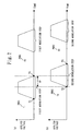
- Fig. 8 shows applied voltages to the four phase modulators.
- the rise time LP and the fall time TP are required.
- the phase modulation it is possible to apply the voltage of 8V at once to perform the phase modulation of ⁇ , and it is also possible to apply the voltage of 2V four times to perform the phase modulation of ⁇ .
- the present embodiment shortens the rise time and the fall time required for generating the voltage to perform the phase modulation by applying the voltage to perform the phase modulation dividedly. For example, as shown in Fig. 7, in order to apply the voltage to be essentially applied using four phase modulators, each of the four phase modulators applies 1/4 of the voltage. Therefore, the rise time and the fall time can be reduced to 1/4.
- the voltages of 2V are supplied to the four phase modulators at the same time. This is because it is possible to regard the time required for carrying the optical signal from the first phase modulator 71 through the fourth phase modulator 77 as almost 0, since the distance between the locations of the first phase modulator 71 and the fourth phase modulator 77 is short. If the time required for carrying the optical signal from the first phase modulator 71 through the fourth phase modulator 77 is too long to be ignored, the timings to supply the applied voltage to each phase modulator should be staggered a little.
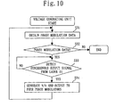
- Fig. 10 is a flowchart showing the operation of the voltage generating unit 56 of the control unit 51.
- the voltage generating unit 56 obtains the phase modulation data 31 from the phase modulation data memory 53 at S31. Next, if there is no phase modulation data 31, the voltage generating unit 56 finishes the phase modulation process at S32. Then, the voltage generating unit 56 awaits an input of the synchronous output signal 93 at S33. Further, at S34, the voltage generating unit 56 generates 1/4 of the voltage (V/4) of the voltage V which is originally indicated by the phase modulation data 31 and outputs to the four phase modulators at the same time.
- the voltage of 8V is divided into four.
- the applied voltage is 4V
- the voltage of 1V is applied to each of the four phase modulators
- the applied voltage is 12V
- the voltage of 3V is applied to each of the four phase modulators.
- N phase modulators are connected serially, which can reduce the rise time and the fall time to 1/N, respectively.
- the first modulating step in which the optical signal is phase modulated by the first phase modulator 71, the second modulating step in which the optical signal that is phase modulated at the first modulating step is further phase modulated by the second phase modulator 73, and the third and the fourth modulating steps are provided.
- a desired phase modulation of the predetermined amount can be performed.
- multiple phase modulators are connected serially and the modulated phase is divided and applied, so that the rise time and the fall time of the voltage are reduced, which enables a high-speed operation.
- Figs. 11 through 13 show examples of connecting the transmitting apparatus 100 and the receiving apparatus 300.
- Fig. 11 shows a case in which N phase modulators are connected serially.
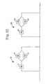
- Fig. 12 shows a case in which the phase modulators are connected in serial and partially in parallel.
- Fig. 13 shows a case in which the phase modulators are connected in parallel, and further connected in serial.
- phase modulators can be also embodied, which is not illustrated here.
- the above phase modulator can be used for the high-speed modulator in the quantum cryptography of the phase modulation system.
- the application is not limited to the quantum cryptography, but the phase modulator can be also used for the phase modulation of the optical signal.
- the above-described configuration can be used in only one of the transmitting apparatus and the receiving apparatus.
- the value of the bit rate can be increased in the quantum cryptography employing the phase modulation system. Namely, the high-speed operation can be done without the influence of the rise time and the fall time of the voltage to be applied for the phase modulation, or the influence of these time can be extremely reduced.
- phase modulation by another phase modulator can start the operation without awaiting until the voltage of the phase modulator in the process of the phase modulation is fallen to 0V, which enables the high-speed phase modulation.
- the rise time and the fall time of the voltage can be reduced to 0. Therefore, the high-speed phase modulation is enabled.
- the phase modulators are connected serially, and the voltage is divided and applied.
- the rise time and the fall time of the voltage can be reduced, which enables the high-speed phase modulation.
Landscapes
- Physics & Mathematics (AREA)
- Engineering & Computer Science (AREA)
- Electromagnetism (AREA)
- Computer Networks & Wireless Communication (AREA)
- Signal Processing (AREA)
- Optics & Photonics (AREA)
- Theoretical Computer Science (AREA)
- Computer Security & Cryptography (AREA)
- Optical Communication System (AREA)
- Optical Modulation, Optical Deflection, Nonlinear Optics, Optical Demodulation, Optical Logic Elements (AREA)
- Digital Transmission Methods That Use Modulated Carrier Waves (AREA)
- Gyroscopes (AREA)
- Amplitude Modulation (AREA)
- Transmitters (AREA)
Abstract
Description
Accordingly, the present embodiment shortens the rise time and the fall time required for generating the voltage to perform the phase modulation by applying the voltage to perform the phase modulation dividedly. For example, as shown in Fig. 7, in order to apply the voltage to be essentially applied using four phase modulators, each of the four phase modulators applies 1/4 of the voltage. Therefore, the rise time and the fall time can be reduced to 1/4.
Claims (7)
- A phase modulation apparatus comprising:N phase modulators (N: an integer equal to or greater than 2) for performing a phase modulation on an optical signal which flows through an optical path;a first optical switch and a second optical switch for selectively connecting one of the N phase modulators which are placed parallel to the optical path; anda control unit for outputting a switching signal to the first optical switch and the second optical switch and making the one of the N phase modulators connect to the optical path.
- The phase modulation apparatus of claim 1, wherein the control unit includes:a phase modulation data memory for storing phase modulation data;N voltage generating units each of which generates a voltage corresponding to each of the phase modulation to the N phase modulators; anda switching unit for serially reading the phase modulation data stored in the phase modulation data memory and serially supplying the phase modulation data read to the voltage generating unit for generating the voltage to the phase modulator to be connected to the optical path by the first optical switch and the second optical switch.
- The phase modulation apparatus of claim 1, wherein the control unit includes:a phase modulation data memory for storing phase modulation data having N values;a voltage generating unit for generating N fixed voltages corresponding to the N values of the phase modulation data, and for supplying the N fixed voltages to the N phase modulators, respectively; anda switching unit for reading the phase modulation data stored in the phase modulation data memory, and outputting the switching signal for selecting one of the N phase modulators, to which the voltage corresponding to a value of the phase modulation data read is supplied, to the first optical switch and the second optical switch.
- A phase modulation apparatus comprising:N phase modulators (N: an integer equal to or greater than 2) which are connected serially to an optical path; anda control unit for generating N voltages to the N phase modulators so that a sum of the N voltages applied to the N phase modulators becomes a voltage corresponding to a phase modulation of an optical signal, and supplying the N voltages to the N phase modulators.
- The phase modulation apparatus of claim 4, wherein the control unit includes:a phase modulation data memory for storing phase modulation data; anda voltage generating unit for generating N equal voltages (V/N) by equally dividing a voltage V, which corresponds to the phase modulation data stored in the phase modulation data memory, by N, and supplying the N equal voltages (V/N) generated to the N phase modulators, respectively.
- A phase modulation method for serially performing a phase modulation on a first optical signal and a second optical signal, the phase modulation method comprising:a first modulation step for phase modulating the first optical signal by a first phase modulator; anda second modulation step for phase modulating the second optical signal by a second phase modulator before the first modulation step terminates.
- A phase modulation method for performing a phase modulation on an optical signal by a predetermined amount comprising:a first modulation step for phase modulating the optical signal by a first phase modulator; anda second modulation step for phase modulating the optical signal, which is phase modulated by the first modulation step, by a second phase modulator, andwherein the phase modulation method performs the phase modulation on the optical signal by the predetermined amount with performing both the first modulation step and the second modulation step.
Priority Applications (1)
| Application Number | Priority Date | Filing Date | Title |
|---|---|---|---|
| EP10075149A EP2278734B1 (en) | 2000-09-11 | 2001-09-07 | Phase modulation apparatus and phase modulation method |
Applications Claiming Priority (3)
| Application Number | Priority Date | Filing Date | Title |
|---|---|---|---|
| JP2000274360A JP3841261B2 (en) | 2000-09-11 | 2000-09-11 | Phase modulation apparatus and phase modulation method |
| JP2000274360 | 2000-09-11 | ||
| PCT/JP2001/007770 WO2002023800A1 (en) | 2000-09-11 | 2001-09-07 | Phase modulator and phase modulating method |
Publications (2)
| Publication Number | Publication Date |
|---|---|
| EP1324531A1 true EP1324531A1 (en) | 2003-07-02 |
| EP1324531A4 EP1324531A4 (en) | 2008-05-21 |
Family
ID=18760129
Family Applications (2)
| Application Number | Title | Priority Date | Filing Date |
|---|---|---|---|
| EP10075149A Expired - Lifetime EP2278734B1 (en) | 2000-09-11 | 2001-09-07 | Phase modulation apparatus and phase modulation method |
| EP01963504A Withdrawn EP1324531A4 (en) | 2000-09-11 | 2001-09-07 | PHASE MODULATOR AND ITS PHASE MODULATION METHOD |
Family Applications Before (1)
| Application Number | Title | Priority Date | Filing Date |
|---|---|---|---|
| EP10075149A Expired - Lifetime EP2278734B1 (en) | 2000-09-11 | 2001-09-07 | Phase modulation apparatus and phase modulation method |
Country Status (10)
| Country | Link |
|---|---|
| US (1) | US6778314B2 (en) |
| EP (2) | EP2278734B1 (en) |
| JP (1) | JP3841261B2 (en) |
| KR (1) | KR100569769B1 (en) |
| CN (1) | CN1457571B (en) |
| AT (1) | ATE557483T1 (en) |
| AU (2) | AU2001284475B2 (en) |
| CA (1) | CA2421631C (en) |
| TW (1) | TW510102B (en) |
| WO (1) | WO2002023800A1 (en) |
Families Citing this family (17)
| Publication number | Priority date | Publication date | Assignee | Title |
|---|---|---|---|---|
| US20050191059A1 (en) * | 2004-01-12 | 2005-09-01 | Clariphy | Use of low-speed components in high-speed optical fiber transceivers |
| JPWO2005114039A1 (en) * | 2004-05-20 | 2008-03-27 | 株式会社 リーテック | Gas cylinder |
| US7369624B2 (en) * | 2004-06-01 | 2008-05-06 | Orbital Sciences Corp. | Carrier suppression type modulator with encoded modulating signals |
| US20050286723A1 (en) * | 2004-06-28 | 2005-12-29 | Magiq Technologies, Inc. | QKD system network |
| JP4936157B2 (en) * | 2005-02-22 | 2012-05-23 | 学校法人 学習院 | Quantum cryptographic communication method and quantum cryptographic communication device |
| FR2889320B1 (en) * | 2005-07-27 | 2007-10-26 | Smartquantum Sa | OPTICAL TRANSMISSION SYSTEM AND DEVICE FOR RECEIVING OPTICAL SIGNAL |
| KR100719121B1 (en) * | 2006-07-27 | 2007-05-18 | 삼성전자주식회사 | Phase modulator and manufacturing method thereof, duplexer having same |
| JP4947639B2 (en) * | 2007-01-19 | 2012-06-06 | 浜松ホトニクス株式会社 | Reflection type phase change device and setting method of reflection type phase modulation device |
| JP5126479B2 (en) * | 2007-04-16 | 2013-01-23 | 日本電気株式会社 | Quantum key distribution system and receiving apparatus |
| JP4934557B2 (en) * | 2007-09-27 | 2012-05-16 | 株式会社日立製作所 | 4-level phase modulator |
| JP5289453B2 (en) * | 2008-09-22 | 2013-09-11 | 三菱電機株式会社 | Phase modulation apparatus, transmission apparatus, reception apparatus, and phase modulation method |
| CN102456384A (en) * | 2010-10-29 | 2012-05-16 | 鸿富锦精密工业(深圳)有限公司 | Memory power supply control circuit |
| CN103259601A (en) * | 2013-04-23 | 2013-08-21 | 安徽问天量子科技股份有限公司 | Optical signal phase modulation device for quantum secret key communication |
| KR102263313B1 (en) * | 2015-01-30 | 2021-06-14 | 한국과학기술원 | Method and system for Quantum Key Distribution by Frequency-Domain Coding |
| KR101825301B1 (en) * | 2016-08-22 | 2018-02-02 | 한양대학교 산학협력단 | Signal transmission apparatus, signal transmission method and signal receive apparatus |
| CN110160573B (en) * | 2019-07-08 | 2022-03-25 | 山东省科学院激光研究所 | Escholtz ultrafast modulation pulse scanning laser and distributed optical fiber sensing system |
| CN110160572B (en) * | 2019-07-08 | 2022-03-25 | 山东省科学院激光研究所 | High-performance distributed optical fiber sensing system based on Ehrz ultrafast pulse scanning |
Family Cites Families (12)
| Publication number | Priority date | Publication date | Assignee | Title |
|---|---|---|---|---|
| FR2457505A1 (en) * | 1979-05-23 | 1980-12-19 | Thomson Csf | LIGHT INTENSITY MODULATOR WITH INTEGRATED OPTICAL DIGITAL CONTROL AND ANALOG DIGITAL CONVERTER COMPRISING SUCH A MODULATOR |
| JPH0246422A (en) | 1988-08-05 | 1990-02-15 | Fujitsu Ltd | Optical modulator |
| US5137359A (en) * | 1991-03-18 | 1992-08-11 | Litton Systems, Inc. | Digital phase modulator for fiber optic sagnac interferometer |
| US5307410A (en) * | 1993-05-25 | 1994-04-26 | International Business Machines Corporation | Interferometric quantum cryptographic key distribution system |
| JP3185835B2 (en) | 1993-11-04 | 2001-07-11 | 日本電信電話株式会社 | Optical signal expansion and compression device |
| US5644664A (en) | 1994-06-10 | 1997-07-01 | The United States Of America As Represented By The Secretary Of The Navy | Fiber optic digital transmission system |
| JPH0961771A (en) * | 1995-08-24 | 1997-03-07 | Toshiba Corp | Polarization scrambler |
| US5739943A (en) * | 1995-08-24 | 1998-04-14 | Kabushiki Kaisha Toshiba | Polarization control unit |
| JPH0996845A (en) * | 1995-09-29 | 1997-04-08 | Mitsubishi Electric Corp | Quantum computing device and quantum cryptographic device |
| DE19629260C1 (en) * | 1996-07-19 | 1998-02-26 | Litef Gmbh | Electro-optical phase modulator with direction-independent impulse response, arrangement of electro-optical phase modulators and use of an electro-optical phase modulator |
| DK0923828T3 (en) * | 1996-09-05 | 2004-05-24 | Swisscom Ag | Quantum cryptography device and method |
| US6522749B2 (en) * | 1999-01-21 | 2003-02-18 | Nec Laboratories America, Inc. | Quantum cryptographic communication channel based on quantum coherence |
-
2000
- 2000-09-11 JP JP2000274360A patent/JP3841261B2/en not_active Expired - Fee Related
-
2001
- 2001-09-05 TW TW090121955A patent/TW510102B/en not_active IP Right Cessation
- 2001-09-07 AU AU2001284475A patent/AU2001284475B2/en not_active Ceased
- 2001-09-07 KR KR1020037003581A patent/KR100569769B1/en not_active Expired - Fee Related
- 2001-09-07 EP EP10075149A patent/EP2278734B1/en not_active Expired - Lifetime
- 2001-09-07 US US10/380,044 patent/US6778314B2/en not_active Expired - Fee Related
- 2001-09-07 WO PCT/JP2001/007770 patent/WO2002023800A1/en not_active Ceased
- 2001-09-07 AT AT10075149T patent/ATE557483T1/en active
- 2001-09-07 AU AU8447501A patent/AU8447501A/en active Pending
- 2001-09-07 EP EP01963504A patent/EP1324531A4/en not_active Withdrawn
- 2001-09-07 CN CN018153895A patent/CN1457571B/en not_active Expired - Fee Related
- 2001-09-07 CA CA002421631A patent/CA2421631C/en not_active Expired - Fee Related
Also Published As
| Publication number | Publication date |
|---|---|
| KR100569769B1 (en) | 2006-04-11 |
| CA2421631C (en) | 2007-08-28 |
| TW510102B (en) | 2002-11-11 |
| EP2278734A1 (en) | 2011-01-26 |
| JP2002084277A (en) | 2002-03-22 |
| CA2421631A1 (en) | 2003-03-05 |
| KR20030040454A (en) | 2003-05-22 |
| WO2002023800A1 (en) | 2002-03-21 |
| US20030184840A1 (en) | 2003-10-02 |
| CN1457571A (en) | 2003-11-19 |
| ATE557483T1 (en) | 2012-05-15 |
| CN1457571B (en) | 2011-06-08 |
| US6778314B2 (en) | 2004-08-17 |
| EP1324531A4 (en) | 2008-05-21 |
| AU2001284475B2 (en) | 2004-06-24 |
| AU8447501A (en) | 2002-03-26 |
| JP3841261B2 (en) | 2006-11-01 |
| EP2278734B1 (en) | 2012-05-09 |
Similar Documents
| Publication | Publication Date | Title |
|---|---|---|
| EP2278734B1 (en) | Phase modulation apparatus and phase modulation method | |
| JP4086912B2 (en) | Control device for optical modulator | |
| US5703708A (en) | Adjustable optical delay line | |
| CN106483686B (en) | Electro-optical device with electro-optical (E/O) amplitude modulator and related methods | |
| CN103022895A (en) | Laser tube power control system | |
| US6980746B2 (en) | Electronic RZ/CSRZ signal generation for optical communication systems | |
| KR950701482A (en) | Optical Signal Clock Recovery Device and Method (CLOCK RECOVERY) | |
| JPH07147562A (en) | Optical device for timing recovery of encoded signal | |
| CN103001122B (en) | Power control system of double-closed-loop laser tube | |
| US7876852B2 (en) | Modulator device for generating an optical transfer signal modulated by binary signal | |
| US7027466B1 (en) | Multiplexer, demultiplexer and multiplex communication system | |
| CN110168966A (en) | Optic communication driving circuit and method, optic communication transmitting terminal, system, the vehicles | |
| CN202977971U (en) | Double-closed loop laser tube power control system | |
| EP1052792A2 (en) | Optical transmitter | |
| US7013091B2 (en) | Synchronization of pulse and data sources | |
| CN1813430B (en) | Optical Communication Signal Transmitter | |
| JP2008141671A (en) | Optical modulator, optical transmitter and optical transmission system | |
| CN202977970U (en) | Laser tube power control system | |
| JP2014029411A (en) | Optical output device and optical output method | |
| JP2006259741A (en) | Electrooptical switching device requiring no dc bias | |
| JP2000216480A (en) | Semiconductor laser drive circuit | |
| KR100763896B1 (en) | Laser diode driving method and apparatus for optical communication | |
| JP2002040379A (en) | Light intensity modulation device and double-phase type ln modulator | |
| CN111342954A (en) | Random pulse generating system | |
| JP2007081222A (en) | Semiconductor laser drive device |
Legal Events
| Date | Code | Title | Description |
|---|---|---|---|
| PUAI | Public reference made under article 153(3) epc to a published international application that has entered the european phase |
Free format text: ORIGINAL CODE: 0009012 |
|
| 17P | Request for examination filed |
Effective date: 20030305 |
|
| AK | Designated contracting states |
Designated state(s): AT BE CH CY DE DK ES FI FR GB GR IE IT LI LU MC NL PT SE TR |
|
| RAP1 | Party data changed (applicant data changed or rights of an application transferred) |
Owner name: MITSUBISHI DENKI KABUSHIKI KAISHA |
|
| A4 | Supplementary search report drawn up and despatched |
Effective date: 20080418 |
|
| RIC1 | Information provided on ipc code assigned before grant |
Ipc: H04L 9/08 20060101ALI20080414BHEP Ipc: G02F 1/01 20060101ALI20080414BHEP Ipc: H04B 10/155 20060101AFI20080414BHEP Ipc: H04B 10/30 20060101ALI20080414BHEP |
|
| 17Q | First examination report despatched |
Effective date: 20080707 |
|
| STAA | Information on the status of an ep patent application or granted ep patent |
Free format text: STATUS: THE APPLICATION IS DEEMED TO BE WITHDRAWN |
|
| 18D | Application deemed to be withdrawn |
Effective date: 20100421 |