EP1324526A2 - Control method and device for optical filter - Google Patents
Control method and device for optical filter Download PDFInfo
- Publication number
- EP1324526A2 EP1324526A2 EP02022951A EP02022951A EP1324526A2 EP 1324526 A2 EP1324526 A2 EP 1324526A2 EP 02022951 A EP02022951 A EP 02022951A EP 02022951 A EP02022951 A EP 02022951A EP 1324526 A2 EP1324526 A2 EP 1324526A2
- Authority
- EP
- European Patent Office
- Prior art keywords
- optical
- signal light
- wdm signal
- filter
- converting
- Prior art date
- Legal status (The legal status is an assumption and is not a legal conclusion. Google has not performed a legal analysis and makes no representation as to the accuracy of the status listed.)
- Withdrawn
Links
Images




Classifications
-
- H—ELECTRICITY
- H04—ELECTRIC COMMUNICATION TECHNIQUE
- H04B—TRANSMISSION
- H04B10/00—Transmission systems employing electromagnetic waves other than radio-waves, e.g. infrared, visible or ultraviolet light, or employing corpuscular radiation, e.g. quantum communication
- H04B10/25—Arrangements specific to fibre transmission
- H04B10/2507—Arrangements specific to fibre transmission for the reduction or elimination of distortion or dispersion
- H04B10/25073—Arrangements specific to fibre transmission for the reduction or elimination of distortion or dispersion using spectral equalisation, e.g. spectral filtering
-
- H—ELECTRICITY
- H04—ELECTRIC COMMUNICATION TECHNIQUE
- H04J—MULTIPLEX COMMUNICATION
- H04J14/00—Optical multiplex systems
- H04J14/02—Wavelength-division multiplex systems
- H04J14/0201—Add-and-drop multiplexing
- H04J14/0202—Arrangements therefor
- H04J14/0204—Broadcast and select arrangements, e.g. with an optical splitter at the input before adding or dropping
-
- H—ELECTRICITY
- H04—ELECTRIC COMMUNICATION TECHNIQUE
- H04J—MULTIPLEX COMMUNICATION
- H04J14/00—Optical multiplex systems
- H04J14/02—Wavelength-division multiplex systems
- H04J14/0201—Add-and-drop multiplexing
- H04J14/0202—Arrangements therefor
- H04J14/0205—Select and combine arrangements, e.g. with an optical combiner at the output after adding or dropping
-
- H—ELECTRICITY
- H04—ELECTRIC COMMUNICATION TECHNIQUE
- H04J—MULTIPLEX COMMUNICATION
- H04J14/00—Optical multiplex systems
- H04J14/02—Wavelength-division multiplex systems
- H04J14/0201—Add-and-drop multiplexing
- H04J14/0202—Arrangements therefor
- H04J14/021—Reconfigurable arrangements, e.g. reconfigurable optical add/drop multiplexers [ROADM] or tunable optical add/drop multiplexers [TOADM]
-
- H—ELECTRICITY
- H04—ELECTRIC COMMUNICATION TECHNIQUE
- H04J—MULTIPLEX COMMUNICATION
- H04J14/00—Optical multiplex systems
- H04J14/02—Wavelength-division multiplex systems
- H04J14/0201—Add-and-drop multiplexing
- H04J14/0202—Arrangements therefor
- H04J14/0213—Groups of channels or wave bands arrangements
Definitions
- the present invention relates to a control method and device for an optical filter, and an optical node device.
- OADM optical add/drop multiplexer
- OXC optical cross-connect
- the OADM and the OXC employ many optical functional devices such as an optical switch having a function of switching on/off light, attenuating light, or switching between one input and n outputs, and an optical wavelength filter for distributing signal light according to wavelength.
- optical functional devices such as an optical switch having a function of switching on/off light, attenuating light, or switching between one input and n outputs, and an optical wavelength filter for distributing signal light according to wavelength.
- a device for simultaneously processing optical signals having a plurality of desired wavelengths included in wavelength division multiplexed signal light is one of the important key devices for realization of the OADM. This simultaneous processing may be performed by using an AOTF (acousto-optic tunable filter), for example, thereby allowing simultaneous blocking or simultaneous extraction (dropping) of multiple wavelengths.
- AOTF acousto-optic tunable filter
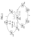
- Nodes 2(#1) to 2(#n) each provided by an OADM are connected by an optical fiber transmission line 4 to configure a ring network.
- nodes 6(#1) to 6(#n) each provided by an OADM are connected by an optical fiber transmission line 8 to configure another ring network.
- the node 2(#1) and the node 6(#1) are common.
- WDM signal light obtained by wavelength division multiplexing six channels of optical signals having different wavelengths ⁇ 1 to ⁇ 6 is transmitted from the node 2(#n) toward the node 2(#1).
- an example of the operation of the node 2(#1) is such that the node 2(#1) transmits the optical signals of the wavelengths ⁇ 1 , ⁇ 4 , and ⁇ 6 to the node 2(#2) and transmits the optical signals of the remaining wavelengths ⁇ 2 , ⁇ 3 , and ⁇ 5 to the node 6(#2).
- FIG. 2 there is shown an example of the configuration of an OADM usable as each node shown in FIG. 1.
- This OADM has an optical amplifier 10, optical coupler 12, blocking section 14, optical coupler 14, and optical amplifier 18 arranged in this order from the input port toward the output port of the OADM.
- WDM signal light input to the input port of the OADM is first amplified by the optical amplifier 10, and next branched into two WDM signal light components by the optical coupler 12.
- One of the two WDM signal light components is supplied to the blocking section 14, and the other is amplified by an optical amplifier 20 and next supplied to a drop section 22.
- the WDM signal light supplied to the drop section 22 is supplied through an optical coupler 24 to a drop filter 26, thereby separating the WDM signal light into a plurality of optical signals to be dropped.
- Each optical signal is converted into an electrical signal by a photodetector 28.
- a control circuit 30 and an RF oscillator 32 control the drop filter 26 according to the electrical signal output from the photodetector 28.
- the WDM signal light supplied to the blocking section 14 is separated into WDM signal light to be passed through the OADM and the remaining WDM signal light to be blocked, by a rejection filter 34.
- the WDM signal light to be blocked is converted into an electrical signal by a photodetector 36.
- a control circuit 38 and an RF oscillator 40 controls the rejection filter 34 according to the electrical signal output from the photodetector 36.
- the WDM signal light to be passed is supplied through the optical coupler 16 to the optical amplifier 18, and the resultant amplified WDM signal light is output from the output port of the OADM.
- An optical signal to be added to this OADM is supplied through a tunable wavelength LD 42 to an optical coupler 46 or supplied directly to the optical coupler 46.
- the tunable wavelength LD 42 performs wavelength conversion of the optical signal to be added.
- the optical signal from the optical coupler 46 is passed through the optical coupler 16, thereby being added to the WDM signal light to be passed.
- this OADM has two main functions of selectively dropping and blocking at least one optical signal of a desired single wavelength or plural wavelengths.
- the case of simultaneously dropping optical signals of plural wavelengths is a function required in the node at the overlap of two or more ring networks or networks as in the case that a plurality of wavelengths are fed from one of the networks into another network.
- the case of simultaneously blocking optical signals of plural wavelengths is applied to a wavelength required for termination of passed light in the node and a wavelength possibly colliding with a wavelength to be added.
- a device having a wavelength tuning function such as an AOTF is useful for simultaneous processing to a plurality of arbitrary wavelengths.
- the oscillation wavelength of an LD (laser diode) used as a transmitted light source has fluctuations, and the transmission center wavelength of a device itself having a wavelength characteristic of transmittance is also fluctuated by aged deterioration, environmental change, control error, etc. Therefore, it is essential to perform tracking control for detecting a wavelength shift error and performing feedback of this error, so as to obtain a stable operation.
- LD laser diode
- the tracking control is generally performed per wavelength, and only an error with respect to a wavelength to be controlled is read to control the transmission center wavelength.
- optical signals of plural wavelengths are also simultaneously output as monitor light, and it is therefore necessary to determine the correspondence between an error signal and a wavelength. Examples of the method for this determination include adding a pilot tone (or dithering) to a drive signal for a wavelength subjected to feedback, and adding dithering of frequencies different according to wavelengths.
- the wavelength subjected to feedback can be determined also in the case of plural wavelengths to be controlled, by dithering or the like.
- the number of wavelengths to be processed is increased to result in an increase in number of wavelengths output to monitor ports, the power of an optical signal having a wavelength other than the wavelengths to be controlled is increased to cause noise to a detection signal.
- the prior art has a problem that the increase in number of wavelengths causes a difficulty of control of an optical filter and a light source.
- a control method for an optical filter comprises the steps of supplying to the optical filter WDM signal light obtained by wavelength division multiplexing a plurality of optical signals having different wavelengths to obtain output WDM signal light including a part of the plurality of optical signals; converting the output WDM signal light into an electrical signal per wavelength channel of the output WDM signal light; and controlling the optical filter according to the electrical signal so that the characteristic of the optical filter becomes stable.
- a control device for an optical filter for inputting WDM signal light obtained by wavelength division multiplexing a plurality of optical signals having different wavelengths to obtain output WDM signal light including a part of the plurality of optical signals.
- This device comprises means for converting the output WDM signal light into an electrical signal per wavelength channel of the output WDM signal light; and means for controlling the optical filter according to the electrical signal so that the characteristic of the optical filter becomes stable.
- an optical node device comprising an optical filter for inputting WDM signal light obtained by wavelength division multiplexing a plurality of optical signals having different wavelengths to obtain output WDM signal light including a part of the plurality of optical signals; means for converting the output WDM signal light into an electrical signal per wavelength channel of the output WDM signal light; and means for controlling the optical filter according to the electrical signal so that the characteristic of the optical filter becomes stable.
- a method comprising the steps of supplying to an optical filter WDM signal light obtained by wavelength division multiplexing a plurality of optical signals having different wavelengths, and outputting from the optical filter output WDM signal light including a part of the plurality of optical signals; converting the output WDM signal light into an electrical signal per wavelength channel of the output WDM signal light; and controlling each optical signal of the WDM signal light according to the electrical signal so that the wavelength of each optical signal becomes stable.
- the reason for difficulty of the control in the prior art is due to multiwavelength optical powers appearing in the monitor light upon simultaneous processing.
- only a wavelength desired to be controlled is separated off in the optical domain, so as to eliminate the multiwavelength effect.
- dithering is added to each wavelength to specify a desired wavelength, and the desired wavelength is separated on an electrical stage after photodetection, thereby allowing easy separation of the desired wavelength in the optical domain.
- This device includes a rejection filter 34 as an optical filter, an optical demultiplexer 48, a plurality of photodetectors (PD) 50, and a control circuit 52 for controlling the rejection filter 34.
- WDM signal light obtained by wavelength division multiplexing a plurality of optical signals having different wavelengths ⁇ 1 to ⁇ n (n is an integer greater than 1) is supplied to the rejection filter 34.
- the rejection filter 34 effectively functions in its controlled condition to output passed light and monitor light.
- the passed light includes the optical signals of the wavelengths ⁇ 1 and ⁇ 4
- the monitor light includes the optical signals of the wavelengths ⁇ 2 , ⁇ 3 , and ⁇ n .
- the sum of the passed light and the monitor light from the rejection filter 34 is the WDM signal light supplied.
- the monitor light output from the rejection filter 34 is separated into the optical signals of the individual wavelengths by the optical demultiplexer 48, and these optical signals are converted into electrical signals by the photodetectors 50, respectively.
- the electrical signals are next supplied to the control circuit 52.
- the control circuit 52 controls the rejection filter 34 so that the wavelength characteristic of transmittance of the rejection filter 34 becomes stable.
- An AOTF may be used as the rejection filter 34, and an AWG (arrayed waveguide grating) or a dielectric multilayer filter may be used as the optical demultiplexer 48.
- AWG array waveguide grating
- dielectric multilayer filter may be used as the optical demultiplexer 48.
- a device suitable for an AOTF as an optical filter is a device having an optical waveguide and a waveguide structure for a surface acoustic wave (SAW) propagating in relation to the optical waveguide, in which both the optical waveguide and the waveguide structure are formed on a substrate.
- the optical waveguide suitable for the AOTF may be obtained by thermal diffusion of Ti on a LiNbO3 substrate having birefringence of light.
- an interdigital transducer (IDT) is also formed on the substrate, so as to propagate the surface acoustic wave in relation to the optical waveguide.
- the surface acoustic wave generated by the IDT is propagated along a predetermined path by a SAW guide, and is subsequently absorbed to be converted into heat by a saw absorber.
- WDM signal light By propagating the surface acoustic wave in relation to the optical waveguide, light having a specific wavelength determined according to the power and frequency of the surface acoustic wave and the birefringence of the optical waveguide is subjected to mode conversion from the TE mode to the TM mode or vice versa (mode converter). Accordingly, by extracting the mode-converted light by any specific means such as a polarization beam splitter, WDM signal light can be separated into selected light and unselected light. The wavelength of the selected light depends on the frequency of the surface acoustic wave, so that the wavelength of the selected light is tunable according to the frequency of the surface acoustic wave.
- FIG. 4 is a plan view of an AOTF usable as the rejection filter 34 shown in FIG. 3.
- the AOTF includes a substrate 101 formed of lithium niobate (LiNbO 3 ), an IDT 102 for generating a surface acoustic wave, polarization beam splitters 103a and 103b each for separating light into orthogonal polarization components, a SAW guide 104 for propagating the surface acoustic wave generated by the IDT 102, optical waveguides 105a and 105b for propagating the polarization components separated by the polarization beam splitter 103a, and SAW absorbers 106 and 46' each for absorbing the surface acoustic wave.
- Reference numerals 107, 108, and 109 denote input light, unselected light, and selected light, respectively.
- the input light 107 is spatially split into a TE component and a TM component by the polarization beam splitter 103a.
- the TM component propagates in the optical waveguide 105a to reach the polarization beam splitter 103b, and the TE component propagates in the optical waveguide 105b to reach the polarization beam splitter 103b.
- the polarization beam splitter 103b operates similarly to the polarization beam splitter 103a from a structural point of view, so that the TE component and the TM component are combined to be output as the unselected light 108.
- a surface acoustic wave is generated on the substrate 101.
- the sound velocity of the surface acoustic wave is lower in the region of the SAW guide 104 than in the other region around the SAW guide 104, so that the surface acoustic wave generated is confined in the region of the SAW guide 104 during propagation.
- the light propagating in the optical waveguides 105a and 105b undergoes polarization plane rotation at a specific wavelength determined by the frequency of the RF signal supplied to the IDT 102.
- the TM light propagating in the optical waveguide 105a is converted into TE light
- the TE light propagating in the optical waveguide 105b is converted into TM light before reaching the polarization beam splitter 103b.
- the TE light and the TM light having the specific wavelength thus converted are transmitted by the polarization beam splitter 103b, and therefore output as the selected light 109.
- the function of the rejection filter 34 is obtained.
- the monitor light is the selected light 109
- RF signals having frequencies (e.g., about 170 MHz) respectively uniquely corresponding to the wavelengths ⁇ 2 , ⁇ 3 , and ⁇ n are supplied from the control circuit 52 to the rejection filter 34.
- Each RF signal has a superimposed pilot tone or dithering, and synchronous detection or any other means is used to thereby stabilize the transmission center wavelength of the rejection filter 34 per channel.
- the optical demultiplexer 48 is used to separate the monitor light into a plurality of optical signals having different wavelengths, and the photodetectors 50 are used to convert the optical signals into electrical signals. Accordingly, even when the number of wavelengths to be processed is increased, there is no possibility that the powers of optical signals having wavelengths other than the wavelengths desired to be controlled may be applied to the photodetectors 50, thereby suppressing the generation of noise to the detection signals. Furthermore, it is not necessary to enlarge the dynamic range in consideration of the amplification saturation in the photodetectors 50 and their peripheral electronic circuits, so that the amplitude of the detection signals becomes relatively large to improve the S/N. Additionally, there is no possibility that the fluctuations of the other wavelengths near the dithering frequencies may degrade the detection accuracy.
- FIG. 5 is a block diagram showing a second preferred embodiment of the optical node device according to the present invention.
- a drop filter 54 as an optical filter is used in place of the rejection filter 34 shown in FIG. 3.
- WDM signal light including optical signals of wavelengths ⁇ 1 to ⁇ n is supplied to the drop filter 54, and output WDM signal light including the optical signals of the wavelengths ⁇ 2 , ⁇ 3 , and ⁇ n , for example, is output from the drop filter 54.
- the drop filter 54 has one output, and an optical coupler 56 is therefore provided to obtain the monitor light used for the control.
- the output WDM signal light from the drop filter 54 is separated into the passed light (drop light) and the monitor light by the optical coupler 56, and the passed light becomes output light from this device.
- the monitor light is separated into the optical signals of the individual wavelengths by the optical demultiplexer 48, and these optical signals are supplied to the respective photodetectors 50.
- the control circuit 52 then controls the drop filter 54 according to the electrical signals output from the photodetectors 50.
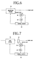
- FIG. 6 is a block diagram showing a third preferred embodiment of the optical node device according to the present invention.
- a rejection filter 34 is used as in the preferred embodiment shown in FIG. 3, and a tunable wavelength filter 58, a photodetector 60, and a control circuit 62 are used respectively in place of the optical demultiplexer 48, the photodetectors 50, and the control circuit 52 shown in FIG. 3, so as to control the rejection filter 34 so that the characteristic of the rejection filter 34 becomes stable.
- a dielectric multilayer filter or an AOTF may be used as the tunable wavelength filter 58.
- the monitor light output from the rejection filter 34 is supplied to the tunable wavelength filter 58.
- the tunable wavelength filter 58 is a bandpass filter, for example, and the center wavelength of the passband of the bandpass filter is controlled by the control circuit 62.
- An optical signal of one channel passed through the tunable wavelength filter 58 is converted into an electrical signal by the photodetector 60, and the control circuit 62 controls the rejection filter 34 according to this electrical signal.
- the center wavelength of the passband of the tunable wavelength filter 58 can be sequentially tuned to coincide with the wavelength of each optical signal of the WDM signal light by a control signal output from the control circuit 62, so that only one photodetector 60 is required for the conversion of optical signals of all the channels into electrical signals. Accordingly, by performing such time division control, the number of components can be greatly reduced over the preferred embodiment shown in FIG. 3.
- FIG. 7 is a block diagram showing a fourth preferred embodiment of the optical node device according to the present invention.
- a drop filter 54 is used as an optical filter in place of the rejection filter 34 shown in FIG. 6, and this change is accompanied by the connection of an optical coupler 56 to the output of the drop filter 54.
- the operations of the drop filter 54 and the optical coupler 56 are similar to those in the preferred embodiment shown in FIG. 5, and the operations of the tunable wavelength filter 58, the photodetector 60, and the control circuit 62 for performing the control for stabilization of the wavelength characteristic of transmittance of the drop filter 54 will be understandable substantially in accordance with the preferred embodiment shown in FIG. 6.
- FIG. 8 is a block diagram showing a fifth preferred embodiment of the optical node device according to the present invention.
- This preferred embodiment is characterized in that the rejection filter 34 and the tunable wavelength filter 58 are integrated on a common substrate 64, in contrast to the preferred embodiment shown in FIG. 6.
- the waveguide structure for the monitor light propagating from the rejection filter 34 toward the tunable wavelength filter 58 may be provided by optical fiber wiring or by an optical waveguide formed on the substrate 64.
- these components 34 and 58 can be easily formed on the substrate 64 by the same fabrication process. Accordingly, it is possible to provide an optical node device which can be easily manufactured and can be reduced in size according to this preferred embodiment.
- FIG. 9 is a block diagram showing a sixth preferred embodiment of the optical node device according to the present invention.
- This preferred embodiment is characterized in that the drop filter 54 and the tunable wavelength filter 58 are integrated on a common substrate 64, in contrast to the preferred embodiment shown in FIG. 7.
- the waveguide structure for the monitor light propagating from the drop filter 54 toward the tunable wavelength filter 58 may be provided by optical fiber wiring or by an optical waveguide formed on the substrate 64.
- these components 54 and 58 can be easily formed on the substrate 64 by the same fabrication process. Accordingly, it is possible to provide an optical node device which can be easily manufactured and can be reduced in size according to this preferred embodiment.
- FIG. 10 is a block diagram showing a seventh preferred embodiment of the optical node device according to the present invention.
- This preferred embodiment is characterized in that a rejection filter 34 and a plurality of tunable wavelength filters 58 are integrated on the substrate 64 and that a plurality of photodetectors 60 are provided so as to respectively correspond to the plural tunable wavelength filters 58, in contrast to the preferred embodiment shown in FIG. 8.
- control circuit 62 performs time division control of the rejection filter 34 for each wavelength channel in the preferred embodiment shown in FIG. 8, there is a possibility that the result of control at the subject wavelength channel may be deviated from the target in waiting for the sequence of control.
- the monitor light output from the rejection filter 34 is distributed into a plurality of powers by an optical coupler 66, and these powers are input into the tunable wavelength filters 58, respectively. Accordingly, by allocating a suitable band to each tunable wavelength filter 58, the waiting time for control in the time division control can be shortened to thereby solve the above problem.
- FIG. 11 is a block diagram showing an eighth preferred embodiment of the optical node device according to the present invention.
- This preferred embodiment is characterized in that a drop filter 54 and a plurality of tunable wavelength filters 58 are integrated on the substrate 64 and that a plurality of photodetectors 60 are provided so as to respectively correspond to the plural tunable wavelength filters 58, in contrast to the preferred embodiment shown in FIG. 9.
- control circuit 62 performs time division control of the drop filter 54 for each wavelength channel in the preferred embodiment shown in FIG. 9, there is a possibility that the result of control at the subject wavelength channel may be deviated from the target in waiting for the sequence of control.
- the monitor light output from the drop filter 54 is distributed into a plurality of powers by an optical coupler 66, and these powers are input into the tunable wavelength filters 58, respectively. Accordingly, by allocating a suitable band to each tunable wavelength filter 58, the waiting time for control in the time division control can be shortened to thereby solve the above problem.
- a light source for outputting each optical signal included in the WDM signal light may be feedback controlled according to the output from the optical filter, thereby controlling the wavelength of the subject optical signal.
Landscapes
- Engineering & Computer Science (AREA)
- Computer Networks & Wireless Communication (AREA)
- Signal Processing (AREA)
- Physics & Mathematics (AREA)
- Spectroscopy & Molecular Physics (AREA)
- Electromagnetism (AREA)
- Optical Communication System (AREA)
- Optical Modulation, Optical Deflection, Nonlinear Optics, Optical Demodulation, Optical Logic Elements (AREA)
Abstract
Description
Claims (19)
- A control method for an optical filter, comprising the steps of:supplying to said optical filter WDM signal light obtained by wavelength division multiplexing a plurality of optical signals having different wavelengths to obtain output WDM signal light including a part of said plurality of optical signals;converting said output WDM signal light into an electrical signal per wavelength channel of said output WDM signal light; andcontrolling said optical filter according to said electrical signal so that the characteristic of said optical filter becomes stable.
- A control method according to claim 1, wherein said converting step comprises the steps of supplying said output WDM signal light to an optical demultiplexer, and converting a plurality of optical signals separated by said optical demultiplexer into electrical signals by using a plurality of photodetectors, respectively.
- A control method according to claim 1, wherein said converting step comprises the steps of supplying said output WDM signal light to a tunable wavelength filter, and converting an optical signal extracted by said tunable wavelength filter into an electrical signal by using a photodetector.
- A control method according to claim 1, wherein said converting step comprises the steps of supplying said output WDM signal light to a plurality of tunable wavelength filters, and converting a plurality of optical signals extracted by said plurality of tunable wavelength filters into electrical signals by using a plurality of photodetectors, respectively.
- A control method according to claim 1,
wherein:said optical filter comprises a rejection filter;said rejection filter further outputting passed WDM signal light wherein the sum of said passed WDM signal light and said output WDM signal light is said WDM signal light. - A control method according to claim 1,
wherein:said optical filter comprises a drop filter;said control method further comprising the step of extracting a part of light passed through said drop filter to obtain said output WDM signal light. - A control device for an optical filter for inputting WDM signal light obtained by wavelength division multiplexing a plurality of optical signals. having different wavelengths to obtain output WDM signal light including a part of said plurality of optical signals, said control device comprising:means for converting said output WDM signal light into an electrical signal per wavelength channel of said output WDM signal light; andmeans for controlling said optical filter according to said electrical signal so that the characteristic of said optical filter becomes stable.
- A control device according to claim 7, wherein said converting means comprises an optical demultiplexer for inputting said output WDM signal light, and a plurality of photodetectors for converting a plurality of optical signals separated by said optical demultiplexer into electrical signals, respectively.
- A control device according to claim 7, wherein said converting means comprises a tunable wavelength filter for inputting said output WDM signal light, and a photodetector for converting an optical signal extracted by said tunable wavelength filter into an electrical signal.
- A control device according to claim 7, wherein said converting means comprises a plurality of tunable wavelength filters for inputting said output WDM signal light, and a plurality of photodetectors for converting a plurality of optical signals extracted by said plurality of tunable wavelength filters into electrical signals, respectively.
- A control device according to claim 7,
wherein:said optical filter comprises a rejection filter;said rejection filter further outputting passed WDM signal light wherein the sum of said passed WDM signal light and said output WDM signal light is said WDM signal light. - A control device according to claim 7,
wherein:said optical filter comprises a drop filter;said control device further comprising an optical coupler for extracting a part of light passed through said drop filter to obtain said output WDM signal light. - An optical node device comprising:an optical filter for inputting WDM signal light obtained by wavelength division multiplexing a plurality of optical signals having different wavelengths to obtain output WDM signal light including a part of said plurality of optical signals;means for converting said output WDM signal light into an electrical signal per wavelength channel of said output WDM signal light; andmeans for controlling said optical filter according to said electrical signal so that the characteristic of said optical filter becomes stable.
- An optical node device according to claim 13,
wherein said converting means comprises an optical demultiplexer for inputting said output WDM signal light, and a plurality of photodetectors for converting a plurality of optical signals separated by said optical demultiplexer into electrical signals, respectively. - An optical node device according to claim 13,
wherein said converting means comprises a tunable wavelength filter for inputting said output WDM signal light, and a photodetector for converting an optical signal extracted by said tunable wavelength filter into an electrical signal. - An optical node device according to claim 13,
wherein said converting means comprises a plurality of tunable wavelength filters for inputting said output WDM signal light, and a plurality of photodetectors for converting a plurality of optical signals extracted by said plurality of tunable wavelength filters into electrical signals, respectively. - An optical node device according to claim 13,
wherein:said optical filter comprises a rejection filter;said rejection filter further outputting passed WDM signal light wherein the sum of said passed WDM signal light and said output WDM signal light is said WDM signal light. - An optical node device according to claim 13,
wherein:said optical filter comprises a drop filter;said control device further comprising an optical coupler for extracting a part of light passed through said drop filter to obtain said output WDM signal light. - A method comprising the steps of:supplying to an optical filter WDM signal light obtained by wavelength division multiplexing a plurality of optical signals having different wavelengths, and outputting from said optical filter output WDM signal light including a part of said plurality of optical signals;converting said output WDM signal light into an electrical signal per wavelength channel of said output WDM signal light; andcontrolling each optical signal of said WDM signal light according to said electrical signal so that the wavelength of each optical signal becomes stable.
Applications Claiming Priority (2)
| Application Number | Priority Date | Filing Date | Title |
|---|---|---|---|
| JP2001399219 | 2001-12-28 | ||
| JP2001399219A JP3986824B2 (en) | 2001-12-28 | 2001-12-28 | Optical filter control method, control device, and optical node device |
Publications (2)
| Publication Number | Publication Date |
|---|---|
| EP1324526A2 true EP1324526A2 (en) | 2003-07-02 |
| EP1324526A3 EP1324526A3 (en) | 2005-12-14 |
Family
ID=19189445
Family Applications (1)
| Application Number | Title | Priority Date | Filing Date |
|---|---|---|---|
| EP02022951A Withdrawn EP1324526A3 (en) | 2001-12-28 | 2002-10-11 | Control method and device for optical filter |
Country Status (3)
| Country | Link |
|---|---|
| US (1) | US6895141B2 (en) |
| EP (1) | EP1324526A3 (en) |
| JP (1) | JP3986824B2 (en) |
Families Citing this family (19)
| Publication number | Priority date | Publication date | Assignee | Title |
|---|---|---|---|---|
| JP3999012B2 (en) * | 2002-03-22 | 2007-10-31 | 富士通株式会社 | Control method and control device for wavelength tunable optical filter |
| FR2841414B1 (en) * | 2002-06-20 | 2004-12-10 | Cit Alcatel | OPTICAL RING NETWORK WITH DECOUPLED READING AND WRITING FIBERS |
| JP2004235741A (en) * | 2003-01-28 | 2004-08-19 | Fujitsu Ltd | Optical transmission device and optical wavelength multiplexing network having the optical transmission device |
| US7283750B2 (en) * | 2004-07-23 | 2007-10-16 | Fujitsu Limited | System and method for setting a tunable filter in an optical network |
| JP2006235207A (en) * | 2005-02-24 | 2006-09-07 | Fujitsu Ltd | Wavelength selection control method and wavelength tunable filter device using the same |
| JP4599614B2 (en) * | 2005-08-31 | 2010-12-15 | 日本電信電話株式会社 | Optical add / drop switch |
| US7903973B1 (en) | 2005-12-23 | 2011-03-08 | Lockheed Martin Corporation | Dynamic temporal duration optical transmission privacy |
| US7792427B1 (en) | 2006-01-30 | 2010-09-07 | Lockheed Martin Corporation | Optical code division multiple access data storage and retrieval |
| US7991288B1 (en) * | 2006-02-07 | 2011-08-02 | Lockheed Martin Corporation | Optical code division multiple access data storage encryption and retrieval |
| JP4740793B2 (en) * | 2006-05-10 | 2011-08-03 | 三菱電機株式会社 | Polarization separator and optical receiver |
| WO2008024512A2 (en) * | 2006-08-24 | 2008-02-28 | Cornell Research Foundation, Inc. | Optical logic device |
| CN101247199A (en) * | 2007-02-13 | 2008-08-20 | 华为技术有限公司 | Wavelength drift detection device, wavelength locking system and method thereof |
| JP6107166B2 (en) * | 2013-01-24 | 2017-04-05 | 富士通株式会社 | Monitoring device and monitoring method for wavelength tunable optical filter |
| JP6311443B2 (en) * | 2014-05-15 | 2018-04-18 | 富士通株式会社 | Measuring apparatus, measuring method and transmission system |
| US9473263B2 (en) * | 2015-01-16 | 2016-10-18 | Huawei Technologies Co., Ltd. | Method and system for removing a pilot tone from an optical signal |
| JP6540090B2 (en) * | 2015-02-25 | 2019-07-10 | 富士通株式会社 | Receiver and transmitter |
| JP6613761B2 (en) * | 2015-09-24 | 2019-12-04 | 富士通株式会社 | Optical transmission system, control device and control method for wavelength tunable optical filter |
| JP2019061121A (en) * | 2017-09-27 | 2019-04-18 | 富士通株式会社 | Optical element and optical device |
| US20250184028A1 (en) * | 2022-03-01 | 2025-06-05 | Nippon Telegraph And Telephone Corporation | Separation system |
Family Cites Families (27)
| Publication number | Priority date | Publication date | Assignee | Title |
|---|---|---|---|---|
| US5218653A (en) | 1991-11-08 | 1993-06-08 | Bell Communications Research, Inc. | Polarization converter with apodized acoustic waveguide |
| US5276543A (en) * | 1991-11-22 | 1994-01-04 | Gte Laboratories Incorporated | Optical signal equalizer for wavelength division multiplexed optical fiber systems |
| DE4207962A1 (en) * | 1992-03-13 | 1993-09-16 | Solvay Umweltchemie Gmbh | CATALYTIC FLUID BED PROCESS FOR TREATING AQUEOUS LIQUIDS |
| JP3846918B2 (en) * | 1994-08-02 | 2006-11-15 | 富士通株式会社 | Optical transmission system, optical multiplex transmission system and related technologies |
| JP3575841B2 (en) | 1994-08-26 | 2004-10-13 | 沖電気工業株式会社 | Optical wavelength filter |
| JP3234429B2 (en) * | 1995-01-17 | 2001-12-04 | 日本電信電話株式会社 | Operation stabilizing device for mode-locked laser |
| JPH08211349A (en) | 1995-02-03 | 1996-08-20 | Tdk Corp | Wavelength variable optical filter |
| JPH08264871A (en) * | 1995-03-20 | 1996-10-11 | Fujitsu Ltd | Multi-wavelength batch optical amplifier |
| JP2937799B2 (en) | 1995-04-19 | 1999-08-23 | 日本電気株式会社 | Acousto-optic filter |
| US5504608A (en) * | 1995-05-25 | 1996-04-02 | At&T Corp. | Adjustable filter for tuning multimode optical signals |
| GB9518922D0 (en) * | 1995-09-15 | 1995-11-15 | Integrated Optical Components | Controlling optical signals |
| JPH0990303A (en) | 1995-09-25 | 1997-04-04 | Fujitsu Ltd | Wavelength filter |
| JP3739453B2 (en) * | 1995-11-29 | 2006-01-25 | 富士通株式会社 | Optical amplifier and optical communication system provided with the optical amplifier |
| US5652809A (en) | 1996-03-29 | 1997-07-29 | Aronson; Lewis B. | Offset rotated transducers for acousto-optical tunable filters |
| US6025947A (en) * | 1996-05-02 | 2000-02-15 | Fujitsu Limited | Controller which controls a variable optical attenuator to control the power level of a wavelength-multiplexed optical signal when the number of channels are varied |
| IT1282401B1 (en) | 1996-05-03 | 1998-03-20 | Pirelli Cavi S P A Ora Pirelli | SOUND-OPTICAL DEVICE IN WAVE GUIDE WITH MODAL DISPERSION COMPENSATION OF POLARIZATION |
| JPH09321701A (en) * | 1996-05-31 | 1997-12-12 | Fujitsu Ltd | Optical communication system and optical amplifier |
| CA2206945A1 (en) * | 1996-06-03 | 1997-12-03 | Tadashi Koga | Optical receiver board, optical wavelength-tuning filter module used foroptical receiver board, and actuator for optical wavelength-tuning filter module |
| JPH10163971A (en) * | 1996-11-25 | 1998-06-19 | Fujitsu Ltd | Method, apparatus and system for controlling wavelength of optical signal |
| JP3861395B2 (en) | 1997-08-11 | 2006-12-20 | 富士通株式会社 | Optical waveguide device and optical communication system using optical waveguide device |
| JPH11122192A (en) * | 1997-10-17 | 1999-04-30 | Fujitsu Ltd | Optical amplifier and optical communication system including the optical amplifier |
| JP3639109B2 (en) * | 1998-04-02 | 2005-04-20 | 富士通株式会社 | Optical transmission device, optical transmission system, and optical terminal |
| US6282340B1 (en) * | 1998-04-23 | 2001-08-28 | The Furukawa Electric Co., Ltd. | Light wavelength tuning device and light source optical demultiplexer and wavelength division multiplexed optical communication system using the tuning device |
| KR100295810B1 (en) * | 1998-06-02 | 2001-10-26 | 서평원 | Wavelength Division Multiplexing Optical Network Channel Monitoring System |
| EP1041761A3 (en) * | 1999-03-31 | 2005-07-20 | Matsushita Electric Industrial Co., Ltd. | Wavelength tunable filter apparatus |
| DE69941865D1 (en) * | 1999-08-23 | 2010-02-04 | Fujitsu Ltd | Multiplexing device for wavelength separation |
| US6636681B2 (en) * | 2001-05-07 | 2003-10-21 | Photonport Technologies, Inc. | Optical attenuator |
-
2001
- 2001-12-28 JP JP2001399219A patent/JP3986824B2/en not_active Expired - Fee Related
-
2002
- 2002-10-08 US US10/265,794 patent/US6895141B2/en not_active Expired - Fee Related
- 2002-10-11 EP EP02022951A patent/EP1324526A3/en not_active Withdrawn
Also Published As
| Publication number | Publication date |
|---|---|
| JP2003198477A (en) | 2003-07-11 |
| JP3986824B2 (en) | 2007-10-03 |
| EP1324526A3 (en) | 2005-12-14 |
| US6895141B2 (en) | 2005-05-17 |
| US20030123789A1 (en) | 2003-07-03 |
Similar Documents
| Publication | Publication Date | Title |
|---|---|---|
| US6895141B2 (en) | Control method and device for optical filter, and optical node device | |
| US7433600B2 (en) | Optical node device and system including the device | |
| US6754403B1 (en) | Acousto-optic add/drop multiplexer with retro-reflection and wavelength selective optical cross-connect | |
| US7362925B2 (en) | Control method and control apparatus of optical device | |
| US6252698B1 (en) | Method and device for wavelength conversion, and system including the device | |
| JP2003195087A (en) | Optical function device connection method and optical device | |
| JP2713324B2 (en) | Lightwave address system | |
| JP4047004B2 (en) | Method and apparatus for controlling optical wavelength tunable filter | |
| JP3293698B2 (en) | Array waveguide diffraction grating type optical multiplexer / demultiplexer with loopback optical path | |
| US7187814B2 (en) | Optical add/drop device | |
| EP1324105B1 (en) | Control method and device for optical filter | |
| JP2000324057A (en) | Monitor signal transfer device of optical transmission system | |
| JP4137440B2 (en) | Optical device connection method and optical device | |
| JP3938498B2 (en) | Optical wavelength filter | |
| JP2006235207A (en) | Wavelength selection control method and wavelength tunable filter device using the same | |
| JP2658114B2 (en) | Wavelength conversion switch | |
| JPH09127347A (en) | Wavelength selection device | |
| JP3026399B2 (en) | Polarization-independent tunable optical multiplexing / demultiplexing circuit | |
| Tian et al. | Novel fully dynamic and reconfigurable optical add/drop multiplexer based on AOTF with low crosstalk | |
| JP2006033889A (en) | Wavelength multiplexed light control device |
Legal Events
| Date | Code | Title | Description |
|---|---|---|---|
| PUAI | Public reference made under article 153(3) epc to a published international application that has entered the european phase |
Free format text: ORIGINAL CODE: 0009012 |
|
| AK | Designated contracting states |
Designated state(s): AT BE BG CH CY CZ DE DK EE ES FI FR GB GR IE IT LI LU MC NL PT SE SK TR |
|
| AX | Request for extension of the european patent |
Extension state: AL LT LV MK RO SI |
|
| PUAL | Search report despatched |
Free format text: ORIGINAL CODE: 0009013 |
|
| AK | Designated contracting states |
Kind code of ref document: A3 Designated state(s): AT BE BG CH CY CZ DE DK EE ES FI FR GB GR IE IT LI LU MC NL PT SE SK TR |
|
| AX | Request for extension of the european patent |
Extension state: AL LT LV MK RO SI |
|
| 17P | Request for examination filed |
Effective date: 20060116 |
|
| AKX | Designation fees paid |
Designated state(s): DE FR GB IT |
|
| STAA | Information on the status of an ep patent application or granted ep patent |
Free format text: STATUS: THE APPLICATION IS DEEMED TO BE WITHDRAWN |
|
| 18D | Application deemed to be withdrawn |
Effective date: 20150501 |