EP1324381A1 - Workpiece holding mechanism - Google Patents
Workpiece holding mechanism Download PDFInfo
- Publication number
- EP1324381A1 EP1324381A1 EP01984369A EP01984369A EP1324381A1 EP 1324381 A1 EP1324381 A1 EP 1324381A1 EP 01984369 A EP01984369 A EP 01984369A EP 01984369 A EP01984369 A EP 01984369A EP 1324381 A1 EP1324381 A1 EP 1324381A1
- Authority
- EP
- European Patent Office
- Prior art keywords
- electrode
- processed
- lower electrode
- detection circuit
- power source
- Prior art date
- Legal status (The legal status is an assumption and is not a legal conclusion. Google has not performed a legal analysis and makes no representation as to the accuracy of the status listed.)
- Granted
Links
Images


Classifications
-
- H—ELECTRICITY
- H10—SEMICONDUCTOR DEVICES; ELECTRIC SOLID-STATE DEVICES NOT OTHERWISE PROVIDED FOR
- H10P—GENERIC PROCESSES OR APPARATUS FOR THE MANUFACTURE OR TREATMENT OF DEVICES COVERED BY CLASS H10
- H10P72/00—Handling or holding of wafers, substrates or devices during manufacture or treatment thereof
- H10P72/50—Handling or holding of wafers, substrates or devices during manufacture or treatment thereof for positioning, orientation or alignment
-
- H—ELECTRICITY
- H10—SEMICONDUCTOR DEVICES; ELECTRIC SOLID-STATE DEVICES NOT OTHERWISE PROVIDED FOR
- H10P—GENERIC PROCESSES OR APPARATUS FOR THE MANUFACTURE OR TREATMENT OF DEVICES COVERED BY CLASS H10
- H10P72/00—Handling or holding of wafers, substrates or devices during manufacture or treatment thereof
- H10P72/70—Handling or holding of wafers, substrates or devices during manufacture or treatment thereof for supporting or gripping
- H10P72/74—Handling or holding of wafers, substrates or devices during manufacture or treatment thereof for supporting or gripping using temporarily an auxiliary support
-
- C—CHEMISTRY; METALLURGY
- C23—COATING METALLIC MATERIAL; COATING MATERIAL WITH METALLIC MATERIAL; CHEMICAL SURFACE TREATMENT; DIFFUSION TREATMENT OF METALLIC MATERIAL; COATING BY VACUUM EVAPORATION, BY SPUTTERING, BY ION IMPLANTATION OR BY CHEMICAL VAPOUR DEPOSITION, IN GENERAL; INHIBITING CORROSION OF METALLIC MATERIAL OR INCRUSTATION IN GENERAL
- C23C—COATING METALLIC MATERIAL; COATING MATERIAL WITH METALLIC MATERIAL; SURFACE TREATMENT OF METALLIC MATERIAL BY DIFFUSION INTO THE SURFACE, BY CHEMICAL CONVERSION OR SUBSTITUTION; COATING BY VACUUM EVAPORATION, BY SPUTTERING, BY ION IMPLANTATION OR BY CHEMICAL VAPOUR DEPOSITION, IN GENERAL
- C23C16/00—Chemical coating by decomposition of gaseous compounds, without leaving reaction products of surface material in the coating, i.e. chemical vapour deposition [CVD] processes
- C23C16/44—Chemical coating by decomposition of gaseous compounds, without leaving reaction products of surface material in the coating, i.e. chemical vapour deposition [CVD] processes characterised by the method of coating
- C23C16/458—Chemical coating by decomposition of gaseous compounds, without leaving reaction products of surface material in the coating, i.e. chemical vapour deposition [CVD] processes characterised by the method of coating characterised by the method used for supporting substrates in the reaction chamber
- C23C16/4581—Chemical coating by decomposition of gaseous compounds, without leaving reaction products of surface material in the coating, i.e. chemical vapour deposition [CVD] processes characterised by the method of coating characterised by the method used for supporting substrates in the reaction chamber characterised by material of construction or surface finish of the means for supporting the substrate
-
- H—ELECTRICITY
- H01—ELECTRIC ELEMENTS
- H01J—ELECTRIC DISCHARGE TUBES OR DISCHARGE LAMPS
- H01J37/00—Discharge tubes with provision for introducing objects or material to be exposed to the discharge, e.g. for the purpose of examination or processing thereof
- H01J37/02—Details
- H01J37/20—Means for supporting or positioning the object or the material; Means for adjusting diaphragms or lenses associated with the support
-
- H—ELECTRICITY
- H01—ELECTRIC ELEMENTS
- H01J—ELECTRIC DISCHARGE TUBES OR DISCHARGE LAMPS
- H01J37/00—Discharge tubes with provision for introducing objects or material to be exposed to the discharge, e.g. for the purpose of examination or processing thereof
- H01J37/32—Gas-filled discharge tubes
- H01J37/32009—Arrangements for generation of plasma specially adapted for examination or treatment of objects, e.g. plasma sources
- H01J37/32082—Radio frequency generated discharge
-
- H—ELECTRICITY
- H01—ELECTRIC ELEMENTS
- H01J—ELECTRIC DISCHARGE TUBES OR DISCHARGE LAMPS
- H01J37/00—Discharge tubes with provision for introducing objects or material to be exposed to the discharge, e.g. for the purpose of examination or processing thereof
- H01J37/32—Gas-filled discharge tubes
- H01J37/32009—Arrangements for generation of plasma specially adapted for examination or treatment of objects, e.g. plasma sources
- H01J37/32082—Radio frequency generated discharge
- H01J37/32091—Radio frequency generated discharge the radio frequency energy being capacitively coupled to the plasma
-
- H—ELECTRICITY
- H01—ELECTRIC ELEMENTS
- H01J—ELECTRIC DISCHARGE TUBES OR DISCHARGE LAMPS
- H01J37/00—Discharge tubes with provision for introducing objects or material to be exposed to the discharge, e.g. for the purpose of examination or processing thereof
- H01J37/32—Gas-filled discharge tubes
- H01J37/32009—Arrangements for generation of plasma specially adapted for examination or treatment of objects, e.g. plasma sources
- H01J37/32082—Radio frequency generated discharge
- H01J37/32174—Circuits specially adapted for controlling the RF discharge
-
- H—ELECTRICITY
- H10—SEMICONDUCTOR DEVICES; ELECTRIC SOLID-STATE DEVICES NOT OTHERWISE PROVIDED FOR
- H10P—GENERIC PROCESSES OR APPARATUS FOR THE MANUFACTURE OR TREATMENT OF DEVICES COVERED BY CLASS H10
- H10P72/00—Handling or holding of wafers, substrates or devices during manufacture or treatment thereof
- H10P72/70—Handling or holding of wafers, substrates or devices during manufacture or treatment thereof for supporting or gripping
- H10P72/72—Handling or holding of wafers, substrates or devices during manufacture or treatment thereof for supporting or gripping using electrostatic chucks
- H10P72/722—Details of electrostatic chucks
-
- Y—GENERAL TAGGING OF NEW TECHNOLOGICAL DEVELOPMENTS; GENERAL TAGGING OF CROSS-SECTIONAL TECHNOLOGIES SPANNING OVER SEVERAL SECTIONS OF THE IPC; TECHNICAL SUBJECTS COVERED BY FORMER USPC CROSS-REFERENCE ART COLLECTIONS [XRACs] AND DIGESTS
- Y10—TECHNICAL SUBJECTS COVERED BY FORMER USPC
- Y10T—TECHNICAL SUBJECTS COVERED BY FORMER US CLASSIFICATION
- Y10T279/00—Chucks or sockets
- Y10T279/23—Chucks or sockets with magnetic or electrostatic means
Definitions
- the present invention relates to a holding mechanism of an object to be processed, which is mounted in a processing chamber of a plasma processing apparatus in order to hold the object to be processed.
- an electrostatic chuck using electrostatic adsorption is used in a holding mechanism of an object to be processed such as a semiconductor wafer in a plasma processing apparatus, and the electrostatically adsorbed object to be processed is subjected to a predetermined plasma process.
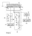
- Examples of the holding mechanism of the object to be processed include two types including a type in which a high direct-current voltage is applied to an electrode plate disposed in the electrostatic chuck shown in FIG. 5, and a type in which the electrostatic chuck is held and a high direct-current voltage is applied to an electrode for generating plasma as shown in FIG. 6.
- the former electrostatic chuck is referred to as a separated type, and the latter chuck is referred to as a coupled type.
- the separated type of holding mechanism of the object to be processed includes an electrostatic chuck 21 which electrostatically adsorbs the object to be processed (e.g., a semiconductor wafer), and a lower electrode 22 including aluminum whose surface is alumite-processed or coated with an insulating material such as ceramic.
- An upper electrode 23 is disposed above, parallel to, and opposite to the lower electrode 22 at a predetermined interval.
- the lower electrode 22 is connected to a high-frequency power source 25 via a matching circuit 24, high-frequency power is applied to the lower electrode 22 from the high-frequency power source 25, and plasma P is generated between the lower electrode 22 and upper electrode 23.
- This plasma P is collected onto a semiconductor wafer W via a focus ring 22a disposed in an outer peripheral edge of the lower electrode 22, and the semiconductor wafer is subjected to a plasma processing such as etching.
- the electrostatic chuck 21 is formed by insulating materials such as a polyimide-based resin and ceramics, and an electrode plate 21a is disposed inside the chuck.
- the electrode plate 21a is connected to a high-voltage power source 27 which applies a direct-current voltage via a filter circuit 26, the high-voltage power source 27 applies a high direct-current voltage to the electrode plate 21a, and the semiconductor wafer is electrostatically adsorbed onto a front surface of the electrostatic chuck 21.
- the filter circuit 26 includes, for example, a coil 26a, resistor 26b, and capacitor 26c, filters a high-frequency current from the high-frequency power source 25, and prevents the high-frequency current from turning onto a high-voltage power source 27 side.
- the lower electrode 22 is connected to a detection circuit 28.
- This detection circuit 28 measures a direct-current (DC) component generated in the lower electrode 22 to which the high-frequency power is applied.
- the circuit includes a coil 28a, resistor 28b, and capacitor 28c, and measures the direct-current component of a point A. At this measurement time, the circuit cuts the high-frequency current from the high-frequency power source 25, and prevents the high-frequency current from turning into the point A.
- the coupled type of holding mechanism of the object to be processed includes a constitution similar to that of the above-described separated type of holding mechanism of the object to be processed except that the lower electrode 22 also functions as the electrode plate of the electrostatic chuck 21. That is, the lower electrode 22 is connected to both the high-frequency power source 25 and high-voltage power source 27, and the high-frequency power source 25 applies the high-frequency power to the lower electrode 22 to generate the plasma P between the upper electrode 23 and lower electrode. Furthermore, the high-voltage power source 27 applies the high direct-current voltage to the lower electrode 22 to electrostatically charge the electrostatic chuck 21 and to electrostatically adsorb the semiconductor wafer.
- the detection circuit 28 also has a function as a static eliminator circuit which eliminates charges remaining in capacitor components in the lower electrode 22 and matching circuit 24.
- a property as the static eliminator circuit is sometimes used to use the detection circuit 28 as life management means of the lower electrode 22.
- the surface of the lower electrode 22 is sputtered, the alumite processing is scraped and stripped off, this stripped portion forms a closed circuit between the lower electrode 22 and upper electrode 23, and a current flows toward a detection circuit 28 side from the lower electrode 22.
- the stripped degree (wear degree) of the lower electrode 22 by the sputtering can be grasped by the magnitude of the measured value, and further the life of the lower electrode 22 can be managed.
- the detection circuit 28 measures the direct-current component in the lower electrode 22, and the direct-current component is ideally in a 0V state at times other than times when the high-frequency power is turned ON/OFF or the high voltage is turned ON/OFF. Therefore, the current flowing through the lower electrode 22 at the plasma processing time can be grasped as the current which flows through the lower electrode 22 via the stripped alumite-processed portion.
- the separated type of holding mechanism of the object to be processed shown in FIG.
- the detection circuit 28 functions as the static eliminator circuit, and a current i1 flows into the detection circuit 28 from the lower electrode 22. Therefore, a potential difference is generated between the lower electrode 22 and a focus ring 22a by the voltage drop of the lower electrode 22, and there has been a problem that this potential difference causes abnormal electric discharge between the lower electrode 22 and components such as the focus ring 22a.
- An object of the present invention is to provide a holding mechanism of an object to be processed, in which a voltage drop in an electrode can be prevented and the life of the electrode can be managed.
- a holding mechanism of an object to be processed mounted on a plasma processing apparatus which applies high-frequency power from a high-frequency power source to one of two electrodes disposed opposite to each other to generate plasma discharge, thereby subjecting the object to be processed to a plasma processing
- the mechanism comprising: an electrostatic chuck which is attached to the electrode connected to the high-frequency power source and which electrostatically adsorbs the object to be processed; a high-voltage power source which applies a direct-current voltage to the electrostatic chuck to generate an electrostatic adsorption force; a detection circuit to detect a direct-current component generated on the electrode, when the high-frequency power is applied to the electrode to subject the object to be processed to the predetermined plasma processing; and a changeover switch which can electrically disconnect the detection circuit from the electrode at processing time of the object to be processed and which can electrically connect the detection circuit to the electrode at detection time of the direct-current component or at non-processing time of the object to be processed.
- a holding mechanism of an object to be processed mounted on a plasma processing apparatus which applies high-frequency power from a high-frequency power source to one of two electrodes disposed opposite to each other to generate plasma discharge, thereby subjecting the object to be processed to a plasma processing
- the mechanism comprising: an electrostatic chuck which is attached to the electrode connected to the high-frequency power source and which electrostatically adsorbs the object to be processed; a high-voltage power source which applies a direct-current voltage to the electrode and which generates an electrostatic adsorption force in the electrostatic chuck; a detection circuit to detect a direct-current component generated on the electrode, when the high-frequency power is applied to the electrode to subject the object to be processed to the predetermined plasma processing; and a changeover switch which can electrically disconnect the detection circuit from the electrode at processing time of the object to be processed and which can electrically connect the detection circuit to the electrode at detection time of the direct-current component or at non-processing time of the object to be processed.
- FIG. 1 is a diagram showing a constitution example of a separated type, according to a first embodiment of the present invention, of a holding mechanism of an object to be processed.
- a holding mechanism 10 of the object to be processed includes: a lower electrode 2, disposed opposite to an upper electrode 7, for generating plasma; an electrostatic chuck 1 which is disposed on the lower electrode 2 to electrostatically adsorb a semiconductor wafer W; a high-voltage power source 6 which applies a direct-current voltage for generating an electrostatic adsorption force in the electrostatic chuck 1; a filter circuit 5 which prevents a high-frequency current from turning toward the high-voltage power source 6; and a detection circuit 8 which detects a direct-current component generated in the lower electrode 2 in subjecting the semiconductor wafer W to plasma process.
- the mechanism further includes: a high-frequency power source 4 which applies high-frequency power for generating the plasma; and a matching circuit 3 which obtains the matching property in the output of the high-frequency power source 4 and removes a reflected current from the lower electrode.
- the lower electrode 2 is formed of aluminum whose surface is alumite-processed or coated with an insulating material such as ceramic forming a protective film, and includes a focus ring 9 in an outer peripheral edge.
- the upper electrode 7 is disposed above the lower electrode 2, and the lower electrode 2 and upper electrode 7 are disposed parallel to each other at a predetermined interval in a processing chamber (not shown).
- the electrostatic chuck 1 is comprised of a chuck main body portion 1a formed of insulating materials such as a polyimide-based resin and ceramic, and an electrode plate 1b to which a direct-current voltage is applied from the high-voltage power source 6.
- a coil 5a and resistor 5b are connected in series between the high-voltage power source 6 and lower electrode 2
- a grounded capacitor 5c is connected to a connection point B, and the capacitor 5c filters the high-frequency current from the high-frequency power source 4 and prevents the high-frequency current from turning toward the high-voltage power source 6.
- the detection circuit 8 is comprised of a coil 8a, relay switch 8b, and resistors 8c and 8d connected in series between the lower electrode 2 and ground, and further a grounded capacitor 8e is connected between the coil 8a and relay switch 8b.
- This relay switch 8b is a constantly opened contact point, and a switch driving unit 10 switches on (conduction)/off (non-conduction) based on the instruction of a control unit (not shown) which controls the whole apparatus (not shown).
- the high-voltage power source 6 applies a high voltage to the electrode plate 1b via the filter circuit 5.
- a predetermined process gas is supplied into the processing chamber from a gas supply system (not shown) to hold a predetermined vacuum degree.
- the high-frequency power source 4 applies high-frequency power to the lower electrode 2 via the matching circuit 3 and generates plasma between the lower electrode 2 and upper electrode 7, so that the semiconductor wafer W is subjected to the predetermined plasma processing.
- the relay switch 8b is brought into an open state (non-conducting state), and the flow of direct current into the detection circuit 8 is cut off. Furthermore, at stop time of the plasma processing, or maintenance time of the plasma processing apparatus, the detection circuit 8 is brought into a closed state (conducting state), and the current is allowed to flow into the detection circuit 8.
- the relay switch 8b of the detection circuit 8 When the plasma processing is performed under a process condition easily causing the abnormal electric discharge in this manner, the relay switch 8b of the detection circuit 8 is opened. Therefore, the detection circuit 8 is electrically disconnected from the lower electrode 2 to cut off an input, voltage drop of the lower electrode 2 is prevented, and the abnormal electric discharge between the lower electrode 2 and the components such as the focus ring 9 can be prevented. Moreover, when the stripped degree of the alumite processing of the lower electrode 2 is to be detected during plasma processing not easily causing abnormal electric discharge, the relay switch 8b is closed, and the detection circuit 8 is electrically connected to the lower electrode 2.
- the stripped degree of the alumite-processed portion of the lower electrode 2 is grasped in accordance with the degree of increase of the voltage value, and further the life of the lower electrode 2 can be grasped and managed.
- the relay switch 8b is closed to connect the detection circuit 8 to the lower electrode 2, and the detection circuit 8 is allowed to function as a static eliminator circuit.
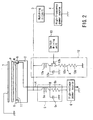
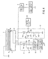
- a constitution example of a coupled type of holding mechanism of the object to be processed according to a second embodiment will next be described with reference to FIGS. 2 and 4.
- parts of the present embodiment equivalent to constituting parts shown in FIG. 1 are denoted with the same reference numerals, and description thereof is omitted.
- the above-described first embodiment includes the constitution in which the electrode plate 1b is disposed in the chuck main body 1a and the direct-current voltage is applied from the high-voltage power source 6, but the holding mechanism 20 of the object to be processed of the present embodiment includes a constitution in which the electrode plate 1b is not disposed and the lower electrode 2 is used as the electrode plate 1b.
- the holding mechanism 20 of the object to be processed shown in FIG. 2 includes: the lower electrode 2, disposed opposite to the upper electrode 7, for generating the plasma; an electrostatic chuck 11 which is disposed on the lower electrode 2 to electrostatically adsorb the semiconductor wafer W; the high-voltage power source 6 which applies the direct-current voltage to the lower electrode 2 to generate the electrostatic adsorption force in the electrostatic chuck 11; the filter circuit 5 which prevents the high-frequency current from turning toward the high-voltage power source 6; and the detection circuit 8 which detects the direct-current component generated in the lower electrode 2 in subjecting the semiconductor wafer W to the plasma processing.
- the mechanism further includes: the high-frequency power source 4 which applies the high-frequency power for generating the plasma; and the matching circuit 3 which obtains the matching property in the output of the high-frequency power source 4 and removes the reflected current from the lower electrode.
- the above-described electrostatic chuck 11 is formed of insulating materials such as polyimide-based resin or ceramic.
- the chuck is different from the electrostatic chuck 1 of the above-described first embodiment in that an electrode plate is not disposed. Therefore, the chuck is disposed on the lower electrode 2 as the electrode plate, and the direct-current voltage is applied from the high-voltage power source 6 via the lower electrode.
- a detection circuit 12 for use in the present embodiment includes substantially the same constitution as that of the detection circuit 8 of the above-described first embodiment, and is comprised of a coil 12a, relay switch 12b, and resistors 12c and 12d connected in series between the lower electrode 2 and ground, and further a grounded capacitor 12e is connected between the coil 12a and relay switch 12b.
- This relay switch 12b is a constantly opened contact point, and the switch driving unit 10 switches on (conduction)/off (non-conduction) based on the instruction of the control unit (not shown) which controls the whole apparatus (not shown).
- the constitution is equal in this manner, but there is a different respect concerning function/effect.
- the relay switch 12b is closed, the detection circuit 12 is connected to the lower electrode 2, the detection circuit 12 is used as a static eliminator circuit, and charging in the lower electrode 2 can be prevented.
- the relay switch 12b is opened, the connection of the detection circuit 12 and lower electrode 2 is canceled, the connection of the detection circuit 12 and high-voltage power source 6 is also canceled, and the function of the static eliminator circuit is stopped. This prevents the high voltage in the lower electrode 2 from dropping and can maintain the electrostatic adsorption function of the electrostatic chuck 11.
- the detection circuit 12 to function as a life manager of the lower electrode 2
- the detection circuit 12 and high-voltage power source 6 form a closed circuit
- a high output voltage from the high-voltage power source 6 is measured instead of measuring the direct-current component of the lower electrode 2, and this constitution cannot be used as a life manager of the lower electrode 2 as such.
- the present inventors have found that the current of the high-voltage power source 6 is closely associated with the bias potential Vdc of the lower electrode 2.
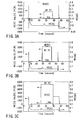
- the current HV[A] of the high-voltage power source 6 and bias potential Vdc of the lower electrode 2 change in synchronization with each other. It is further found that in synchronization with the application to the high-voltage power source 6 or high-frequency power source 4, the high-voltage current HV[A] and bias potential Vdc change.
- the lower electrode 2 and upper electrode 7 form a closed circuit via the stripped alumite-processed portion of the lower electrode 2, a current i4 flows into the high-voltage power source 6 from the lower electrode 2 as shown in FIG. 2, and the current HV[A] of the high-voltage power source 6 then changes. Therefore, in the second embodiment, the detection circuit 12 monitors the current HV[A] of the high-voltage power source 6 so that the current flowing through the stripped alumite-processed portion is indirectly grasped, and the life of the lower electrode 2 can be grasped and managed in accordance with the magnitude of the current.
- this current HV[A] can be monitored.
- an overcurrent protection circuit 13 is disposed in a power source line of the high-voltage power source 6.
- This overcurrent protection circuit 13 stops the output of the high-voltage power source 6 when a predetermined or greater overcurrent is generated by the direct-current discharge.
- a measurement circuit which measures the overcurrent is incorporated in the high-voltage power source 6.
- the circuit may also be disposed outside.
- an alarm is given based on an overcurrent detection signal in the overcurrent protection circuit 13, and the output of the high-frequency power source 4 is stopped.
- the relay switch 12b of the detection circuit 12 is brought into an open state. Since the detection circuit 12 is not connected to the lower electrode 2, the high voltage of the lower electrode 2 is prevented from dropping, and the semiconductor wafer W can be prevented from being stripped from the electrostatic chuck 11.
- the lower electrode 2 is sputtered, and a part of the alumite processing is scraped off, a closed circuit is formed between the lower electrode 2 and upper electrode 7, and the current HV[A] of the high-voltage power source 6 is monitored.
- the current HV[A] is measured at the measurement point A, the life of the lower electrode 2 is grasped in accordance with the magnitude of this current HV[A], and further the life of the lower electrode 2 can be grasped and managed.
- the relay switch 12b is closed to connect the detection circuit 12 to the lower electrode 2, and the detection circuit 12 is allowed to function as a static eliminator circuit.
- the static eliminator circuit can eliminate the static electricity.
- the overcurrent protection circuit 13 detects the overcurrent of the high-voltage power source 6 and stops the driving of the high-voltage power source 6 and high-frequency power source 4, and the alarm can be given.
- the relay switch 12b is disposed to electrically disconnect the detection circuits 8, 12 from the lower electrode 2 during a treatment in which abnormal electric discharge easily occurs and, on the other hand, to electrically connect the detection circuits 8, 12 to the lower electrode 2, when a direct-current component is detected and the semiconductor wafer W is not treated. Therefore, the following function/effect can be produced/obtained.
- the relay switch 8b of the detection circuit 8 is opened, and the detection circuit 8 is electrically disconnected from the lower electrode 2. Therefore, voltage drop of the lower electrode 2 is prevented, and abnormal electric discharge between the lower electrode 2 and components such as the focus ring 9 can be prevented.
- the relay switch 8b is closed, and the detection circuit 8 is electrically connected to the lower electrode 2. Therefore, the stripped degree of the alumite-processed portion of the lower electrode 2 is grasped in accordance with the magnitude of the voltage value at the measurement point A, and further the life of the lower electrode 2 can be grasped and managed. Moreover, life management of the lower electrode 2 under the process condition under which abnormal electric discharge easily occurs can be performed by monitoring the current HV[A] of the direct-current high-voltage power source 6.
- the relay switch 8b is closed to electrically connect the detection circuit 8 to the lower electrode 2, and the detection circuit 8 can be used as a static eliminator circuit. Therefore, charging in the lower electrode 2 at maintenance time is prevented, and an operator's short-circuit trouble can be prevented.
- the relay switch 12b of the detection circuit 12 opens, the detection circuit 12 is electrically disconnected from the lower electrode 2, and the voltage drop of the high voltage of the lower electrode 2 is prevented.
- the semiconductor wafer W can be prevented from being stripped from the electrostatic chuck 11, and further abnormal electric discharge between the lower electrode 2 and components such as the focus ring 9 can be prevented.
- the current HV[A] of the high-voltage power source 6 is monitored to grasp the life of the lower electrode 2, and further the life of the lower electrode 2 can be grasped and managed.
- the relay switch 12b is closed to electrically connect the detection circuit 12 to lower electrode 2, the detection circuit 12 can be allowed to function as a static eliminator circuit, and charging in the lower electrode 2 can be prevented.
- the overcurrent protection circuit 13 is disposed in the high-voltage power source 6 of the separated type of holding mechanism 20 of the object to be processed. Therefore, even when the direct-current discharge occurs because of the high voltage of the lower electrode 2 in the stripped alumite-processed portion of the lower electrode 2, the overcurrent protection circuit 13 detects the overcurrent of the high-voltage power source 6, the high-voltage power source 6 and high-frequency power source 4 are stopped, and the alarm can be given.
- An object of the present invention is to provide a holding mechanism of an object to be processed, which can prevent a voltage drop in an electrode and can manage the life of the electrode.
- the detection circuit for a detection circuit which has the function of detecting the stripped state of a protective film of an electrode from the direct-current component in a high-frequency power supply line and removing a residual charge, during plasma processing by a process condition under which abnormal electric discharge easily occurs, the detection circuit is electrically disconnected from a lower electrode so as to prevent abnormal electric discharge by the voltage drop of the lower electrode.
- the detection circuit is electrically connected to the lower electrode in order to detect the stripped state (life) of the protective film of the electrode from the direct-current component in the plasma discharge, or to remove charges into the lower electrode or residual charges.
- an overcurrent protection circuit stops output of the high-voltage power source and high-frequency power source.
Landscapes
- Chemical & Material Sciences (AREA)
- Analytical Chemistry (AREA)
- Engineering & Computer Science (AREA)
- Physics & Mathematics (AREA)
- Plasma & Fusion (AREA)
- Chemical Kinetics & Catalysis (AREA)
- Mechanical Engineering (AREA)
- Metallurgy (AREA)
- Organic Chemistry (AREA)
- Materials Engineering (AREA)
- General Chemical & Material Sciences (AREA)
- Container, Conveyance, Adherence, Positioning, Of Wafer (AREA)
- Drying Of Semiconductors (AREA)
Abstract
Description
Claims (6)
- A holding mechanism of an object to be processed mounted on a plasma processing apparatus which applies high-frequency power from a high-frequency power source to one of two electrodes disposed opposite to each other to generate plasma discharge, thereby subjecting the object to be processed to a plasma processing, the mechanism comprising:an electrostatic chuck which is attached to the electrode connected to the high-frequency power source and which electrostatically adsorbs the object to be processed;a high-voltage power source which applies a direct-current voltage to the electrostatic chuck to generate an electrostatic adsorption force;a detection circuit to detect a direct-current component generated on the electrode, when the high-frequency power is applied to the electrode to subject the object to be processed to the predetermined plasma processing; anda changeover switch which can electrically disconnect the detection circuit from the electrode at a processing time of the object to be processed and which can electrically connect the detection circuit to the electrode at a detection time of the direct-current component or at a non-processing time of the object to be processed.
- A holding mechanism according to claim 1, wherein the changeover switch comprises a switch driving unit to electrically disconnect the detection circuit from the electrode, when the plasma processing is performed under a process condition easily causing abnormal electric discharge, and
to electrically connect the detection circuit to the electrode and start a detection operation of the detection circuit, when a stripped degree of a protective film of the lower electrode is detected during the plasma processing under a process condition not causing the abnormal electric discharge. - A holding mechanism according to claim 1, wherein the changeover switch comprises a switch driving unit to electrically connect the detection circuit to the electrode in a state in which the plasma is not generated and to pass a charge supplied to the electrode to ground.
- A holding mechanism according to claim 1, wherein the electrostatic chuck comprises: a chuck main body portion formed of insulating materials which a polyimide-based resin or ceramic; and an electrode plate disposed in the chuck main body portion, and
the object to be processed is held by an electrostatic adsorption force generated when the high-voltage power source applies the direct-current voltage to the electrode plate. - A holding mechanism of an object to be processed mounted on a plasma processing apparatus which applies high-frequency power from a high-frequency power source to one of two electrodes disposed opposite to each other to generate plasma discharge, thereby subjecting the object to be processed to a plasma processing, the mechanism comprising:an electrostatic chuck which is attached to the electrode connected to the high-frequency power source and which electrostatically adsorbs the object to be processed;a high-voltage power source which applies a direct-current voltage to the electrode and which generates an 'electrostatic adsorption force in the electrostatic chuck;a detection circuit to detect a direct-current component generated on the electrode, when the high-frequency power is applied to the electrode to subject the object to be processed to the predetermined plasma processing; anda changeover switch which can electrically disconnect the detection circuit from the electrode at a processing time of the object to be processed and which can electrically connect the detection circuit to the electrode at a detection time of the direct-current component or at a non-processing time of the object to be processed.
- A holding mechanism of the object to be processed according to claim 5, further comprising:a measurement circuit which measures an overcurrent by direct-current discharge into the high-voltage power source from the electrode; andan overcurrent protection circuit to stop output of the high-voltage power source and high-frequency power source and to give an alarm, when a predetermined or greater overcurrent is measured.
Applications Claiming Priority (3)
| Application Number | Priority Date | Filing Date | Title |
|---|---|---|---|
| JP2000224905 | 2000-07-26 | ||
| JP2000224905A JP4590031B2 (en) | 2000-07-26 | 2000-07-26 | Placement mechanism of workpiece |
| PCT/JP2001/006420 WO2002009172A1 (en) | 2000-07-26 | 2001-07-26 | Workpiece holding mechanism |
Publications (3)
| Publication Number | Publication Date |
|---|---|
| EP1324381A1 true EP1324381A1 (en) | 2003-07-02 |
| EP1324381A4 EP1324381A4 (en) | 2009-12-23 |
| EP1324381B1 EP1324381B1 (en) | 2012-09-26 |
Family
ID=18718767
Family Applications (1)
| Application Number | Title | Priority Date | Filing Date |
|---|---|---|---|
| EP01984369A Expired - Lifetime EP1324381B1 (en) | 2000-07-26 | 2001-07-26 | Workpiece holding mechanism |
Country Status (6)
| Country | Link |
|---|---|
| US (2) | US6878233B2 (en) |
| EP (1) | EP1324381B1 (en) |
| JP (1) | JP4590031B2 (en) |
| KR (1) | KR100892790B1 (en) |
| TW (1) | TW495825B (en) |
| WO (1) | WO2002009172A1 (en) |
Families Citing this family (65)
| Publication number | Priority date | Publication date | Assignee | Title |
|---|---|---|---|---|
| JP2001316818A (en) * | 2000-02-29 | 2001-11-16 | Canon Inc | Film forming method and apparatus, silicon-based film, electromotive element, and solar cell, sensor, and image sensor using the same |
| JP4590031B2 (en) | 2000-07-26 | 2010-12-01 | 東京エレクトロン株式会社 | Placement mechanism of workpiece |
| JP4048412B2 (en) * | 2002-01-23 | 2008-02-20 | 東京エレクトロン株式会社 | Static elimination mechanism and inspection device for mounting table |
| JP4115155B2 (en) | 2002-04-11 | 2008-07-09 | 東京エレクトロン株式会社 | Method for suppressing charging of parts in vacuum processing chamber of plasma processing apparatus |
| US7541283B2 (en) * | 2002-08-30 | 2009-06-02 | Tokyo Electron Limited | Plasma processing method and plasma processing apparatus |
| KR20070072571A (en) * | 2004-11-04 | 2007-07-04 | 가부시키가이샤 알박 | Electrostatic chuck device |
| US20060275931A1 (en) * | 2005-05-20 | 2006-12-07 | Asm Japan K.K. | Technology of detecting abnormal operation of plasma process |
| JP4865352B2 (en) * | 2006-02-17 | 2012-02-01 | 三菱重工業株式会社 | Plasma processing apparatus and plasma processing method |
| JP4674177B2 (en) * | 2006-03-15 | 2011-04-20 | 株式会社日立ハイテクノロジーズ | Plasma processing equipment |
| JP5107597B2 (en) * | 2006-03-29 | 2012-12-26 | 東京エレクトロン株式会社 | Plasma processing equipment |
| US7993487B2 (en) | 2006-03-29 | 2011-08-09 | Tokyo Electron Limited | Plasma processing apparatus and method of measuring amount of radio-frequency current in plasma |
| US7655110B2 (en) | 2006-03-29 | 2010-02-02 | Tokyo Electron Limited | Plasma processing apparatus |
| JP4928817B2 (en) * | 2006-04-07 | 2012-05-09 | 株式会社日立ハイテクノロジーズ | Plasma processing equipment |
| KR100804787B1 (en) * | 2006-06-05 | 2008-02-20 | 주식회사 뉴파워 프라즈마 | Plasma processing apparatus having an active bias control circuit and its control method |
| KR100788956B1 (en) * | 2006-06-09 | 2007-12-27 | 에이피티씨 주식회사 | Plasma Process Equipment Including Electrostatic Chuck |
| DE202006020568U1 (en) * | 2006-06-30 | 2008-12-24 | Hüttinger Elektronik Gmbh + Co. Kg | Plasma process system with an electrostatic sample holding device |
| KR101394337B1 (en) * | 2006-08-30 | 2014-05-13 | 엘아이지에이디피 주식회사 | Electrostratic Chuck |
| US8343305B2 (en) * | 2007-09-04 | 2013-01-01 | Lam Research Corporation | Method and apparatus for diagnosing status of parts in real time in plasma processing equipment |
| US7884925B2 (en) * | 2008-05-23 | 2011-02-08 | Lam Research Corporation | Electrical and optical system and methods for monitoring erosion of electrostatic chuck edge bead materials |
| JP5635001B2 (en) * | 2008-09-26 | 2014-12-03 | ラム リサーチ コーポレーションLam Research Corporation | Thermal contact between electrostatic chuck and hot edge ring adjustable by clocking the coupling ring |
| JP5203986B2 (en) * | 2009-01-19 | 2013-06-05 | 東京エレクトロン株式会社 | Focus ring heating method, plasma etching method, plasma etching apparatus and computer storage medium |
| EP2390906A1 (en) * | 2010-05-26 | 2011-11-30 | Applied Materials, Inc. | Apparatus and method for electrostatic discharge (ESD) reduction |
| US10039178B2 (en) | 2010-07-16 | 2018-07-31 | Hypertherm, Inc. | Failure event detection in a plasma arc torch |
| US9761883B2 (en) | 2011-11-03 | 2017-09-12 | Johnson Controls Technology Company | Battery grid with varied corrosion resistance |
| CN103811261B (en) * | 2012-11-13 | 2016-08-24 | 中微半导体设备(上海)有限公司 | Reduce the structure of wafer leakage current and the plasma processing chamber of this structure is set |
| KR102498784B1 (en) * | 2014-12-11 | 2023-02-09 | 어플라이드 머티어리얼스, 인코포레이티드 | Electrostatic chuck for high temperature rf applications |
| JP6496579B2 (en) * | 2015-03-17 | 2019-04-03 | 東京エレクトロン株式会社 | Substrate processing method and substrate processing apparatus |
| US9754769B2 (en) * | 2015-09-15 | 2017-09-05 | Lam Research Corporation | Metrology methods to detect plasma in wafer cavity and use of the metrology for station-to-station and tool-to-tool matching |
| US10435789B2 (en) * | 2016-12-06 | 2019-10-08 | Asm Ip Holding B.V. | Substrate treatment apparatus |
| US10714372B2 (en) | 2017-09-20 | 2020-07-14 | Applied Materials, Inc. | System for coupling a voltage to portions of a substrate |
| US10510575B2 (en) | 2017-09-20 | 2019-12-17 | Applied Materials, Inc. | Substrate support with multiple embedded electrodes |
| US10555412B2 (en) | 2018-05-10 | 2020-02-04 | Applied Materials, Inc. | Method of controlling ion energy distribution using a pulse generator with a current-return output stage |
| JP6785377B2 (en) * | 2018-05-28 | 2020-11-18 | 株式会社日立ハイテク | Plasma processing equipment |
| US11476145B2 (en) | 2018-11-20 | 2022-10-18 | Applied Materials, Inc. | Automatic ESC bias compensation when using pulsed DC bias |
| KR20250100790A (en) | 2019-01-22 | 2025-07-03 | 어플라이드 머티어리얼스, 인코포레이티드 | Feedback loop for controlling a pulsed voltage waveform |
| US11508554B2 (en) | 2019-01-24 | 2022-11-22 | Applied Materials, Inc. | High voltage filter assembly |
| JP7386683B2 (en) * | 2019-12-02 | 2023-11-27 | 東京エレクトロン株式会社 | Plasma processing equipment and electrode consumption measuring method |
| JP7344821B2 (en) * | 2020-03-17 | 2023-09-14 | 東京エレクトロン株式会社 | plasma processing equipment |
| JP7466432B2 (en) * | 2020-03-24 | 2024-04-12 | 東京エレクトロン株式会社 | Plasma processing apparatus and method for measuring consumption amount |
| US11848176B2 (en) | 2020-07-31 | 2023-12-19 | Applied Materials, Inc. | Plasma processing using pulsed-voltage and radio-frequency power |
| US11798790B2 (en) | 2020-11-16 | 2023-10-24 | Applied Materials, Inc. | Apparatus and methods for controlling ion energy distribution |
| US11901157B2 (en) | 2020-11-16 | 2024-02-13 | Applied Materials, Inc. | Apparatus and methods for controlling ion energy distribution |
| JP7624305B2 (en) * | 2020-12-02 | 2025-01-30 | 東京エレクトロン株式会社 | Method for detecting wiring abnormalities and plasma processing apparatus |
| US11495470B1 (en) | 2021-04-16 | 2022-11-08 | Applied Materials, Inc. | Method of enhancing etching selectivity using a pulsed plasma |
| US11791138B2 (en) | 2021-05-12 | 2023-10-17 | Applied Materials, Inc. | Automatic electrostatic chuck bias compensation during plasma processing |
| US11948780B2 (en) | 2021-05-12 | 2024-04-02 | Applied Materials, Inc. | Automatic electrostatic chuck bias compensation during plasma processing |
| US11967483B2 (en) | 2021-06-02 | 2024-04-23 | Applied Materials, Inc. | Plasma excitation with ion energy control |
| US12525441B2 (en) | 2021-06-09 | 2026-01-13 | Applied Materials, Inc. | Plasma chamber and chamber component cleaning methods |
| US12394596B2 (en) | 2021-06-09 | 2025-08-19 | Applied Materials, Inc. | Plasma uniformity control in pulsed DC plasma chamber |
| US20220399186A1 (en) | 2021-06-09 | 2022-12-15 | Applied Materials, Inc. | Method and apparatus to reduce feature charging in plasma processing chamber |
| US11810760B2 (en) | 2021-06-16 | 2023-11-07 | Applied Materials, Inc. | Apparatus and method of ion current compensation |
| US11569066B2 (en) | 2021-06-23 | 2023-01-31 | Applied Materials, Inc. | Pulsed voltage source for plasma processing applications |
| US11776788B2 (en) | 2021-06-28 | 2023-10-03 | Applied Materials, Inc. | Pulsed voltage boost for substrate processing |
| KR102909729B1 (en) * | 2021-07-13 | 2026-01-07 | 세메스 주식회사 | Apparatus and method for inspecting electro static chuck |
| CN115706041B (en) * | 2021-08-11 | 2026-06-12 | 中微半导体设备(上海)股份有限公司 | A substrate position detection device, system and method thereof |
| US11476090B1 (en) | 2021-08-24 | 2022-10-18 | Applied Materials, Inc. | Voltage pulse time-domain multiplexing |
| US12106938B2 (en) | 2021-09-14 | 2024-10-01 | Applied Materials, Inc. | Distortion current mitigation in a radio frequency plasma processing chamber |
| US11694876B2 (en) | 2021-12-08 | 2023-07-04 | Applied Materials, Inc. | Apparatus and method for delivering a plurality of waveform signals during plasma processing |
| US11972924B2 (en) | 2022-06-08 | 2024-04-30 | Applied Materials, Inc. | Pulsed voltage source for plasma processing applications |
| US12315732B2 (en) | 2022-06-10 | 2025-05-27 | Applied Materials, Inc. | Method and apparatus for etching a semiconductor substrate in a plasma etch chamber |
| KR102716919B1 (en) * | 2022-06-24 | 2024-10-16 | 주식회사 아바코 | Apparatus for Supporting Substrate |
| US12586768B2 (en) | 2022-08-10 | 2026-03-24 | Applied Materials, Inc. | Pulsed voltage compensation for plasma processing applications |
| US12272524B2 (en) | 2022-09-19 | 2025-04-08 | Applied Materials, Inc. | Wideband variable impedance load for high volume manufacturing qualification and on-site diagnostics |
| US12111341B2 (en) | 2022-10-05 | 2024-10-08 | Applied Materials, Inc. | In-situ electric field detection method and apparatus |
| US12683123B2 (en) | 2023-12-11 | 2026-07-14 | Applied Materials, Inc. | Pulsed voltage waveform biasing of plasma |
Family Cites Families (17)
| Publication number | Priority date | Publication date | Assignee | Title |
|---|---|---|---|---|
| JPH06151373A (en) * | 1992-11-12 | 1994-05-31 | Canon Inc | Semiconductor device manufacturing equipment |
| KR100290748B1 (en) * | 1993-01-29 | 2001-06-01 | 히가시 데쓰로 | Plasma processing apparatus |
| US5557215A (en) * | 1993-05-12 | 1996-09-17 | Tokyo Electron Limited | Self-bias measuring method, apparatus thereof and electrostatic chucking apparatus |
| US5822171A (en) * | 1994-02-22 | 1998-10-13 | Applied Materials, Inc. | Electrostatic chuck with improved erosion resistance |
| US5459632A (en) * | 1994-03-07 | 1995-10-17 | Applied Materials, Inc. | Releasing a workpiece from an electrostatic chuck |
| US5900103A (en) * | 1994-04-20 | 1999-05-04 | Tokyo Electron Limited | Plasma treatment method and apparatus |
| TW293231B (en) * | 1994-04-27 | 1996-12-11 | Aneruba Kk | |
| TW286414B (en) * | 1995-07-10 | 1996-09-21 | Watkins Johnson Co | Electrostatic chuck assembly |
| US5882492A (en) * | 1996-06-21 | 1999-03-16 | Sierra Applied Sciences, Inc. | A.C. plasma processing system |
| US6214162B1 (en) * | 1996-09-27 | 2001-04-10 | Tokyo Electron Limited | Plasma processing apparatus |
| US5886865A (en) * | 1998-03-17 | 1999-03-23 | Applied Materials, Inc. | Method and apparatus for predicting failure of an eletrostatic chuck |
| JP2000049216A (en) * | 1998-07-28 | 2000-02-18 | Mitsubishi Electric Corp | Plasma processing apparatus and electrostatic chuck suction method used in the apparatus |
| JP4169839B2 (en) * | 1998-09-08 | 2008-10-22 | 株式会社アルバック | Vacuum processing apparatus and vacuum processing method |
| JP4590031B2 (en) * | 2000-07-26 | 2010-12-01 | 東京エレクトロン株式会社 | Placement mechanism of workpiece |
| KR100368116B1 (en) * | 2000-08-07 | 2003-01-15 | 삼성전자 주식회사 | Electro Stack Chuck power automatic discharge apparatus of semiconductor facilities |
| JP3665265B2 (en) * | 2000-12-28 | 2005-06-29 | 株式会社日立製作所 | Plasma processing equipment |
| JP3977114B2 (en) * | 2002-03-25 | 2007-09-19 | 株式会社ルネサステクノロジ | Plasma processing equipment |
-
2000
- 2000-07-26 JP JP2000224905A patent/JP4590031B2/en not_active Expired - Lifetime
-
2001
- 2001-07-25 TW TW090118182A patent/TW495825B/en not_active IP Right Cessation
- 2001-07-26 US US10/343,022 patent/US6878233B2/en not_active Expired - Lifetime
- 2001-07-26 EP EP01984369A patent/EP1324381B1/en not_active Expired - Lifetime
- 2001-07-26 WO PCT/JP2001/006420 patent/WO2002009172A1/en not_active Ceased
- 2001-07-26 KR KR1020037001137A patent/KR100892790B1/en not_active Expired - Fee Related
-
2005
- 2005-03-22 US US11/085,525 patent/US7265963B2/en not_active Expired - Lifetime
Also Published As
| Publication number | Publication date |
|---|---|
| TW495825B (en) | 2002-07-21 |
| US20050162805A1 (en) | 2005-07-28 |
| EP1324381B1 (en) | 2012-09-26 |
| WO2002009172A1 (en) | 2002-01-31 |
| JP2002043402A (en) | 2002-02-08 |
| US20030145950A1 (en) | 2003-08-07 |
| KR20030022315A (en) | 2003-03-15 |
| US7265963B2 (en) | 2007-09-04 |
| EP1324381A4 (en) | 2009-12-23 |
| US6878233B2 (en) | 2005-04-12 |
| JP4590031B2 (en) | 2010-12-01 |
| KR100892790B1 (en) | 2009-04-10 |
Similar Documents
| Publication | Publication Date | Title |
|---|---|---|
| EP1324381B1 (en) | Workpiece holding mechanism | |
| JP5837503B2 (en) | Method and apparatus for detecting plasma confinement in a plasma processing system | |
| KR100487823B1 (en) | Apparatus and method for actively controlling the dc potential of a cathode pedestal | |
| KR100204450B1 (en) | Arc diverter | |
| CN100510164C (en) | Method and apparatus for controlling a sputter deposition process | |
| EP1195793A2 (en) | Passive bipolar arc control system and method | |
| SG178285A1 (en) | Method and apparatus for measuring wafer bias potential | |
| KR20130041343A (en) | Direct current power supply device | |
| JP2005268214A (en) | Method and system for detecting electrical arc in plasma process in which electric power is supplied by ac power supply | |
| JP2506219B2 (en) | Electrostatic adsorption method | |
| JP2007073309A (en) | Plasma processing apparatus and method for suppressing abnormal discharge thereof | |
| CN102668722B (en) | Power-supply device | |
| US7514934B2 (en) | DC bias voltage measurement circuit and plasma CVD apparatus comprising the same | |
| WO2007014160A3 (en) | Method and apparatus for in-situ substrate surface arc detection | |
| JP2973758B2 (en) | Electrostatic chuck | |
| JP4226385B2 (en) | Plasma processing equipment | |
| JP2006117995A (en) | Sputtering apparatus | |
| JP3014867B2 (en) | Discharge detection device in vacuum equipment using discharge | |
| KR20210137187A (en) | Electrostatic adsorption device and static elimination method | |
| JP4141022B2 (en) | Sputtering method and sputtering apparatus | |
| JPH1088338A (en) | Arc counting device | |
| JPH07283137A (en) | High frequency sputtering equipment | |
| JPH11260804A (en) | Cleaning method of electrostatic adsorption electrode |
Legal Events
| Date | Code | Title | Description |
|---|---|---|---|
| PUAI | Public reference made under article 153(3) epc to a published international application that has entered the european phase |
Free format text: ORIGINAL CODE: 0009012 |
|
| 17P | Request for examination filed |
Effective date: 20030226 |
|
| AK | Designated contracting states |
Designated state(s): AT BE CH CY DE DK ES FI FR GB GR IE IT LI LU MC NL PT SE TR |
|
| A4 | Supplementary search report drawn up and despatched |
Effective date: 20091125 |
|
| 17Q | First examination report despatched |
Effective date: 20100618 |
|
| RIC1 | Information provided on ipc code assigned before grant |
Ipc: H01L 21/683 20060101ALI20120216BHEP Ipc: H01L 21/68 20060101AFI20120216BHEP Ipc: H01L 21/3065 20060101ALI20120216BHEP Ipc: H01J 37/32 20060101ALI20120216BHEP Ipc: H01J 37/20 20060101ALI20120216BHEP Ipc: C23C 16/458 20060101ALI20120216BHEP |
|
| GRAP | Despatch of communication of intention to grant a patent |
Free format text: ORIGINAL CODE: EPIDOSNIGR1 |
|
| GRAS | Grant fee paid |
Free format text: ORIGINAL CODE: EPIDOSNIGR3 |
|
| GRAA | (expected) grant |
Free format text: ORIGINAL CODE: 0009210 |
|
| AK | Designated contracting states |
Kind code of ref document: B1 Designated state(s): AT BE CH CY DE DK ES FI FR GB GR IE IT LI LU MC NL PT SE TR |
|
| REG | Reference to a national code |
Ref country code: GB Ref legal event code: FG4D |
|
| REG | Reference to a national code |
Ref country code: CH Ref legal event code: EP |
|
| REG | Reference to a national code |
Ref country code: AT Ref legal event code: REF Ref document number: 577372 Country of ref document: AT Kind code of ref document: T Effective date: 20121015 |
|
| REG | Reference to a national code |
Ref country code: IE Ref legal event code: FG4D |
|
| REG | Reference to a national code |
Ref country code: DE Ref legal event code: R096 Ref document number: 60147169 Country of ref document: DE Effective date: 20121122 |
|
| PG25 | Lapsed in a contracting state [announced via postgrant information from national office to epo] |
Ref country code: FI Free format text: LAPSE BECAUSE OF FAILURE TO SUBMIT A TRANSLATION OF THE DESCRIPTION OR TO PAY THE FEE WITHIN THE PRESCRIBED TIME-LIMIT Effective date: 20120926 |
|
| REG | Reference to a national code |
Ref country code: AT Ref legal event code: MK05 Ref document number: 577372 Country of ref document: AT Kind code of ref document: T Effective date: 20120926 |
|
| REG | Reference to a national code |
Ref country code: NL Ref legal event code: VDEP Effective date: 20120926 |
|
| PG25 | Lapsed in a contracting state [announced via postgrant information from national office to epo] |
Ref country code: SE Free format text: LAPSE BECAUSE OF FAILURE TO SUBMIT A TRANSLATION OF THE DESCRIPTION OR TO PAY THE FEE WITHIN THE PRESCRIBED TIME-LIMIT Effective date: 20120926 Ref country code: GR Free format text: LAPSE BECAUSE OF FAILURE TO SUBMIT A TRANSLATION OF THE DESCRIPTION OR TO PAY THE FEE WITHIN THE PRESCRIBED TIME-LIMIT Effective date: 20121227 |
|
| PG25 | Lapsed in a contracting state [announced via postgrant information from national office to epo] |
Ref country code: ES Free format text: LAPSE BECAUSE OF FAILURE TO SUBMIT A TRANSLATION OF THE DESCRIPTION OR TO PAY THE FEE WITHIN THE PRESCRIBED TIME-LIMIT Effective date: 20130106 Ref country code: BE Free format text: LAPSE BECAUSE OF FAILURE TO SUBMIT A TRANSLATION OF THE DESCRIPTION OR TO PAY THE FEE WITHIN THE PRESCRIBED TIME-LIMIT Effective date: 20120926 Ref country code: NL Free format text: LAPSE BECAUSE OF FAILURE TO SUBMIT A TRANSLATION OF THE DESCRIPTION OR TO PAY THE FEE WITHIN THE PRESCRIBED TIME-LIMIT Effective date: 20120926 |
|
| PG25 | Lapsed in a contracting state [announced via postgrant information from national office to epo] |
Ref country code: PT Free format text: LAPSE BECAUSE OF FAILURE TO SUBMIT A TRANSLATION OF THE DESCRIPTION OR TO PAY THE FEE WITHIN THE PRESCRIBED TIME-LIMIT Effective date: 20130128 Ref country code: CY Free format text: LAPSE BECAUSE OF FAILURE TO SUBMIT A TRANSLATION OF THE DESCRIPTION OR TO PAY THE FEE WITHIN THE PRESCRIBED TIME-LIMIT Effective date: 20120926 |
|
| PG25 | Lapsed in a contracting state [announced via postgrant information from national office to epo] |
Ref country code: AT Free format text: LAPSE BECAUSE OF FAILURE TO SUBMIT A TRANSLATION OF THE DESCRIPTION OR TO PAY THE FEE WITHIN THE PRESCRIBED TIME-LIMIT Effective date: 20120926 |
|
| PG25 | Lapsed in a contracting state [announced via postgrant information from national office to epo] |
Ref country code: DK Free format text: LAPSE BECAUSE OF FAILURE TO SUBMIT A TRANSLATION OF THE DESCRIPTION OR TO PAY THE FEE WITHIN THE PRESCRIBED TIME-LIMIT Effective date: 20120926 |
|
| PLBE | No opposition filed within time limit |
Free format text: ORIGINAL CODE: 0009261 |
|
| STAA | Information on the status of an ep patent application or granted ep patent |
Free format text: STATUS: NO OPPOSITION FILED WITHIN TIME LIMIT |
|
| PG25 | Lapsed in a contracting state [announced via postgrant information from national office to epo] |
Ref country code: IT Free format text: LAPSE BECAUSE OF FAILURE TO SUBMIT A TRANSLATION OF THE DESCRIPTION OR TO PAY THE FEE WITHIN THE PRESCRIBED TIME-LIMIT Effective date: 20120926 |
|
| 26N | No opposition filed |
Effective date: 20130627 |
|
| REG | Reference to a national code |
Ref country code: DE Ref legal event code: R097 Ref document number: 60147169 Country of ref document: DE Effective date: 20130627 |
|
| PG25 | Lapsed in a contracting state [announced via postgrant information from national office to epo] |
Ref country code: MC Free format text: LAPSE BECAUSE OF FAILURE TO SUBMIT A TRANSLATION OF THE DESCRIPTION OR TO PAY THE FEE WITHIN THE PRESCRIBED TIME-LIMIT Effective date: 20120926 |
|
| REG | Reference to a national code |
Ref country code: CH Ref legal event code: PL |
|
| GBPC | Gb: european patent ceased through non-payment of renewal fee |
Effective date: 20130726 |
|
| REG | Reference to a national code |
Ref country code: IE Ref legal event code: MM4A |
|
| REG | Reference to a national code |
Ref country code: FR Ref legal event code: ST Effective date: 20140331 |
|
| PG25 | Lapsed in a contracting state [announced via postgrant information from national office to epo] |
Ref country code: LI Free format text: LAPSE BECAUSE OF NON-PAYMENT OF DUE FEES Effective date: 20130731 Ref country code: CH Free format text: LAPSE BECAUSE OF NON-PAYMENT OF DUE FEES Effective date: 20130731 Ref country code: GB Free format text: LAPSE BECAUSE OF NON-PAYMENT OF DUE FEES Effective date: 20130726 |
|
| PG25 | Lapsed in a contracting state [announced via postgrant information from national office to epo] |
Ref country code: FR Free format text: LAPSE BECAUSE OF NON-PAYMENT OF DUE FEES Effective date: 20130731 |
|
| PG25 | Lapsed in a contracting state [announced via postgrant information from national office to epo] |
Ref country code: IE Free format text: LAPSE BECAUSE OF NON-PAYMENT OF DUE FEES Effective date: 20130726 |
|
| PG25 | Lapsed in a contracting state [announced via postgrant information from national office to epo] |
Ref country code: TR Free format text: LAPSE BECAUSE OF FAILURE TO SUBMIT A TRANSLATION OF THE DESCRIPTION OR TO PAY THE FEE WITHIN THE PRESCRIBED TIME-LIMIT Effective date: 20120926 |
|
| PG25 | Lapsed in a contracting state [announced via postgrant information from national office to epo] |
Ref country code: LU Free format text: LAPSE BECAUSE OF NON-PAYMENT OF DUE FEES Effective date: 20130726 |
|
| PGFP | Annual fee paid to national office [announced via postgrant information from national office to epo] |
Ref country code: DE Payment date: 20200714 Year of fee payment: 20 |
|
| REG | Reference to a national code |
Ref country code: DE Ref legal event code: R071 Ref document number: 60147169 Country of ref document: DE |