EP1323721A2 - Organic metal precursor for use in forming metal-containing patterned films - Google Patents
Organic metal precursor for use in forming metal-containing patterned films Download PDFInfo
- Publication number
- EP1323721A2 EP1323721A2 EP02257784A EP02257784A EP1323721A2 EP 1323721 A2 EP1323721 A2 EP 1323721A2 EP 02257784 A EP02257784 A EP 02257784A EP 02257784 A EP02257784 A EP 02257784A EP 1323721 A2 EP1323721 A2 EP 1323721A2
- Authority
- EP
- European Patent Office
- Prior art keywords
- metal
- organic
- film
- metal precursor
- organic metal
- Prior art date
- Legal status (The legal status is an assumption and is not a legal conclusion. Google has not performed a legal analysis and makes no representation as to the accuracy of the status listed.)
- Withdrawn
Links
Images

Classifications
-
- C—CHEMISTRY; METALLURGY
- C07—ORGANIC CHEMISTRY
- C07F—ACYCLIC, CARBOCYCLIC OR HETEROCYCLIC COMPOUNDS CONTAINING ELEMENTS OTHER THAN CARBON, HYDROGEN, HALOGEN, OXYGEN, NITROGEN, SULFUR, SELENIUM OR TELLURIUM
- C07F1/00—Compounds containing elements of Groups 1 or 11 of the Periodic Table
- C07F1/10—Silver compounds
-
- C—CHEMISTRY; METALLURGY
- C23—COATING METALLIC MATERIAL; COATING MATERIAL WITH METALLIC MATERIAL; CHEMICAL SURFACE TREATMENT; DIFFUSION TREATMENT OF METALLIC MATERIAL; COATING BY VACUUM EVAPORATION, BY SPUTTERING, BY ION IMPLANTATION OR BY CHEMICAL VAPOUR DEPOSITION, IN GENERAL; INHIBITING CORROSION OF METALLIC MATERIAL OR INCRUSTATION IN GENERAL
- C23C—COATING METALLIC MATERIAL; COATING MATERIAL WITH METALLIC MATERIAL; SURFACE TREATMENT OF METALLIC MATERIAL BY DIFFUSION INTO THE SURFACE, BY CHEMICAL CONVERSION OR SUBSTITUTION; COATING BY VACUUM EVAPORATION, BY SPUTTERING, BY ION IMPLANTATION OR BY CHEMICAL VAPOUR DEPOSITION, IN GENERAL
- C23C18/00—Chemical coating by decomposition of either liquid compounds or solutions of the coating forming compounds, without leaving reaction products of surface material in the coating; Contact plating
- C23C18/02—Chemical coating by decomposition of either liquid compounds or solutions of the coating forming compounds, without leaving reaction products of surface material in the coating; Contact plating by thermal decomposition
- C23C18/08—Chemical coating by decomposition of either liquid compounds or solutions of the coating forming compounds, without leaving reaction products of surface material in the coating; Contact plating by thermal decomposition characterised by the deposition of metallic material
-
- C—CHEMISTRY; METALLURGY
- C07—ORGANIC CHEMISTRY
- C07F—ACYCLIC, CARBOCYCLIC OR HETEROCYCLIC COMPOUNDS CONTAINING ELEMENTS OTHER THAN CARBON, HYDROGEN, HALOGEN, OXYGEN, NITROGEN, SULFUR, SELENIUM OR TELLURIUM
- C07F1/00—Compounds containing elements of Groups 1 or 11 of the Periodic Table
- C07F1/005—Compounds containing elements of Groups 1 or 11 of the Periodic Table without C-Metal linkages
-
- C—CHEMISTRY; METALLURGY
- C07—ORGANIC CHEMISTRY
- C07F—ACYCLIC, CARBOCYCLIC OR HETEROCYCLIC COMPOUNDS CONTAINING ELEMENTS OTHER THAN CARBON, HYDROGEN, HALOGEN, OXYGEN, NITROGEN, SULFUR, SELENIUM OR TELLURIUM
- C07F15/00—Compounds containing elements of Groups 8, 9, 10 or 18 of the Periodic Table
- C07F15/0006—Compounds containing elements of Groups 8, 9, 10 or 18 of the Periodic Table compounds of the platinum group
- C07F15/006—Palladium compounds
- C07F15/0066—Palladium compounds without a metal-carbon linkage
-
- C—CHEMISTRY; METALLURGY
- C07—ORGANIC CHEMISTRY
- C07F—ACYCLIC, CARBOCYCLIC OR HETEROCYCLIC COMPOUNDS CONTAINING ELEMENTS OTHER THAN CARBON, HYDROGEN, HALOGEN, OXYGEN, NITROGEN, SULFUR, SELENIUM OR TELLURIUM
- C07F15/00—Compounds containing elements of Groups 8, 9, 10 or 18 of the Periodic Table
- C07F15/0006—Compounds containing elements of Groups 8, 9, 10 or 18 of the Periodic Table compounds of the platinum group
- C07F15/0086—Platinum compounds
- C07F15/0093—Platinum compounds without a metal-carbon linkage
-
- C—CHEMISTRY; METALLURGY
- C07—ORGANIC CHEMISTRY
- C07F—ACYCLIC, CARBOCYCLIC OR HETEROCYCLIC COMPOUNDS CONTAINING ELEMENTS OTHER THAN CARBON, HYDROGEN, HALOGEN, OXYGEN, NITROGEN, SULFUR, SELENIUM OR TELLURIUM
- C07F15/00—Compounds containing elements of Groups 8, 9, 10 or 18 of the Periodic Table
- C07F15/04—Nickel compounds
- C07F15/045—Nickel compounds without a metal-carbon linkage
-
- C—CHEMISTRY; METALLURGY
- C07—ORGANIC CHEMISTRY
- C07F—ACYCLIC, CARBOCYCLIC OR HETEROCYCLIC COMPOUNDS CONTAINING ELEMENTS OTHER THAN CARBON, HYDROGEN, HALOGEN, OXYGEN, NITROGEN, SULFUR, SELENIUM OR TELLURIUM
- C07F15/00—Compounds containing elements of Groups 8, 9, 10 or 18 of the Periodic Table
- C07F15/06—Cobalt compounds
- C07F15/065—Cobalt compounds without a metal-carbon linkage
-
- C—CHEMISTRY; METALLURGY
- C07—ORGANIC CHEMISTRY
- C07F—ACYCLIC, CARBOCYCLIC OR HETEROCYCLIC COMPOUNDS CONTAINING ELEMENTS OTHER THAN CARBON, HYDROGEN, HALOGEN, OXYGEN, NITROGEN, SULFUR, SELENIUM OR TELLURIUM
- C07F3/00—Compounds containing elements of Groups 2 or 12 of the Periodic Table
- C07F3/003—Compounds containing elements of Groups 2 or 12 of the Periodic Table without C-Metal linkages
Definitions
- the present invention relates, in general, to an organic metal precursor and a method for forming a metal-containing patterned film on a substrate using the same, in detail, to an organic metal precursor that enables an electroconductive metal pattern of a micro- or nano-scale to be shaped only by the aid of light without using separate photoresists and to a method for depositing a patterned film of a metal or a metal oxide on a substrate via a photo-induced chemical reaction of the organic metal precursor.
- patterned films of metal-containing materials have been made through complicated process involving: depositing a film of an organic metal compound on a silicon or glass substrate by chemical vapor deposition or atomic layer deposition; applying a photoresist film on the organometallic film by spin-coating; and patterning and etching the photoresist film by photolithography.
- a film of a metal may be deposited on a substrate through plasma deposition, sputtering or electroplating and then coated with a photosensitive resinous film, followed by patterning with light and etching of the resinous film to afford a patterned film of the metal.
- these prior techniques generally require high temperature and high vacuum conditions and involve the laborious steps of patterning and etching the films of photosensitive resin.
- Japanese Laid-Open Publication No. 62-263973 discloses a patterning method wherein electron beam is irradiated to a thin film of an organometallic compound.
- organometallic compound-containing ink is applied to a substrate, and then resulting coating film is allowed to undergo thermal-degradation by exposing to laser beam radiation to provide a patterned film of a metal.
- the substrate should be subjected to a high temperature condition, and only metal can be deposited.
- US Patent No. 5,534,312 describes that a pattern of a metal can be made through coating a substrate with a metal complex prepared by bonding one or more photosensitive organic ligands to one or more metal atoms, and exposing the substrate to electromagnetic radiation, wherein there is no necessity for applying a photosensitive resin to the coating film of the metal complex.
- the metal complex essentially consists of at least one ligand selected from the group consisting of: acetylacetonates(both substituted and unsubstituted); dialkyldithiocarbamates; carboxylate; pyridines; amines; diamines; arsines; diarsenes; phosphines; diphosphenes; arenes; alkoxy ligands; alkyl ligands; and aryl ligands.
- the complex comprises more than one ligand
- at least one of the ligand is selected from the group consisting of: oxalato; halogens; hydrogen; hydroxy; cyano; carbonyl; nitro; nitrito; nitrate; nitrosyl; ethylenes; acetylenes; thiocyanato; isothyocyanato; aquo; azides; carbonato; amines; and, thiocarbonyl.
- the metal complex goes through a photochemical reaction resulting in dissociation of the organic ligands from the central metal atoms, to produce a new metal-containing material adherent to the substrate.
- the rate of such transformation is relatively low, and consequently many hours are required to complete the patterning process, which is the critical problem with this technique.
- the present invention relates to an organic metal precursor comprising one or more organic ligands bonded to one or more metal atoms, wherein the organic ligand is rapidly dissociated from the metal atom upon exposure to light to significantly reduce the patterning time, and to the use of the same.
- an organic metal precursor compound represented by the formula (I): M m L n L' o X p in the formula (I), M is a transition metal atom selected from the group consisting of Ag, Au, Co, Cu, Pd, Ni, Pt, Zn and Cd; L is a thioether represented by the formula (II) or (III); in the formula (II), each of R 1 and R 2 , independently, is a C 1-20 straight-chain, branched-chain or cyclic alkyl, alkenyl or alkynyl group, or an allyl group; in the formula (III), each of R 3 and R 4 , independently, is a hydrogen atom, or a C 1-15 straight-chain or branched-chain alkyl group, and y is an integer from 2 to 10; L' is a ligand selected from the group consisting of amines, thiols, selenols and phosphines;
- a method for forming a pattern of a metal or a metal oxide on a substrate comprising the steps of:
- the organic metal precursors of the present invention are represented by the formula (I): M m L n L' o X p in the formula (I), M is a transition metal atom selected from the group consisting of Ag, Au, Co, Cu, Pd, Ni, Pt, Zn and Cd; L is a thioether represented by the formula (II) or (III); in the formula (II), each of R 1 and R 2 , independently, is a C 1-20 straight-chain, branched-chain or cyclic alkyl, alkenyl or alkynyl group, or an allyl group; in the formula (III), each of R 3 and R 4 , independently, is a hydrogen atom, or a C 1-15 straight-chain or branched-chain alkyl group, and y is an integer from 2 to 10; L' is a ligand selected from the group consisting of amines, thiols, selenols and phosphines; X is an ani
- the organic ligands constituting the organic metal precursor of the present invention are so photosensitive as to be rapidly dissociated and degraded from the central metal atoms upon exposure to light, producing a metal or a metal oxide adherent to a surface of a substrate. Therefore, the use of the organic metal precursor of the present invention makes the troublesome steps of applying and etching a separate film of a photosensitive resin avoidable.
- an organic metal precursor is first dissolved in a suitable organic solvent to afford a coating solution.
- the coating solution is applied to a surface of a substrate to form a film of the organic metal precursor on the substrate.
- the substrate used in the present invention includes, without limitation, substrates made of inorganic materials such as silicon and glass, as well as substrates made of organic materials such as plastic. Substrates produced by using the organic and inorganic materials in combination can be also used.
- this coating step can be accomplished through spin coating, roll coating, micro-contact printing, or spray coating.
- the film is then exposed to a light source, preferably ultraviolet light.
- the film is developed with an organic solvent capable of dissolving the organic metal precursor, which can be the same as or different from the organic solvent used in the preparation of the coating solution.
- the organic metal precursor in unmasked areas of the film is certain to undergo a photochemical reaction, where the organic ligands, L and L' dissociate from the central metal atom, M and then degrade.
- the organic ligands, L and L' dissociate from the central metal atom, M and then degrade.
- the thioether ligand, L dissociates from the central metal atom more rapidly as compared with any other organic ligands. This was verified by means of an infrared spectrometer.
- the investigation for the degree of ligand dissociation according to the irradiation time revealed that most of the organic ligands(including L and L') dissociated from the central metal atoms in 4 minutes after the irradiation.
- the organic metal precursor in exposed areas of the film is rapidly converted into a corresponding metal, or is often converted into a corresponding metal oxide by the action of atmospheric oxygen.
- the thioether ligand makes the solubility of the organic metal precursor of the present invention so improved as to quickly dissolve in any of the conventional organic solvents.
- the dissociated organic ligands are also easily washed off with an organic solvent in the subsequent developing step together with the unexposed areas of the film as described above, to provide a patterned film of a metal or a metal oxide.
- the method for forming a metal-containing patterned film according to the present invention may further comprise oxidizing, reducing and/or annealing of the patterned film for the purpose of enhancing general film properties including conductivity and adhesiveness to a substrate.
- the annealing is preferably carried out at a relatively low temperature below 300° C, preferably below 200° C in an atmosphere of H 2 /N 2 mixed gas, N 2 gas or air, so that any adverse effect of heat on the substrate can be prevented. If necessary, the annealing may be carried out in the presence of a suitable oxidant or reductant for the purpose of further oxidizing or reducing the metal or the metal oxide in the pattered film, respectively.
- the patterning method of the present invention may be substituted for the sputtering process required in manufacturing the conventional flexible displays and flat panel displays, and may be adapted for the CMP-free damascene processing and the PR-free ITO film deposition.
- Example 5 Determination of degradation rate of bis(n-propylamine silver)diethylthioether dinitrite by UV irradiation
- the organic metal precursor obtained from the above Example 4 bis(n-propylamine silver)diethylthioether dinitrite was exposed to UV light by means of a Hg-Xe lamp with periodically measuring the degradation rate thereof, and the results are shown in Fig. 1. As can be seen from Fig. 1, the organic ligands mostly dissociated from the precursor compound at about 4 minutes after the exposure.
- Example 6 Formation of a patterned film of a metal using bis(n-propylamine silver)diethylthioether dinitrite
- the resulting solution was applied to a glass substrate by using a spin coater with maintaining the rotation frequency to 2,000rpm, to afford a 1 ⁇ m thick coating film.
- the coating film was then covered with a photomask and exposed to light ranging from 200nm to 800nm in the wavelength by means of Oriel 60200(200 watts, Oriel, USA). Following the exposure for 4 minutes, the photomask was removed. Thereafter, the coating film was washed with acetonitrile so that unexposed areas of the film were removed.
- the coating film was subjected to reduction with 0.1 mol of hydrazine for 30 seconds, to afford a patterned film of silver. In Fig. 2 are shown the photograph of the pattern. The specific resistance of the silver film was determined as 15 ⁇ cm.
Landscapes
- Chemical & Material Sciences (AREA)
- Organic Chemistry (AREA)
- Mechanical Engineering (AREA)
- Metallurgy (AREA)
- General Chemical & Material Sciences (AREA)
- Chemical Kinetics & Catalysis (AREA)
- Engineering & Computer Science (AREA)
- Materials Engineering (AREA)
- Physics & Mathematics (AREA)
- Thermal Sciences (AREA)
- Chemically Coating (AREA)
- Materials For Photolithography (AREA)
- Exposure And Positioning Against Photoresist Photosensitive Materials (AREA)
- Organic Low-Molecular-Weight Compounds And Preparation Thereof (AREA)
- Exposure Of Semiconductors, Excluding Electron Or Ion Beam Exposure (AREA)
- Laminated Bodies (AREA)
- Manufacturing Of Electric Cables (AREA)
Abstract
Description
M is a transition metal atom selected from the group consisting of Ag, Au, Co, Cu, Pd, Ni, Pt, Zn and Cd;
L is a thioether represented by the formula (II) or (III);

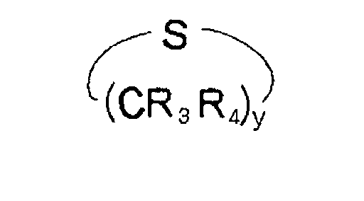
L' is a ligand selected from the group consisting of amines, thiols, selenols and phosphines;
X is an anion selected from the group consisting of halogeno, hydroxide(OH-), cyanide(CN-), nitroxyl(NO-), nitrite(NO2 -), nitrate(NO3 -), azide(N3 -), thiocyanato, isothiocyanato, tetraalkylborate, tetrahaloborate, hexafluorophosphate(PF6 -), triflate(CF3SO3-), tosylate(Ts-), sulfate(SO4 2-), and carbonate(CO3 2-);
each of m and n, independently, is an integer from 1 to 10; and
each of o and p, independently, is an integer from 0 to 10.
M is a transition metal atom selected from the group consisting of Ag, Au, Co, Cu, Pd, Ni, Pt, Zn and Cd;
L is a thioether represented by the formula (II) or (III);


L' is a ligand selected from the group consisting of amines, thiols, selenols and phosphines;
X is an anion selected from the group consisting of halogeno, hydroxide(OH-), cyanide(CN-), nitroxyl(NO-), nitrite(NO2 -), nitrate(NO3 -), azide(N3 -), thiocyanato, isothiocyanato, tetraalkylborate, tetrahaloborate, hexafluorophosphate(PF6 -), triflate(CF3SO3-), tosylate(Ts-), sulfate(SO4 2-), and carbonate(CO3 2-);
each of m and n, independently, is an integer from 1 to 10; and
each of o and p, independently, is an integer from 0 to 10.




Claims (7)
- An organic metal precursor represented by the formula (I):
M is a transition metal atom selected from Ag, Au, Co, Cu, Pd, Ni, Pt, Zn and Cd;
L is a thioether represented by the formula (II) or (III);wherein each of R1 and R2, independently, is a C1-20 straight-chain, branched-chain or cyclic alkyl, alkenyl or alkynyl group, or an allyl group;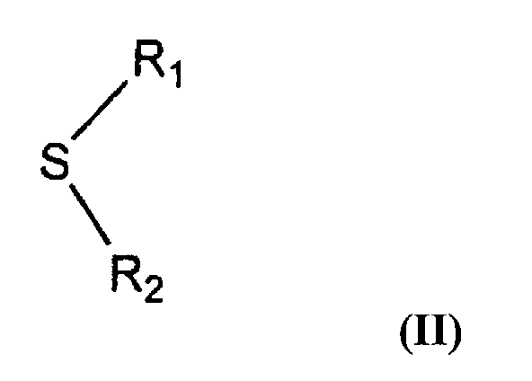 wherein, each of R3 and R4, independently, is a hydrogen atom, or a C1-15 straight-chain or branched-chain alkyl group, and y is an integer from 2 to 10;
L' is a ligand selected from amines, thiols, selenols and phosphines;
X is an anion selected halogeno, hydroxide(OH-), cyanide(CN-), nitroxyl(NO-), nitrite(NO2 -), nitrate(NO3 -), azide(N3 -), thiocyanato, isothiocyanato, tetraalkylborate, tetrahaloborate, hexafluorophosphate(PF6 -), triflate(CF3SO3-), tosylate(Ts-), sulfate(SO4 2-), and carbonate(CO3 2-);
each of m and n, independently, is an integer from 1 to 10; and
each of o and p, independently, is an integer from 0 to 10. - The organic metal precursor according to claim 1, wherein each of R1 and R2, independently, is selected from methyl, ethyl, propyl, isopropyl, isobutyl and phenyl.
- A method for forming a metal-containing patterned film on a substrate, the method comprising the steps of:(a) depositing a film of an organic metal precursor on a surface of the substrate;(b) placing a photomask of a desired pattern on the film and exposing unmasked areas of the film to a light source to cause the organic metal precursor in the unmasked area to be decomposed resulting in a patterned film of a metal or a metal oxide; and(c) washing the substrate with an organic developer capable of dissolving the organic metal precursor to remove the remaining organic metal precursor in masked areas leaving only the patterned film of a metal or a metal oxide.
- The method according to claim 3, wherein the depositing step is accomplished through spin coating, roll coating, micro-contact printing, or spray coating.
- The method according to claim 3 or 4, wherein the light source is ultraviolet light.
- The method according to any of claims 3 to 5, further comprising the step of oxidizing, reducing, or annealing the patterned film after the developing step.
- The method according to claim 6, wherein the annealing step is conducted in an atmosphere of H2/N2 mixed gas, N2 gas or air.
Applications Claiming Priority (2)
| Application Number | Priority Date | Filing Date | Title |
|---|---|---|---|
| KR2001087510 | 2001-12-28 | ||
| KR1020010087510A KR20030057133A (en) | 2001-12-28 | 2001-12-28 | Organic Metal Precursor for Forming Metal Pattern and Method for Forming Metal Pattern Using the Same |
Publications (2)
| Publication Number | Publication Date |
|---|---|
| EP1323721A2 true EP1323721A2 (en) | 2003-07-02 |
| EP1323721A3 EP1323721A3 (en) | 2003-10-08 |
Family
ID=19717856
Family Applications (1)
| Application Number | Title | Priority Date | Filing Date |
|---|---|---|---|
| EP02257784A Withdrawn EP1323721A3 (en) | 2001-12-28 | 2002-11-11 | Organic metal precursor for use in forming metal-containing patterned films |
Country Status (4)
| Country | Link |
|---|---|
| US (1) | US6965045B2 (en) |
| EP (1) | EP1323721A3 (en) |
| JP (1) | JP4172996B2 (en) |
| KR (1) | KR20030057133A (en) |
Cited By (1)
| Publication number | Priority date | Publication date | Assignee | Title |
|---|---|---|---|---|
| WO2009080642A3 (en) * | 2007-12-20 | 2009-09-17 | Technische Universität Eindhoven | Process for manufacturing conductive tracks |
Families Citing this family (16)
| Publication number | Priority date | Publication date | Assignee | Title |
|---|---|---|---|---|
| KR20030059872A (en) * | 2002-01-03 | 2003-07-12 | 삼성전자주식회사 | Process for preparing micro-pattern of metals or metal oxides |
| KR100772790B1 (en) * | 2002-04-30 | 2007-11-01 | 삼성전자주식회사 | Organometallic precursor for metal pattern formation and metal pattern formation method using the same |
| KR100545288B1 (en) * | 2003-03-28 | 2006-01-25 | 주식회사 잉크테크 | Organic silver conpound and it's preparation method, organic silver ink and it's direct wiring method |
| US20060252254A1 (en) * | 2005-05-06 | 2006-11-09 | Basol Bulent M | Filling deep and wide openings with defect-free conductor |
| US7485561B2 (en) * | 2006-03-29 | 2009-02-03 | Asm Nutool, Inc. | Filling deep features with conductors in semiconductor manufacturing |
| US7625814B2 (en) * | 2006-03-29 | 2009-12-01 | Asm Nutool, Inc. | Filling deep features with conductors in semiconductor manufacturing |
| US20090065365A1 (en) * | 2007-09-11 | 2009-03-12 | Asm Nutool, Inc. | Method and apparatus for copper electroplating |
| US7858144B2 (en) * | 2007-09-26 | 2010-12-28 | Eastman Kodak Company | Process for depositing organic materials |
| US7884016B2 (en) * | 2009-02-12 | 2011-02-08 | Asm International, N.V. | Liner materials and related processes for 3-D integration |
| CN102822385B (en) * | 2009-11-09 | 2016-09-07 | 卡内基·梅隆大学 | Metallic ink compositions, conductive patterns, methods and devices |
| TWI567205B (en) | 2011-05-04 | 2017-01-21 | 黎可德X印製金屬公司 | Method and composition for forming metal alloy from molecular ink |
| US8703386B2 (en) | 2012-02-27 | 2014-04-22 | International Business Machines Corporation | Metal peroxo compounds with organic co-ligands for electron beam, deep UV and extreme UV photoresist applications |
| US9310684B2 (en) | 2013-08-22 | 2016-04-12 | Inpria Corporation | Organometallic solution based high resolution patterning compositions |
| KR102952227B1 (en) | 2014-10-23 | 2026-04-13 | 인프리아 코포레이션 | Organometallic solution based high resolution patterning compositions and corresponding methods |
| KR102508142B1 (en) | 2015-10-13 | 2023-03-08 | 인프리아 코포레이션 | Organotin oxide hydroxide patterning compositions, precursors, and patterning |
| CN106929821B (en) * | 2017-01-17 | 2019-12-20 | 复旦大学 | Preparation method of metal nitride film with adjustable metal content and reactor |
Family Cites Families (5)
| Publication number | Priority date | Publication date | Assignee | Title |
|---|---|---|---|---|
| JPS62263973A (en) | 1986-05-08 | 1987-11-16 | Kazumichi Omura | Thin metallic film and its production |
| US4911992A (en) * | 1986-12-04 | 1990-03-27 | Dow Corning Corporation | Platinum or rhodium catalyzed multilayer ceramic coatings from hydrogen silsesquioxane resin and metal oxides |
| US5064685A (en) * | 1989-08-23 | 1991-11-12 | At&T Laboratories | Electrical conductor deposition method |
| US5534312A (en) * | 1994-11-14 | 1996-07-09 | Simon Fraser University | Method for directly depositing metal containing patterned films |
| US6099903A (en) * | 1999-05-19 | 2000-08-08 | Research Foundation Of State University Of New York | MOCVD processes using precursors based on organometalloid ligands |
-
2001
- 2001-12-28 KR KR1020010087510A patent/KR20030057133A/en not_active Withdrawn
-
2002
- 2002-10-29 US US10/282,031 patent/US6965045B2/en not_active Expired - Fee Related
- 2002-11-11 EP EP02257784A patent/EP1323721A3/en not_active Withdrawn
- 2002-12-25 JP JP2002373621A patent/JP4172996B2/en not_active Expired - Fee Related
Cited By (2)
| Publication number | Priority date | Publication date | Assignee | Title |
|---|---|---|---|---|
| WO2009080642A3 (en) * | 2007-12-20 | 2009-09-17 | Technische Universität Eindhoven | Process for manufacturing conductive tracks |
| CN101946023A (en) * | 2007-12-20 | 2011-01-12 | 艾恩德霍芬理工大学 | Make the method for conductive traces |
Also Published As
| Publication number | Publication date |
|---|---|
| JP4172996B2 (en) | 2008-10-29 |
| US6965045B2 (en) | 2005-11-15 |
| KR20030057133A (en) | 2003-07-04 |
| US20030124457A1 (en) | 2003-07-03 |
| JP2003286579A (en) | 2003-10-10 |
| EP1323721A3 (en) | 2003-10-08 |
Similar Documents
| Publication | Publication Date | Title |
|---|---|---|
| EP1323721A2 (en) | Organic metal precursor for use in forming metal-containing patterned films | |
| CN1092244C (en) | Method for direct deposition of metal-containing patterned films | |
| KR100772790B1 (en) | Organometallic precursor for metal pattern formation and metal pattern formation method using the same | |
| JPH07166372A (en) | Method for selective metallization | |
| JP2003532303A (en) | Metal and metal oxide films and methods of depositing patterned films | |
| US8715914B2 (en) | Organometallic composition for forming a metal alloy pattern and a method of forming such a pattern using the composition | |
| KR100819297B1 (en) | Manufacturing method of high reflectivity fine pattern | |
| KR100765684B1 (en) | Organometallic Precursor Mixture for Alloy Pattern Formation and Alloy Pattern Formation Method Using the Same | |
| US7374701B2 (en) | Organometallic precursor composition and method of forming metal film or pattern using the same | |
| US7033738B2 (en) | Process of forming a micro-pattern of a metal or a metal oxide | |
| US6599587B2 (en) | Organometallic precursor for forming metal pattern and method of forming metal pattern using the same | |
| US7084288B2 (en) | Organometallic precursor for forming metal film or pattern and method of forming metal film or pattern using the same | |
| KR100445314B1 (en) | Method for forming a pattern of High conductive metal by organometallic compounds | |
| EP4625043A2 (en) | Tin carboxylate precursors for metal oxide resist layers and related methods | |
| KR20040055197A (en) | Method for forming a pattern of conductive metal using organometallic compounds | |
| KR102767194B1 (en) | Tin compounds containing a tin-oxygen double bond, a photoresist composition containing the same and a method of forming a photoresist pattern using the same | |
| JP2012203236A (en) | Method for manufacturing metal thin film pattern | |
| JP2025051654A (en) | Tin compounds containing tin-oxygen double bond, and photoresist composition containing the same |
Legal Events
| Date | Code | Title | Description |
|---|---|---|---|
| PUAI | Public reference made under article 153(3) epc to a published international application that has entered the european phase |
Free format text: ORIGINAL CODE: 0009012 |
|
| AK | Designated contracting states |
Designated state(s): AT BE BG CH CY CZ DE DK EE ES FI FR GB GR IE IT LI LU MC NL PT SE SK TR |
|
| AX | Request for extension of the european patent |
Extension state: AL LT LV MK RO SI |
|
| PUAL | Search report despatched |
Free format text: ORIGINAL CODE: 0009013 |
|
| AK | Designated contracting states |
Kind code of ref document: A3 Designated state(s): AT BE BG CH CY CZ DE DK EE ES FI FR GB GR IE IT LI LU MC NL PT SE SK TR |
|
| AX | Request for extension of the european patent |
Extension state: AL LT LV MK RO SI |
|
| AKX | Designation fees paid | ||
| REG | Reference to a national code |
Ref country code: DE Ref legal event code: 8566 |
|
| STAA | Information on the status of an ep patent application or granted ep patent |
Free format text: STATUS: THE APPLICATION IS DEEMED TO BE WITHDRAWN |
|
| 18D | Application deemed to be withdrawn |
Effective date: 20040409 |